PWO460065Dual Band Signal Booster
Wilson Electronics, LLC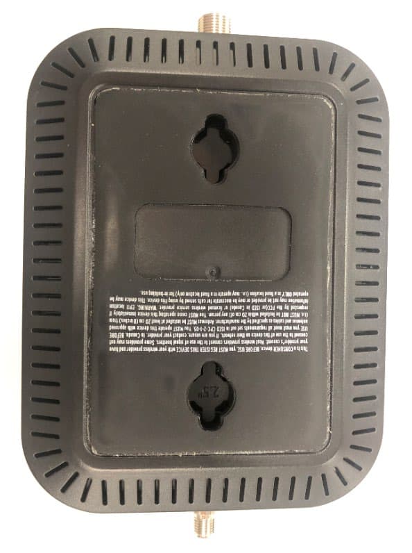
Click to zoom
Application Details
- Equipment Class
- B2W - Part 20 Wideband Consumer Booster (CMRS)
- Date of Grant
- Nov 04, 2020
- Application Purpose
- Original Equipment
- Date of Application
- Nov 04, 2020
- Equipment Note
- Dual Band Signal Booster
- Frequency Range
- 746.00000000 - 757.00000000
- Company
- Wilson Electronics, LLC
- Country
- United States
Documents & Files
Document Text
Text extracted from the exhibit documents filed with the FCC. Open a document above to read the original.
Users Manual
Home Studio / Home Studio Lite Cell Signal Booster Installation Guide A WILSON ELECTRONICS BRAND Index Package Contents . . . . . . . . . . . . . . . . . . . . . . . . . . . . . . . . . . . . . . . . . . . . . . . . . . . . . . . . . . . .1 STEP 1 Attach Inside Antenna to Booster & Place in Desired Location . . . . . . . . . . . . . .2 STEP 2 Mount & Point Outside antenna Toward Nearest Cell Tower . . . . . . . . . . . . . . . .2 STEP 3 Route & Connect Outside Antenna To Booster . . . . . . . . . . . . . . . . . . . . . . . . . . . .4 STEP 4 Power Up The Booster & Optimize The System . . . . . . . . . . . . . . . . . . . . . . . . . . .4 Status Light Patterns . . . . . . . . . . . . . . . . . . . . . . . . . . . . . . . . . . . . . . . . . . . . . . . . . . . . . . . . .6 Troubleshooting . . . . . . . . . . . . . . . . . . . . . . . . . . . . . . . . . . . . . . . . . . . . . . . . . . . . . . . . . . . . . .8 Safety Guidelines . . . . . . . . . . . . . . . . . . . . . . . . . . . . . . . . . . . . . . . . . . . . . . . . . . . . . . . . . . . .9 Specifications . . . . . . . . . . . . . . . . . . . . . . . . . . . . . . . . . . . . . . . . . . . . . . . . . . . . . . . . . . . . . . .12 Warranty . . . . . . . . . . . . . . . . . . . . . . . . . . . . . . . . . . . . . . . . . . . . . . . . . . . . . . . . . . . . . . . . . . . .17 1 Package Contents Home Studio/Home Studio Lite Booster & Inside Antenna Outside Antenna & L-Bracket Antenna Mount Power Supply 2–30 ft . Cables 2 STEP 1 Attach Inside Antenna to Booster & Place In Desired Location Attach the Inside Antenna to Home Studio/Home Studio Lite booster and place in room where stronger cell signal is needed . Pole mounting is preferred because it will be easier to adjust to the direction of the cell tower . Use the U-Bolts to attach the Antenna to a pole or exhaust pipe on roof . STEP 2 Mount & Point Outside Antenna Toward Nearest Cell Tower Inside Antenna Home Studio/Home Studio Lite booster Outside Antenna attach L-Bracket to antenna attach L-Bracket to U-Bolts 3 (STEP 2 cont .) Point the Outside Antenna toward the nearest cell phone tower . To find the nearest tower, use an app such as ‘Open Signal’ . This is the most critical step of the installation process because it will determine the overall performance of the booster system . Side mounting is a option if you can still obtain strong signal. Note: Drip holes should be pointed down towards ground. Side Mounting drip holes 4 STEP 3 Route & Connect Outside Antenna To Booster Connect the white RG-6 Cable to Outside Antenna and route and connect cable to Home Studio/Home Studio Lite booster . All connections should be finger tightened only . Plug the Power Supply into wall outlet then connect into end of booster . NOTE: We strongly recommend using a power strip with surge protection . STEP 4 Power Up The Booster & Optimize The System Status Lights will appear at the top 5 (STEP 4 cont .) After powering up your system, check to see how your talk, text, and data rates have improved . If more is desired, you can optimize your system . Rotate the Outside Antenna in 1/8 turn increments, after each turn, unplug and reconnect the booster to power while observing the signal level on your cell phone from the Inside Antenna’s projected area . When you have determined a direction that gives you the strongest signal, secure the Outside Antenna in place . Below gives you an idea of how much boosted cell signal coverage this system will bring indoors based on how strong the outside signal is . After each rotation, observe signal level on your cell phone from the Inside Antenna’s projected area. If the cell signal outside your home is: Your boosted cell signal will cover: StrongGoodWeakNone Large Room Medium Room Small Room None 6 GREEN This indicates that your Home Studio or Home Studio Lite is functioning properly and there are no issues with installation . SOLID RED Band has shutoff . This is due to a feedback loop condition called oscillation . This is a built in safety feature that causes a band to shut off to prevent harmful interference with a nearby cell tower . Refer to Troubleshooting section . BLINKING GREEN, RED This indicates that the booster is operating at a reduced gain to prevent oscillation (feedback) . This is a built in safety feature to prevent harmful interference with a nearby cell tower . If you are Status Light Patterns Band 12 Band 13 Band 2 Band 4 Band 5 Band 13 Band 12 Band 12 Band 13 Band 2 Band 4 Band 5 Band 13 Band 12 Home Studio Booster Lights Home Studio Lite Booster Lights 7 (Status Light Patterns cont .) already experiencing the desired signal boost, then no further adjustments are necessary . If you are not experiencing the desired boost in coverage then refer to the Troubleshooting section . BLINKING GREEN, YELLOW This indicates Band has reduced gain . This indicates that one or more of the booster bands has reduced power due to overload from nearby cell tower . This is a built in safety feature to prevent harmful interference with a nearby cell tower . If you are already experiencing the desired signal boost, then no further adjustments are necessary . If you are not experiencing the desired boost in coverage then refer to the Troubleshooting section . SOLID YELLOW Band has shutoff due to overload from nearby cell tower . Outside Antenna must be adjusted . Refer to Troubleshooting section . LIGHTS OFF If the Signal Amplifier’s light is off, verify your power supply has power . 8 FIXING RED LIGHT ISSUES This involves Solid Red & Blinking Green/Red lights. ■ Tighten all cable connections (be sure to handtighten only, do NOT use tools) . You may want to undo and redo the connection completely . Unplug and re-plug in power supply . ■ Increase the distance (horizontally or vertically) between the Outside and Inside antenna . Add included cable if needed . Un-plug and re-plug in power supply . FIXING ANY YELLOW LIGHT ISSUES This involves Solid Yellow & Blinking Gree…
Text truncated - open the document above for the full version.
Attestation Statements
September 30, 2020 Attestation For Wilson Signal Booster: FCC ID PWO460065 FEDERAL COMMUNICATIONS COMMISSION Authorization and Evaluation Division 7435 Oakland Mills Road Columbia, MD 21046 RE: Attestation for FCC ID: PWO460065 To Whom It May Concern: Each Signal Booster certificated under FCC ID PWO460065 is manufactured and individually tested to ensure FCC compliance: (1) Licensee consent is not required for FCC certification equipment authorization purposes, but licensee consent does remain applicable per 20.21 provisions for both provider specific and wideband boosters. (2) NPS and other compliance/safeguard features have been implemented. (3) NPS and other compliance/safeguard features are defaulted to be “On” (in operation). (4) NPS and other compliance/safeguard features cannot be field reconfigured, disabled, or removed. (5) This consumer booster is not user programmable, does not need fine tuning or adjustment, and does not require professional installation. (6) Future software upgrade will not cause non-compliance. Sincerely, Mikel Parry Compliance Manager
Cover Letter(s)
Agent Authorization Letter September 30, 2020 FEDERAL COMMUNICATIONS COMMISSION Authorization and Evaluation Division 7435 Oakland Mills Road Columbia, MD 21046 Subject: Letter of Agent Authorization To Whom It May Concern: Please be advised that we, Wilson Electronics, hereby authorize Compliance Testing LLC to act on our behalf in all matters relating to application for equipment authorization, FCC ID: PWO 460065, including the signing of all documents relating to these matters. Any and all acts carried out by Wilson Electronics or Compliance Testing LLC in matters pertaining to processes required in the FCC approval shall have the same legal authority as acts and communications by the undersigned. They are authorized to respond to any future issues or FCC requests regarding this project. Please send any query, acknowledgement or response to this letter directly to Wilson Electronics. Sincerely, Mikel Parry Compliance Manager
Cover Letter(s)
September 30, 2020 Federal Communications Commission 7435 Oakland Mills Road Columbia, MD 21046 Subject: Data Confidentiality To Whom It May Concern: Wilson Electronics, Inc. respectfully requests confidentiality of certain documentation provided with the submission of our model 460065 Signal Booster under FCC ID: PWO460065 in accordance with sections 0.457 and 0.459 of the Commission’s regulations. We request that the following documents be kept in long-term confidentiality: 1. Schematic Diagram 2. Parts List – Bill of Materials (BOM) 3. Block Diagram 4. Operational Description 5. Final Amplification Stage Voltage and Current We request that the following documents be kept in short-term confidentiality until 180 days from the grant date: 1. Exterior Images 2. Test Setup Photos 3. Internal Photos 4. User Manual The above material is confidential and contains proprietary trade secrets and technical data which must be kept from competitors. Public access to these items could result in duplication of our circuitry and/or techniques thereby reducing our competitive advantage and causing us severe damage. The public disclosure of these materials provides unjustified benefits to its competitors in the market. Sincerely, Mikel Parry Compliance Manager
Cover Letter(s)
Mobile Station Coupling Losses (MSCL) September 30, 2020 FCCID: PWO460065 The following formulas were used to calculate MSCL with a 2 m path loss and a 45 degree polarity mismatch between the inside antenna and the mobile device for EUT model 460065 signal booster: 푴푴푴푴푴푴푴푴 ( 풅풅풅풅 ) =푷푷푷푷푷푷푷푷 푴푴푳푳푳푳푳푳 ( 풅풅풅풅 ) +푷푷푳푳푷푷푷푷푷푷푷푷푷푷푷푷 푴푴푳푳푳푳푳푳 ( 풅풅풅풅 ) −푮푮 푷푷 −푮푮 푷푷 푃푃푃푃푃푃 ℎ 퐿퐿퐿퐿퐿퐿퐿퐿 ( 푑푑푑푑 ) =20log ( 푑푑 ) +20log ( 푓푓 ) −27.55 푓푓=푓푓푓푓푓푓푓푓푓푓푓푓푓푓푓푓푓푓 푀푀푀푀푀푀 푑푑=퐷퐷퐷퐷 퐿퐿푃푃푃푃푓푓푓푓푓푓 푓푓푓푓 퐿퐿푓푓 푃푃푓푓푃푃푓푓퐿퐿푓푓푓푓푃푃푃푃푓푓푓푓 푃푃퐿퐿 푓푓푓푓푓푓푓푓퐷퐷 푟푟푓푓푓푓 푃푃푓푓푃푃푓푓푓푓푓푓푃푃 (푓푓푓푓푃푃푓푓푓푓퐿퐿) 푃푃퐿퐿푃푃푃푃푓푓퐷퐷 푃푃푓푓 퐿퐿퐿퐿퐿퐿퐿퐿 ( 푑푑푑푑 ) =20log� 퐸퐸 1 퐸퐸 2 � 푃푃퐿퐿푃푃푃푃푓푓퐷퐷 푃푃푓푓 퐿퐿퐿퐿퐿퐿퐿퐿=20log� 퐸퐸 1 퐸퐸 1 sin (휏휏) �, 휏휏=45° 퐸퐸 1 =푀푀푃푃푀푀 퐷퐷푓푓푓푓푓푓 푝푝퐿퐿퐿퐿퐿퐿퐷퐷 푠푠푃푃푓푓 푓푓푃푃푚푚푓푓퐷퐷푃푃푓푓푑푑푓푓 퐿퐿푓푓 푃푃ℎ푓푓 퐸퐸푃푃푓푓푓푓푃푃푓푓퐷퐷푓푓 퐹퐹퐷퐷푓푓푃푃푑푑 푓푓푓푓 퐿퐿푓푓 푀푀퐿퐿푠푠퐷퐷푃푃푓푓 퐷퐷푓푓푟푟 퐷퐷푓푓푓푓 퐸퐸 2 =푀푀푃푃푚푚푓푓퐷퐷푃푃푓푓푑푑푓푓 퐿퐿푓푓 푃푃ℎ푓푓 푓푓푃푃푓푓푓푓푃푃푓푓퐷퐷푓푓 푓푓퐷퐷푓푓 푃푃푑푑 푓푓푓푓 퐿퐿푓푓 푃푃ℎ푓푓 푀푀퐿퐿푠푠퐷퐷푃푃푓푓 퐷퐷푓푓푟푟 퐷퐷푓푓푓푓 푤푤퐷퐷푃푃ℎ 푃푃 45° 푝푝퐿퐿푃푃푃푃푓푓퐷퐷푃푃푓푓 푓푓퐷퐷퐿퐿푓푓푃푃푃푃푓푓ℎ 퐸퐸 2 =퐸퐸 1 sin ( 휏휏 ) 퐺퐺 푡푡 =푈푈퐸퐸 푇푇푓푓푃푃푓푓퐿퐿푓푓퐷퐷푃푃푃푃푓푓푓푓 퐴퐴푓푓푃푃푓푓푓푓푓푓푃푃 퐺퐺푃푃퐷퐷푓푓 퐺퐺 푟푟 =푆푆퐷퐷푚푚푓푓푃푃푃푃 푑푑퐿퐿퐿퐿퐿퐿푃푃푓푓푓푓 푆푆푓푓푓푓푟푟푓푓푓푓 퐴퐴푓푓푃푃푓푓푓푓푓푓푃푃 퐺퐺푃푃퐷퐷푓푓 Path Loss Evaluation 푃푃푃푃푃푃 ℎ 퐿퐿퐿퐿퐿퐿퐿퐿 ( 푑푑푑푑 ) =20log ( 푑푑 ) +20log ( 푓푓 ) −27.55 푓푓=푓푓푓푓푓푓푓푓푓푓푓푓푓푓푓푓푓푓 퐷퐷푓푓 푀푀푀푀푀푀 푑푑=퐷퐷퐷퐷 퐿퐿푃푃푃푃푓푓푓푓푓푓 푓푓푓푓 퐿퐿푓푓 푃푃푓푓푃푃푓푓퐿퐿푓푓푓푓푃푃푃푃푓푓푓푓 푃푃퐿퐿 푓푓푓푓푓푓푓푓퐷퐷 푟푟푓푓푓푓 푃푃푓푓푃푃푓푓푓푓푓푓푃푃 (푓푓푓푓푃푃푓푓푓푓퐿퐿) Frequency Range (MHz) f (MHz) d (m) Constant (dB) Path Loss (dB) 698-716 707 2 27.55 35.4 776-787 781.5 2 27.55 36.3 Polarity Loss Evaluation 푃푃퐿퐿푃푃푃푃푓푓퐷퐷 푃푃푓푓 퐿퐿퐿퐿퐿퐿퐿퐿 ( 푑푑푑푑 ) =20log� 퐸퐸 1 퐸퐸 2 � 푃푃퐿퐿푃푃푃푃푓푓퐷퐷 푃푃푓푓 퐿퐿퐿퐿퐿퐿퐿퐿 (푑푑푑푑) =20log� 퐸퐸 1 퐸퐸 1 sin (휏휏) �, 휏휏=45° 퐸퐸 1 =푀푀푃푃푀푀 퐷퐷푓푓푓푓푓푓 푝푝퐿퐿퐿퐿퐿퐿퐷퐷푠푠푃푃푓푓 푓푓푃푃푚푚푓푓퐷퐷푃푃푓푓푑푑푓푓 퐿퐿푓푓 푃푃ℎ푓푓 퐸퐸푃푃푓푓푓푓푃푃푓푓퐷퐷푓푓 퐹퐹퐷퐷푓푓푃푃푑푑 푓푓푓푓 퐿퐿푓푓 푀푀퐿퐿푠푠퐷퐷푃푃푓푓 퐷퐷푓푓푟푟 퐷퐷푓푓푓푓 퐸퐸 2 =푀푀푃푃푚푚푓푓퐷퐷푃푃푓푓푑푑푓푓 퐿퐿푓푓 푃푃ℎ푓푓 푓푓푃푃푓푓푓푓푃푃푓푓퐷퐷푓푓 푓푓퐷퐷푓푓 푃푃푑푑 푓푓푓푓 퐿퐿푓푓 푃푃ℎ푓푓 푀푀퐿퐿푠푠퐷퐷푃푃푓푓 퐷퐷푓푓푟푟 퐷퐷푓푓푓푓 푤푤퐷퐷푃푃ℎ 푃푃 45° 푝푝퐿퐿푃푃푃푃푓푓퐷퐷 푃푃푓푓 푓푓퐷퐷퐿퐿푓푓푃푃푃푃푓푓ℎ 퐸퐸 2 =퐸퐸 1 sin ( 휏휏 ) 푃푃퐿퐿푃푃푃푃푓푓퐷퐷 푃푃푓푓 퐿퐿퐿퐿퐿퐿퐿퐿=20log� 1 퐿퐿퐷퐷푓푓 � 휋휋 180 � �=ퟑퟑ.ퟎퟎퟎퟎ 풅풅풅풅 UE Transmitter Antenna Gain Evaluation 퐺퐺 푡푡 =푈푈퐸퐸 푇푇푓푓푃푃푓푓퐿퐿푓푓퐷퐷푃푃푃푃푓푓푓푓 퐴퐴푓푓푃푃푓푓푓푓푓푓푃푃 퐺퐺푃푃퐷퐷푓푓=ퟎퟎ 풅풅풅풅 푷푷 Signal Booster Server Antenna Gain Evaluation Component Type Product Number Gain (dBi) / Loss (dB) B12 700 MHz B13 700 MHz Server Cable N/A N/A 0 0 Server Antenna Omni 311236 2 2.2 311159 2 1.9 Minimum MSCL Evaluation Maximum antenna gain and minimum coax loss was selected to calculate “worst case” limit for MSCL B12 700 MHz B13 700 MHz Path Loss (dB) 35.4 36.3 Polarity Loss (dB) 3.01 3.01 UE Antenna Gain (dBi) 0 0 Server Antenna Gain (dBi) 2 2.2 Server Coax Loss (dB) 0 0 Minimum MSCL (dB) 36.41 37.11 END OF REPORT
External Photos
August 12, 2020 External Photos Model: 460065
Internal Photos
October 30, 2020 Internal Photos Model: 460065
Parts List/Tune Up Info
September 30, 2020 Antenna Kitting Information Model 460065 Signal Booster Accessory Kit Options Component Type Product Number Gain (dBi) / Loss (dB) B12 B13 B5 B4 B2 B4 700 MHz 700 MHz 800 MHz 1700 MHz 1900 MHz 2200 MHz Donor Antenna Directional 314475 7.5 7.5 7.3 8.8 8.8 8.8 Panel 314473 5.2 5.2 4.4 10.1 10.6 8.2 Omni 304421 2 2 2 4 4 4 Donor Cable RG-6 (30ft) 950630 2.6 2.6 2.8 4.3 4.5 4.8 Server Cable N/A N/A 0 0 0 0 0 0 Server Antenna Omni 311236 2 2.2 2.7 1.7 2.7 3.5 311159 2 1.9 2.3 0.2 1.7 0.2 END OF REPORT
Parts List/Tune Up Info
October 30, 2020 FEDERAL COMMUNICATIONS COMMISSION Authorization and Evaluation Division 7435 Oakland Mills Road Columbia, MD 21046 Subject: Tuning and Adjustment of Wilson Model 460065 Signal Booster Model 460065 Signal Booster Tuned Frequency (MHz) Target Gain (dB) Maximum Gain (dB) Target Power (dBm) Maximum Power (dBm) Uplink 698-716 58.7 58.7 24.3 24.3 777-787 56.7 56.7 23.0 23.0 Downlink 728-746 59.8 59.8 11.7 11.7 746-756 61.8 61.8 12.9 12.9 There are no external tuning adjustments. The amplifier is factory set to not exceed maximum gains, power levels, and downlink dependent region (RSSI) set points as provided in the test results. It is designed with advanced internal programming, which allows it to automatically adjust for a variety of conditions, while still amplifying weak signals. Tune-up Procedure: 1. Once the antennas and antenna cables are connected, turn the unit on by connecting the power supply cord, at the bottom. A Wilson Lightning Surge Protector is recommended for all building installations. Make sure the protector is installed outside the building. Connect it to suitable ground and in line, between the Outside Antenna and the Signal Amplifier. 2. Standard installation Sincerely, Mikel Parry Compliance Manager Compliance Manager 3301 E Deseret Dr. St. George, UT 84790
RF Exposure Info
RF MPE EXPOSURE October 30, 2020 FCC ID: PWO460065 The MPE calculations for EUT model 460065 signal booster were done for frequency bands: • 700 MHz (Band 12) • 700 MHz (Band 13) Antennas recommended for the EUT: Port Frequency Range (MHz) Antenna Product Number Coax Product Number Maximum Antenna Gain (dBi) Minimum Coax Loss (dB) Gain – Coax Loss (dB) Gain - Coax Loss (unitless) Donor 698-716 314475 950630 7.5 2.6 4.9 3.1 Donor 777-787 314475 950630 7.5 2.6 4.9 3.1 Server 728-746 311236 N/A 2.0 0.0 2.0 1.6 Server 746-756 311236 N/A 2.2 0.0 2.2 1.7 *Maximum antenna gain and minimum cable losses were selected to compute “worst case” limit and are indicated in the antenna kitting specification for model 460065 EUT Operating Limits Limits for Uncontrolled Exposure 47 CFR 1.1310 Table 1(B) Frequency Range (MHz) Limit (mw/cm^2) 0.3-1.234 100 1.24-30 180/f^2 30-300 0.2 300-1500 f/1500 1500-100,000 1 EUT Operating Limits Evaluation Port Frequency Range (MHz) EUT Maximum Output power (dBm) EUT Maximum Output power (mw) Gain - Coax Loss (unitless) Power density limit (mw/cm^2) Power density evaluation (mw/cm^2) Minimum safe distance (cm) Donor 698-716 24.3 269.15 3.1 0.47 0.165 20 Donor 777-787 23.0 199.53 3.1 0.52 0.123 20 Server 728-746 11.7 14.79 1.6 0.49 0.005 20 Server 746-756 12.9 19.50 1.7 0.50 0.006 20 *The lowest frequency in each band was used to compute the “worst case” limit. NOTE: Simultaneous transmission does not apply to consumer boosters as the output power is capped at 30 dBm EIRP regardless of how many signals are present. EUT Power Density Evaluation Calculated power density - Uplink: Band 12 (698-716 MHz) Power density is calculated using maximum uplink transmitted power of 269.15 mw and unitless antenna gain less coax loss of 3.1 S = P t G 4πr 2 = ( 269.15 )( 3.1 ) 4휋휋20 2 =0.165 ( 푚푚푚푚 푐푐푚푚 2 ⁄) 푆푆=푃푃푃푃푚푚 푃푃푃푃 퐷퐷푃푃퐷퐷퐷퐷퐷퐷퐷퐷퐷퐷 ( 푚푚푚푚 푐푐푚푚 2 ⁄) 푃푃 푡푡 =푇푇푃푃푇푇퐷퐷퐷퐷푚푚퐷퐷퐷퐷퐷퐷푃푃푃푃 푃푃푃푃푚푚 푃푃푃푃 ( 푚푚푚푚 ) 퐺퐺=퐴퐴퐷퐷퐷퐷푃푃퐷퐷퐷퐷푇푇 퐺퐺푇푇퐷퐷퐷퐷 ( 퐷퐷푃푃퐷퐷푛푛 푃푃푛푛 ) ∗퐶퐶푃푃푇푇퐶퐶 퐿퐿푃푃퐷퐷퐷퐷 ( 퐷퐷푃푃퐷퐷푛푛 푃푃푛푛 ) ∗푑푑푑푑퐷퐷퐷퐷 푐푐퐷퐷푐푐푛푛푃푃 ( % ) 푃푃=퐷퐷퐷퐷퐷퐷퐷퐷 푇푇퐷퐷푐푐푃푃 퐷퐷푃푃 푐푐푃푃퐷퐷퐷퐷푃푃푃푃 푃푃푓푓 푃푃푇푇푑푑퐷퐷푇푇퐷퐷퐷퐷푃푃퐷퐷 푃푃푓푓 푇푇퐷퐷퐷퐷푃푃퐷퐷퐷퐷푇푇 (푐푐푚푚) At the minimum safe distance of 20 cm, the power density of the EUT is 0.165 (푚푚푚푚 푐푐푚푚 2 ⁄ ), which is less than the operational limit of 0.47 (푚푚푚푚 푐푐푚푚 2 ⁄ ). Therefore, no minimum safe distance calculation is required. Band 13 (777-787 MHz) Power density is calculated using maximum uplink transmitted power of 199.53 mw and unitless antenna gain less coax loss of 3.1 S = P t G 4πr 2 = ( 199.53 )( 3.1 ) 4휋휋20 2 =0.123 ( 푚푚푚푚 푐푐푚푚 2 ⁄) 푆푆=푃푃푃푃푚푚 푃푃푃푃 퐷퐷푃푃퐷퐷퐷퐷퐷퐷퐷퐷퐷퐷 ( 푚푚푚푚 푐푐푚푚 2 ⁄) 푃푃 푡푡 =푇푇푃푃 푇푇퐷퐷퐷퐷푚푚퐷퐷퐷퐷퐷퐷푃푃푃푃 푃푃푃푃푚푚 푃푃푃푃 ( 푚푚푚푚 ) 퐺퐺=퐴퐴퐷퐷퐷퐷푃푃퐷퐷퐷퐷푇푇 퐺퐺푇푇퐷퐷퐷퐷 ( 퐷퐷푃푃퐷퐷푛푛 푃푃푛푛 ) ∗퐶퐶푃푃푇푇퐶퐶 퐿퐿푃푃퐷퐷퐷퐷 ( 퐷퐷푃푃퐷퐷푛푛 푃푃푛푛 ) ∗푑푑푑푑퐷퐷퐷퐷 푐푐퐷퐷푐푐푛푛푃푃 ( % ) 푃푃=퐷퐷퐷퐷퐷퐷퐷퐷 푇푇퐷퐷푐푐푃푃 퐷퐷푃푃 푐푐푃푃퐷퐷퐷퐷푃푃푃푃 푃푃푓푓 푃푃푇푇푑푑퐷퐷푇푇퐷퐷퐷퐷푃푃퐷퐷 푃푃푓푓 푇푇퐷퐷퐷퐷푃푃퐷퐷퐷퐷푇푇 (푐푐푚푚) At the minimum safe distance of 20 cm, the power density of the EUT is 0.123 (푚푚푚푚 푐푐푚푚 2 ⁄ ), which is less than the operational limit of 0.52 (푚푚푚푚 푐푐푚푚 2 ⁄ ). Therefore, no minimum safe distance calculation is required. Calculated power density - Downlink: Band 12 (728-746 MHz) Power density is calculated using maximum downlink transmitted power of 14.79 mw and unitless antenna gain less coax loss of 1.6 S = P t G 4πr 2 = (14.79)(1.6) 4휋휋20 2 =0.005(푚푚푚푚 푐푐푚푚 2 ⁄ ) 푆푆=푃푃푃푃푚푚 푃푃푃푃 퐷퐷푃푃퐷퐷퐷퐷퐷퐷퐷퐷퐷퐷 ( 푚푚푚푚 푐푐푚푚 2 ⁄) 푃푃 푡푡 =푇푇푃푃푇푇퐷퐷퐷퐷푚푚퐷퐷퐷퐷퐷퐷푃푃푃푃 푃푃푃푃푚푚 푃푃푃푃 ( 푚푚푚푚 ) 퐺퐺=퐴퐴퐷퐷퐷퐷푃푃퐷퐷퐷퐷푇푇 퐺퐺푇푇퐷퐷퐷퐷 ( 퐷퐷푃푃퐷퐷푛푛 푃푃푛푛 ) ∗퐶퐶푃푃푇푇퐶퐶 퐿퐿푃푃퐷퐷퐷퐷 ( 퐷퐷푃푃퐷퐷푛푛 푃푃푛푛 ) ∗푑푑푑푑퐷퐷퐷퐷 푐푐퐷퐷푐푐푛푛푃푃 ( % ) 푃푃=퐷퐷퐷퐷퐷퐷퐷퐷 푇푇퐷퐷푐푐푃푃 퐷퐷푃푃 푐푐푃푃퐷퐷퐷퐷푃푃푃푃 푃푃푓푓 푃푃푇푇푑푑퐷퐷푇푇퐷퐷퐷퐷푃푃퐷퐷 푃푃푓푓 푇푇퐷퐷퐷퐷푃푃퐷퐷퐷퐷푇푇 (푐푐푚푚) At the minimum safe distance of 20 cm, the power density of the EUT is 0.005 (푚푚푚푚 푐푐푚푚 2 ⁄ ), which is less than the operational limit of 0.49 (푚푚푚푚 푐푐푚푚 2 ⁄ ). Therefore, no minimum safe distance calculation is required. Band 13 (746-756 MHz) Power density is calculated using maximum downlink transmitted power of 19.50 mw and unitless antenna gain less coax loss of 1.7 S = P t G 4πr 2 = (19.50)(1.7) 4휋휋20 2 =0.006 (푚푚푚푚 푐푐푚푚 2 ⁄ ) 푆푆=푃푃푃푃푚푚 푃푃푃푃 퐷퐷푃푃퐷퐷퐷퐷퐷퐷퐷퐷퐷퐷 ( 푚푚푚푚 푐푐푚푚 2 ⁄) 푃푃 푡푡 =푇푇푃푃푇푇퐷퐷퐷퐷푚푚퐷퐷퐷퐷퐷퐷푃푃푃푃 푃푃푃푃푚푚 푃푃푃푃 ( 푚푚푚푚 ) 퐺퐺=퐴퐴퐷퐷퐷퐷푃푃퐷퐷퐷퐷푇푇 퐺퐺푇푇퐷퐷퐷퐷 ( 퐷퐷푃푃퐷퐷푛푛 푃푃푛푛 ) ∗퐶퐶푃푃푇푇퐶퐶 퐿퐿푃푃퐷퐷퐷퐷 ( 퐷퐷푃푃퐷퐷푛푛 푃푃푛푛 ) ∗푑푑푑푑퐷퐷퐷퐷 푐푐퐷퐷푐푐푛푛푃푃 ( % ) 푃푃=퐷퐷퐷퐷퐷퐷퐷퐷 푇푇퐷퐷푐푐푃푃 퐷퐷푃푃 푐푐푃푃퐷퐷퐷퐷푃푃푃푃 푃푃푓푓 푃푃푇푇푑푑퐷퐷푇푇퐷퐷퐷퐷푃푃퐷퐷 푃푃푓푓 푇푇퐷퐷퐷퐷푃푃퐷퐷퐷퐷푇푇 (푐푐푚푚) At the minimum safe distance of 20 cm, the power density of the EUT is 0.006 (푚푚푚푚 푐푐푚푚 2 ⁄ ), which is less than the operational limit of 0.50 (푚푚푚푚 푐푐푚푚 2 ⁄ ). Therefore, no minimum safe distance calculation is required. END OF REPORT
Schematics
P2040010_Annex D _ Rev 1.0 Page 1 of 9 Annex D Conducted Spurious Emission P2040010_Annex D _ Rev 1.0 Page 2 of 9 Conducted Spurious per 27.53c_763 - 775 MHz_B13 DL_746 - 757 MHz_p2040010 Conducted Spurious per 27.53c_763 - 775 MHz_B13 UL_776 - 787 MHz_p2040010 P2040010_Annex D _ Rev 1.0 Page 3 of 9 Conducted Spurious per 27.53c_793 - 805 MHz_B13 DL_746 - 757 MHz_p2040010 Conducted Spurious per 27.53c_793 - 805 MHz_B13 UL_776 - 787 MHz_p2040010 P2040010_Annex D _ Rev 1.0 Page 4 of 9 Conducted Spurious per 27.53e_1559 - 1610 MHz_RBW 1 MHz_B13 DL_746 - 757 MHz_p2040010 Conducted Spurious per 27.53e_1559 - 1610 MHz_RBW 1 MHz_B13 UL_776 - 787 MHz_p2040010 P2040010_Annex D _ Rev 1.0 Page 5 of 9 Conducted Spurious per 27.53e_1559 - 1610 MHz_RBW 700 Hz_B13 DL_746 - 757 MHz_p2040010 Conducted Spurious per 27.53e_1559 - 1610 MHz_RBW 700 Hz_B13 UL_776 - 787 MHz_p2040010 P2040010_Annex D _ Rev 1.0 Page 6 of 9 Conducted Spurious_1 - 8 GHz_B12 UL_698 - 716 MHz_p2040010 Conducted Spurious_1 - 8 GHz_B13 DL_728 - 746 MHz_p2040010 P2040010_Annex D _ Rev 1.0 Page 7 of 9 Conducted Spurious_1 - 8 GHz_B13 DL_746 - 757 MHz_p2040010 Conducted Spurious_1 - 8 GHz_B13 UL_776 - 787 MHz_p2040010 P2040010_Annex D _ Rev 1.0 Page 8 of 9 Conducted Spurious_30 MHz - 1 GHz_B12 DL_728 - 746 MHz_p2040010 Conducted Spurious_30 MHz - 1 GHz_B12 UL_698 - 707 MHz_p2040010 P2040010_Annex D _ Rev 1.0 Page 9 of 9 Conducted Spurious_30 MHz - 1 GHz_B13 DL_746 - 757 MHz_p2040010 Conducted Spurious_30 MHz - 1 GHz_B13 UL_776 - 787 MHz_p2040010
Test Report
p2040010_FCC_ Part 20_rev 1.0 Page 1 of 31 Test Report Prepared for: Wilson Electronics, LLC (weBoost) Model: Home Studio Lite Description: dual Band Signal Booster FCC ID: PWO460065 ISED ID: 4726A-460065 To FCC: Part 20 ISED: RSS-131 (Issue 3) Date of Issue: October 28, 2020 On the behalf of the applicant: Wilson Electronics, LLC (weBoost) 3301 E Deseret Drive St. George, UT 84790 To the attention of: Sam Judd, Compliance Engineer Ph: (435)673-5021 E-Mail: [email protected] Prepared By Compliance Testing, LLC 1724 S. Nevada Way Mesa, AZ 85204 (480) 926-3100 phone / (480) 926-3598 fax www.compliancetesting.com Project No: p20400010 Greg Corbin Project Test Engineer This report may not be reproduced, except in full, without written permission from Compliance Testing. All results contained herein relate only to the sample tested. p2040010_FCC_ Part 20_rev 1.0 Page 2 of 31 Test Report Revision History Revision Date Revised By Reason for Revision 1.0 October 28, 2020 Greg Corbin Original Document Current revision of the test report replaces any prior versions. Only the current version of the test report is valid. p2040010_FCC_ Part 20_rev 1.0 Page 3 of 31 Table of Contents Description Page Table of Contents 3 Table of Annexes 4 Standard Test Conditions and Engineering Practices 6 Test Result Summary Table 8 Statements of conformity 8 Authorized Frequency Band 9 Maximum Power and Gain 10 Intermodulation 12 Out-of-Band Emissions 13 Conducted Spurious Emissions 15 Noise Limits 18 Uplink Inactivity 20 Variable Gain 21 Occupied Bandwidth 23 Anti-Oscillation 24 Oscillation Mitigation 26 Radiated Spurious 29 Measurement Uncertainty 30 Test Equipment Utilized 31 p2040010_FCC_ Part 20_rev 1.0 Page 4 of 31 Table of Annexes Description Page Annex A Authorized Frequency Band 9 Annex B Intermodulation 12 Annex C Out of Band Emission 14 Annex D Conducted Spurious Emission 17 Annex E Noise Limits and Uplink Noise Timing 19 Annex F Uplink Inactivity 20 Annex G Uplink Gain Timing 22 Annex H Occupied Bandwidth 23 Annex I Anti-Oscillation 25 Annex J Radiated Spurious Emission 29 p2040010_FCC_ Part 20_rev 1.0 Page 5 of 31 ANAB Compliance Testing, LLC, has been accredited in accordance with the recognized International Standard ISO/IEC 17025:2017. This accreditation demonstrates technical competence for a defined scope and the operation of a laboratory quality management system (refer to the joint ISO-ILAC-IAF Communiqué dated January 2009). The tests results contained within this test report all fall within our scope of accreditation, unless noted below. Please refer to http://www.compliancetesting.com/labscope.html for current scope of accreditation. FCC Site Reg. #349717 IC Site Reg. #2044A-2 Non-accredited tests contained in this report: N/A p2040010_FCC_ Part 20_rev 1.0 Page 6 of 31 Test and Measurement Data Sub-part 2.1033(c)(14): All tests and measurement data shown were performed in accordance with FCC Rules and Regulations, Part 2, Subpart J and the following individual Parts: 20.21 in conjunction with latest version of KDB 935210, ANSI C63-26-2015. For ISED, RSS-131 and RSS-GEN were used. Standard Test Conditions and Engineering Practices Except as noted herein, the following conditions and procedures were observed during the testing: In accordance with ANSI/C63.4-2014, and unless otherwise indicated in the specific measurement results, the ambient temperature of the actual EUT was maintained within the range of 10° to 40°C (50° to 104°F), unless the particular equipment requirements specified testing over a different temperature range. Also, unless otherwise indicated, the humidity levels were in the range of 10% to 90% relative humidity. Environmental Conditions Temp (ºC) Humidity (%) Pressure (mbar) 27.3 – 28.8 113.5– 24.2 960.5 – 967.2 Measurement results, unless otherwise noted, are worst-case measurements. EUT Description Model: Home Studio Lite_460065 Description: Dual Band Signal Booster Firmware: V4.04 Serial Number: 01 PMN: Home Studio Lite FVIN: V4.04 HVIN: 460065 HMN: 460065 Additional Information: The EUT is an In-Building, bi-directional amplifier for the boosting of cellular phone signals and data communication devices. The following frequency bands and emission types are utilized. Frequency Band (MHz) Uplink 698 - 716 776 – 787 (IC, 777 – 787) Downlink 728 - 746 746 – 757 (IC, 746 – 756) Modulation Type LTE Emission Designators G7D, W7D p2040010_FCC_ Part 20_rev 1.0 Page 7 of 31 The modulation types and emission designators listed in the tables represent the modulations that the cell phone providers use for each frequency band. GSM, CDMA, and WCDMA represent all the modulation types (phase and amplitude or a combination thereof) utilized within the industry. EDGE, HSPA, LTE etc. are all protocols or multiplexing techniques using the base modulations. EUT Operation during Tests The EUT was in a normal operating condition with all external attenuation set to 0 dB. The EUT input supply voltage is 4.2 vdc. The EUT donor port impedance is 75 ohms. The EUT Server port is 50 ohms. A 75 ohm to 50 ohm adapter was installed on the Donor port to match the impedance of the test equipment. The transformer was installed for all tests. Accessories: Qty Description Manufacturer Model S/N 1 AC to DC power supply Power Partners SAW20-050-2500UD N/A 1 75 ohm to 50 ohm Transformer Mini-Circuits SFMP-5075-3+ N/A Cables: none Modifications: none p2040010_FCC_ Part 20_rev 1.0 Page 8 of 31 Test Result Summary Table Specification Test Name Pass, Fail, N/A Comments FCC ISED 20.21(e)(3) RSS-131_3.5(a) Authorized Frequency Band Pass 20.21(e)(8)(i)(B) 20.21(e)(8)(i)(C) 20.21(e)(8)(i)(D) RSS-131_5.1.1.2 RSS-131_5.1.3.3 Maximum Power and Gain Pass 20.21(e)(8)(i)(F) RSS-131_5.1.3.5 Intermodulation Pass 20.21(e)(8)(i)(E) RSS-131_5.1.3.4 Out-of-Band Emissions Pass 2.1051 27.53(c) 27.53(f) 27.53(g) RSS-130_4.7.1 RSS-130_4.7.2 Conducted Spurious Emissions Pass 20.21(e)(8)(i)(A) RSS-131_5.1.3.1 Noise Limits Pass …
Text truncated - open the document above for the full version.
Test Report
P2040010_Annex A _ Rev 1.0 Page 1 of 3 Annex A Authorized Frequency Band P2040010_Annex A _ Rev 1.0 Page 2 of 3 Auth Freq Band_DL_B12_728 - 746 MHz_p2040010 Auth Freq Band_DL_B12_746 - 757 MHz_p2040010 P2040010_Annex A _ Rev 1.0 Page 3 of 3 Auth Freq Band_UL_B12_698 - 716 MHz_p2040010 Auth Freq Band_UL_B13_776 - 787 MHz_p2040010
Test Report
P2040010_Annex B _ Rev 1.0 Page 1 of 5 Annex B Intermodulation P2040010_Annex B _ Rev 1.0 Page 2 of 5 Intermod_B12 DL_728 - 746 MHz_p2040010 Intermod_B12 DL_728 - 746 MHz_p2040010_Pin + 10 dB P2040010_Annex B _ Rev 1.0 Page 3 of 5 Intermod_B12 UL_698 - 716 MHz_p2040010 Intermod_B12 UL_698 - 716 MHz_p2040010_Pin + 10 dB P2040010_Annex B _ Rev 1.0 Page 4 of 5 Intermod_B13 DL_746 - 757 MHz_p2040010 Intermod_B13 DL_746 - 757 MHz_p2040010_Pin + 10 dB P2040010_Annex B _ Rev 1.0 Page 5 of 5 Intermod_B13 UL_776 - 787 MHz_p2040010 Intermod_B13 UL_776 - 787 MHz_p2040010_Pin + 10 dB
Test Report
P2040010_Annex C _ Rev 1.0 Page 1 of 13 Annex C Out of Band Emissions P2040010_Annex C _ Rev 1.0 Page 2 of 13 OOBE_DL_B12_728 - 746 MHz_CDMA_lower band edge_p2040010 OOBE_DL_B12_728 - 746 MHz_CDMA_upper band edge_p2040010 P2040010_Annex C _ Rev 1.0 Page 3 of 13 OOBE_DL_B12_728 - 746 MHz_GSM_lower band edge_p2040010 OOBE_DL_B12_728 - 746 MHz_GSM_upper band edge_p2040010 P2040010_Annex C _ Rev 1.0 Page 4 of 13 OOBE_DL_B12_728 - 746 MHz_WCDMA_lower band edge_p2040010 OOBE_DL_B12_728 - 746 MHz_WCDMA_upper band edge_p2040010 P2040010_Annex C _ Rev 1.0 Page 5 of 13 OOBE_DL_B13_746 - 757 MHz_CDMA_lower band edge_p2040010 OOBE_DL_B13_746 - 757 MHz_CDMA_upper band edge_p2040010 P2040010_Annex C _ Rev 1.0 Page 6 of 13 OOBE_DL_B13_746 - 757 MHz_GSM_lower band edge_p2040010 OOBE_DL_B13_746 - 757 MHz_GSM_upper band edge_p2040010 P2040010_Annex C _ Rev 1.0 Page 7 of 13 OOBE_DL_B13_746 - 757 MHz_WCDMA_lower band edge_p2040010 OOBE_DL_B13_746 - 757 MHz_WCDMA_upper band edge_p2040010 P2040010_Annex C _ Rev 1.0 Page 8 of 13 OOBE_UL_B12_698 - 716 MHz_CDMA_lower band edge_p2040010 OOBE_UL_B12_698 - 716 MHz_CDMA_upper band edge_p2040010 P2040010_Annex C _ Rev 1.0 Page 9 of 13 OOBE_UL_B12_698 - 716 MHz_GSM_lower band edge_p2040010 OOBE_UL_B12_698 - 716 MHz_GSM_upper band edge_p2040010 P2040010_Annex C _ Rev 1.0 Page 10 of 13 OOBE_UL_B12_698 - 716 MHz_WCDMA_lower band edge_p2040010 OOBE_UL_B12_698 - 716 MHz_WCDMA_upper band edge_p2040010 P2040010_Annex C _ Rev 1.0 Page 11 of 13 OOBE_UL_B13_776 - 787 MHz_CDMA_lower band edge_p2040010 OOBE_UL_B13_776 - 787 MHz_CDMA_upper band edge_p2040010 P2040010_Annex C _ Rev 1.0 Page 12 of 13 OOBE_UL_B13_776 - 787 MHz_GSM_lower band edge_p2040010 OOBE_UL_B13_776 - 787 MHz_GSM_upper band edge_p2040010 P2040010_Annex C _ Rev 1.0 Page 13 of 13 OOBE_UL_B13_776 - 787 MHz_WCDMA_lower band edge_p2040010 OOBE_UL_B13_776 - 787 MHz_WCDMA_upper band edge_p2040010
Test Report
P2040010_Annex E _ Rev 1.0 Page 1 of 4 Annex E Noise Limits Uplink Noise Timing P2040010_Annex E _ Rev 1.0 Page 2 of 4 Noise Power_B12 DL_728 - 746 MHz_p2040010 Noise Power_B12 UL_698 - 716 MHz_p2040010 P2040010_Annex E _ Rev 1.0 Page 3 of 4 Noise Power_B13 DL_746 - 757 MHz_p2040010 Noise Power_B13 UL_776 - 787 MHz_p2040010 P2040010_Annex E _ Rev 1.0 Page 4 of 4 Variable Noise Timing_B12 UL_698 - 716 MHz_p2040010 Variable Noise Timing_B13 UL_776 - 787 MHz_p2040010
Test Report
P2040010_Annex F _ Rev 1.0 Page 1 of 2 Annex F Uplink Inactivity P2040010_Annex F _ Rev 1.0 Page 2 of 2 Uplink Inactivity_B12 UL_698 - 716 MHz_p2040010 Uplink Inactivity_B13 UL_776 - 787 MHz_p2040010
Test Report
P2040010_Annex G _ Rev 1.0 Page 1 of 2 Annex G Uplink Gain Timing P2040010_Annex G _ Rev 1.0 Page 2 of 2 Variable Gain Timing_B12 UL_698 - 716 MHz_p2040010 Variable Gain Timing_B13 UL_776 - 787 MHz_p2040010
Test Report
P2040010_Annex H _ Rev 1.0 Page 1 of 13 Annex H Occupied Bandwidth P2040010_Annex H _ Rev 1.0 Page 2 of 13 OCC BW_B12 DL_728 - 746 MHz_CDMA Input_p2040010 OCC BW_B12 DL_728 - 746 MHz_CDMA Output_p2040010 P2040010_Annex H _ Rev 1.0 Page 3 of 13 OCC BW_B12 DL_728 - 746 MHz_GSM Input_p2040010 OCC BW_B12 DL_728 - 746 MHz_GSM Output_p2040010 P2040010_…
Text truncated - open the document above for the full version.
Contact Information
Applicant
Mikel Parry(Compliance Manager)
Technical Contact
Wilson Electronics, LLCSam Judd
[email protected]4354149293
3301 E. Deseret Dr. · St. George, Utah · United States
Non-Technical Contact
Wilson Electronics, LLCSam Judd
[email protected]14354149293
Test Firm
Compliance Testing, LLCMichael Schafer
[email protected]480-926-3100
Technical Specifications
| # | Rule Parts | Frequency Range | Power Output | Emission | Tolerance |
|---|---|---|---|---|---|
| 8 | 27 | 746 MHz - 757 MHz | 19.50 mW | W7D | Amp |
Other Applications from Wilson Electronics, LLC
PWO086
Mar 09, 2026Single Band Bi-Directional Amplifier
Equipment Class
B2W - Part 20 Wideband Consumer Booster (CMRS)PWO072
Aug 26, 20245G NR Industrial Signal Booster
Equipment Class
B2I - Part 20 Industrial Booster (CMRS)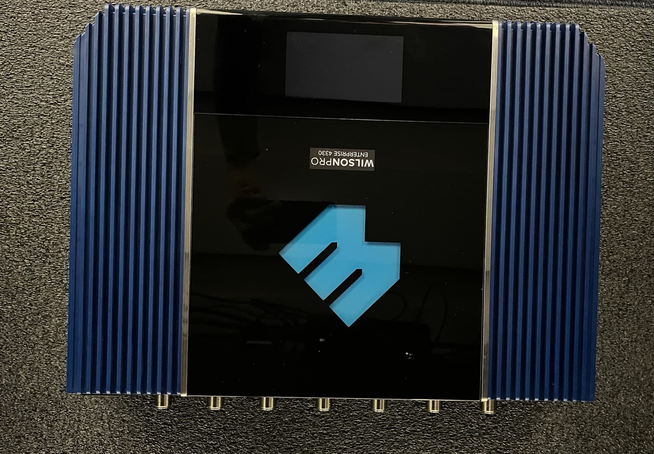
PWO075
Jan 10, 2024Quint Band Signal Booster
Equipment Class
B2W - Part 20 Wideband Consumer Booster (CMRS)
PWO460061
Sep 22, 2020Quint Band Signal Booster
Equipment Class
B2W - Part 20 Wideband Consumer Booster (CMRS)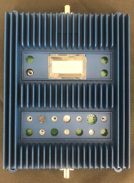
PWO460062
Aug 13, 2020Quint Band Signal Booster
Equipment Class
B2W - Part 20 Wideband Consumer Booster (CMRS)