PWO271247SBSignal Boost DT Wireless Amplifier
Wilson Electronics, LLC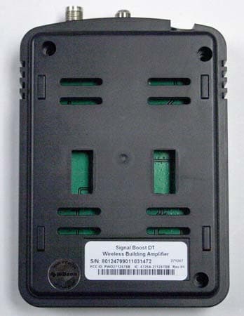
Click to zoom
Application Details
- Equipment Class
- PCB - PCS Licensed Transmitter
- Date of Grant
- Jul 17, 2007
- Application Purpose
- Original Equipment
- Date of Application
- Jul 15, 2007
- Equipment Note
- Signal Boost DT Wireless Amplifier
- Frequency Range
- 869.00000000 - 894.00000000
- Company
- Wilson Electronics, LLC
- Country
- United States
Documents & Files
Document Text
Text extracted from the exhibit documents filed with the FCC. Open a document above to read the original.
Users Manual
SIGNALBOOST™ DT Dual-Band Cellular/PCS Amplifi er System Installation Guide Contents: Guarantee and Warranty · · · · · · · · · · · · · · 1 Package Contents · · · · · · · · · · · · · · · · · · · 2 Tools Required for Installation · · · · · · · · · · 2 How It Works · · · · · · · · · · · · · · · · · · · · · · · 3 Before Getting Started · · · · · · · · · · · · · · · ·4 Reasons for Weak Cellular Signals · · · · · ·4 How to Check Your Outside Signal Strength4 Installing the Cradle Antenna · · · · · · · · · · · 5 Installing the Amplifi er Unit · · · · · · · · · · · · · 9 Powering Up the Amplifi er · · · · · · · · · · · · · 10 Understanding the Indicator Light · · · · · · · 10 Warnings and Recommendations · · · · · · · 11 Frequently Asked Questions · · · · · · · · · · ·11 About Wilson Electronics · · · · · · · · · · · · · ·12 Amplifi er Specifi cations · · · · · · · Back Cover SIGNALBOOST DT ™ DESKTOP TDDDDDDDDDDD SIGNALBOOST™ DT Installation Instructions 1 30-Day Money-Back Guarantee All Wilson Electronics products are protected by Wilson’s 30-day money-back guarantee. If for any reason the performance of any product is not acceptable, simply return the product directly to the reseller with a dated proof of purchase. 1-Year Warranty Wilson Electronics amplifi ers are warranted for one (1) year against defects in workmanship and/or materials. Warranty cases may be resolved by returning the product directly to the reseller with a dated proof of purchase. Amplifi ers may also be returned directly to the manufacturer at the consumer’s expense, with a dated proof of purchase and a Returned Material Authorization (RMA) number supplied by Wilson Electronics. Wilson shall, at its option, either repair or replace the product. Wilson Electronics will pay for delivery of the repaired or replaced product back to the original consumer. This warranty does not apply to any amplifi ers determined by Wilson Electronics to have been subjected to misuse, abuse, neglect, or mishandling that alters or damages physical or electronic properties. RMA numbers may be obtained by phoning Technical Support at 866-294-1660. Disclaimer: The information provided by Wilson Electronics, Inc. is believed to be complete and accurate. However, no responsibility is assumed by Wilson Electronics, Inc. for any business or personal losses arising from its use, or for any infringements of patents or other rights of third parties that may result from its use. Operation is subject to the following two conditions: (1) This device may not cause interference, and (2) this device must accept any interference, including interference that may cause undesired operation of this device. Copyright © 2007 Wilson Electronics, Inc. All rights reserved. Installation Instructions for the Following Wilson Amplifi er: SIGNALBOOST™ DT Dual-Band Cellular/PCS Amplifer Model # 271247, Part # 801247 FCC ID: PWO271247SB IC: 4726A-271247SB The term “IC” before the radio certifi cation number only signifi es that Industry Canada technical specifi cations were met. SIGNALBOOST™ DT Installation Instructions 2 Welcome to the Wilson Electronics Family of Products! Thank you for purchasing the Wilson SIGNALBOOST™ DT amplifi er system. You are just minutes away from enjoying improved performance from your cellular phone and/or laptop data card. When installed properly, the SIGNALBOOST™ DT will signifi cantly reduce dropped calls and improve both voice and data signal quality. By taking a few minutes to read and follow the simple instructions in this guide, you will get the most out of your new amplifi er system. If you have questions during or after installation, please don’t hesitate to contact a member of our Technical Support team by phone (866-294-1660 or 435-673- 5021) or email ([email protected]). We’re here to help! Inside this Package: SIGNALBOOST™ DT Amplifi er On-board Antenna Antenna and Cradle AC Power Supply Coaxial Cable (50 ft.) Amplifi er Wall Bracket Window-Mount (Packet A) Wall-Mount (Packet B) Pole-Mount (Packet C) Tools Required for Installation: Depending on your particular installation, you will need the following tools: • Window-mount - No additional tools needed • Wall-mount - Drill and 3/16-inch bit, Phillips-head screwdriver • Pole-mount - 1/4-inch open-end wrench or adjustable wrench SIGNALBOOST™ DT Installation Instructions 3 How it Works Your new Wilson SIGNALBOOST™ DT amplifi er system has been carefully engineered to enhance the performance of your cell phone or cellular data card. Its advanced technology is designed to signifi cantly improve voice and data signal quality and reduce disconnects and drop-outs. The SIGNALBOOST™ DT works with two antennas (included). The on-board antenna communicates with your cell phone or laptop data card, and the cradle antenna communicates with the cell tower. the cradle antenna is designed for installation inside on a window or outside on a wall or a pole, depending on your preferred confi guration. The cradle antenna collects the the outside signal and sends it through a cable to the SIGNALBOOST™ DT. The signal is then boosted and sent to the on-board antenna, which communicates with your cell phone or data card. When the cell phone or data card transmits, the on-board antenna picks up the signal and sends it to the amplifi er where it is boosted and sent through the cradle antenna to the cell tower. Note: While the SIGNALBOOST™ DT is designed to give you reliable signal improvement with the included antennas, Wilson offers a variety of optional antennas and accessories that enable you to customize your SIGNALBOOST™ DT to your specifi c needs. Visit www.wilsonelectronics.com for details. Window Installation (A)Wall Installation (B)Pole Installation (C) Antenna Option A (indoor) Cradle Window Mount Antenna Option B (outdoor) Cradle Wall Mount Antenna Option C (outdoor) Cradle Pole Mount Wireless Amplifier Area Needing Increased Signal Cell Tower Antenna and Cradle Cell Tower Antenna and Cradle…
Text truncated - open the document above for the full version.
External Photos
Bottom End Bottom Left Side Right Side Top End with Connectors Top
ID Label/Location Info
Proposed FCC ID Label Proposed Location
Internal Photos
Open Cover Top Board Bottom Board
Parts List/Tune Up Info
WILSON ELECTRONICS, INC. FCC ID: PWO271247SB PARTS LIST All of the information that would be on a parts list (component values, part no. of active devices, etc.) is in the schematic diagram, so we don't have a separate parts list.
Parts List/Tune Up Info
WILSON ELECTRONICS, INC. FCC ID: PWO271247SB TUNING PROCEDURE – No tuning procedure is available or required for this device. There is no tuning required.
Test Report
FCC PART 22H AND PART 24E TEST REPORT Applicant Wilson Electronics, Inc. Address 3301 E. Deseret Drive St. George, Utah 84790 USA FCC ID PWO271247SB IC Label IC: 4726A-271247SB Model Number 271247 Product Description Signal Boost DT Wireless Amplifier Date Sample Received May 29, 2007 Date Tested May 29, 2007 Tested By Nam Nguyen Approved By Mario de Aranzeta Report No. 2180AUT7TestReport.pdf Test Results PASS FAIL THE ATTACHED REPORT SHALL NOT BE REPRODUCED EXCEPT IN FULL WITHOUT THE WRITTEN APPROVAL OF TIMCO ENGINEERING, INC. 849 NW STATE ROAD 45 NEWBERRY, FL 32669 USA PH: 888.472.2424 OR 352.472.5500 FAX: 352.472.2030 EMAIL: [email protected] HTTP://WWW.TIMCOENGR.COM Certificate # 0955-01 APPLICANT: WILSON ELECTRONICS, INC. FCC ID: PWO271247SB, IC: 4726A-271247SB Repot #:C:\Ready_To_Convert\Doc\816863.DOC Page 2 of 61 TABLE OF CONTENTS ATTESTATION STATEMENT ............................................................................ 4 REPORT SUMMARY ........................................................................................ 5 TEST ENVIRONMENT ..................................................................................... 5 TEST SETUP ................................................................................................... 5 DEVICE UNDER TEST INFORMATION ............................................................ 6 EQUIPMENT LIST ........................................................................................... 7 TEST PROCEDURE ......................................................................................... 8 RF POWER OUTPUT........................................................................................ 11 Test Data Table 1 – Output Power – CDMA 1900 – Uplink/Downlink....... 11 Test Data Table 2 – Output Power – EDGE 1900 – Uplink/Downlink ....... 11 Test Data Table 3 – Output Power – GSM 1900 – Uplink/Downlink ......... 11 Test Data Table 5 – Output Power – CDMA 800 – Uplink/Downlink......... 12 Test Data Table 6 – Output Power – EDGE 800 – Uplink/Downlink ......... 12 Test Data Table 7 – Output Power – GSM 800 – Uplink/Downlink ........... 12 Test Data Table 8 – Output Power – AMPS 800 – Uplink/Downlink ......... 12 INPUT/OUTPUT MODULATED AMPLITUDE COMPARISON AND BAND-EDGES COMPLIANCE ............................................................................................... 13 Test Data Table 10 – CDMA 1900 – Uplink/Downlink......................................... 14 Figure 1: CDMA – In vs. Out 1851.25MHz ............................................... 14 Figure 2: CDMA – In vs. Out 1908.75MHz ............................................... 15 Figure 3: CDMA – In vs. Out 1931.25MHz ............................................... 16 Figure 4: CDMA – In vs. Out 1988.75MHz ............................................... 17 Test Data Table 11 – EDGE 1900 – Uplink/Downlink ......................................... 18 Figure 5: EDGE – In vs. Out 1850.20MHz ............................................... 18 Figure 6: EDGE – In vs. Out 1909.80MHz ............................................... 19 Figure 7: EDGE – In vs. Out 1930.20MHz ............................................... 20 Figure 8: EDGE – In vs. Out 1989.80MHz ............................................... 21 Test Data Table 12 –GSM 1900 – Uplink/Downlink ............................................ 22 Figure 9: GSM – In vs. Out 1850.20MHz ................................................. 22 Figure 10: GSM – In vs. Out 1909.80MHz ............................................... 23 Figure 11: GSM – In vs. Out 1930.20MHz ............................................... 24 Figure 12: GSM – In vs. Out 1989.80MHz ............................................... 25 Test Data Table 13 – CDMA 800 – Uplink/Downlink........................................... 26 Figure 13: CDMA – In vs. Out 825.25MHz ............................................... 26 Figure 14: CDMA – In vs. Out 847.75 MHz .............................................. 27 Figure 15: CDMA – In vs. Out 870.25 MHz .............................................. 28 Figure 16: CDMA – In vs. Out 892.75 MHz .............................................. 29 Test Data Table 14 – EDGE 800 – Uplink/Downlink ........................................... 30 Figure 17: EDGE – In vs. Out 824.20 MHz .............................................. 30 Figure 18: EDGE – In vs. Out 848.80 MHz .............................................. 31 Figure 19: EDGE – In vs. Out 869.20 MHz .............................................. 32 Figure 20: EDGE – In vs. Out 893.80 MHz .............................................. 33 APPLICANT: WILSON ELECTRONICS, INC. FCC ID: PWO271247SB, IC: 4726A-271247SB Repot #:C:\Ready_To_Convert\Doc\816863.DOC Page 3 of 61 Test Data Table 15 – GSM 800 – Uplink/Downlink ............................................. 34 Figure 21: GSM – In vs. Out 824.2 MHz .................................................. 34 Figure 22: GSM – In vs. Out 848.8 MHz .................................................. 35 Figure 23: GSM – In vs. Out 869.2MHz ................................................... 36 Figure 24: GSM – In vs. Out 893.8MHz ................................................... 37 Test Data Table 16 – AMPS 800 – Uplink/Downlink ........................................... 38 Figure 25: AMPS – In vs. Out 824.20 MHz............................................... 38 Figure 26: AMPS – In vs. Out 848.80 MHz............................................... 39 Figure 27: AMPS – In vs. Out 869.20 MHz............................................... 40 Figure 28: AMPS – In vs. Out 893.80 MHz............................................... 41 INTERMODULATION PRODUCT SPURIOUS EMISSIONS ............................... 42 Figure 29: CDMA 3 tones intermodulation - (1850 – 1910) MHz. ............. 43 Figure 30: CDMA 3 tones intermodulation - (1930 – 1990) MHz. ............. 44 Figure 31: CDMA 3 tones intermodulation – (824 – 849) MHz. .…
Text truncated - open the document above for the full version.
Test Report
FCC PART 22H AND PART 24E TEST REPORT Applicant Wilson Electronics, Inc. Address 3301 E. Deseret Drive St. George, Utah 84790 USA FCC ID PWO271247SB IC Label IC: 4726A-271247SB Model Number 271247 Product Description Signal Boost DT Wireless Amplifier Date Sample Received May 29, 2007 Date Tested May 29, 2007 Tested By Nam Nguyen Approved By Mario de Aranzeta Report No. 2180AUT7TestReport.pdf Test Results PASS FAIL THE ATTACHED REPORT SHALL NOT BE REPRODUCED EXCEPT IN FULL WITHOUT THE WRITTEN APPROVAL OF TIMCO ENGINEERING, INC. 849 NW STATE ROAD 45 NEWBERRY, FL 32669 USA PH: 888.472.2424 OR 352.472.5500 FAX: 352.472.2030 EMAIL: [email protected] HTTP://WWW.TIMCOENGR.COM Certificate # 0955-01 APPLICANT: WILSON ELECTRONICS, INC. FCC ID: PWO271247SB, IC: 4726A-271247SB Repot #:W:\W\WILSON_PWO\2180AUT7\2180AUT7TestReport.doc Page 2 of 61 TABLE OF CONTENTS ATTESTATION STATEMENT ............................................................................ 4 REPORT SUMMARY ........................................................................................ 5 TEST ENVIRONMENT ..................................................................................... 5 TEST SETUP ................................................................................................... 5 DEVICE UNDER TEST INFORMATION ............................................................ 6 EQUIPMENT LIST ........................................................................................... 7 TEST PROCEDURE ......................................................................................... 8 RF POWER OUTPUT........................................................................................ 11 Test Data Table 1 – Output Power – CDMA 1900 – Uplink/Downlink....... 11 Test Data Table 2 – Output Power – EDGE 1900 – Uplink/Downlink ....... 11 Test Data Table 3 – Output Power – GSM 1900 – Uplink/Downlink ......... 11 Test Data Table 5 – Output Power – CDMA 800 – Uplink/Downlink......... 12 Test Data Table 6 – Output Power – EDGE 800 – Uplink/Downlink ......... 12 Test Data Table 7 – Output Power – GSM 800 – Uplink/Downlink ........... 12 Test Data Table 8 – Output Power – AMPS 800 – Uplink/Downlink ......... 12 INPUT/OUTPUT MODULATED AMPLITUDE COMPARISON AND BAND-EDGES COMPLIANCE ............................................................................................... 13 Test Data Table 10 – CDMA 1900 – Uplink/Downlink......................................... 14 Figure 1: CDMA – In vs. Out 1851.25MHz ............................................... 14 Figure 2: CDMA – In vs. Out 1908.75MHz ............................................... 15 Figure 3: CDMA – In vs. Out 1931.25MHz ............................................... 16 Figure 4: CDMA – In vs. Out 1988.75MHz ............................................... 17 Test Data Table 11 – EDGE 1900 – Uplink/Downlink ......................................... 18 Figure 5: EDGE – In vs. Out 1850.20MHz ............................................... 18 Figure 6: EDGE – In vs. Out 1909.80MHz ............................................... 19 Figure 7: EDGE – In vs. Out 1930.20MHz ............................................... 20 Figure 8: EDGE – In vs. Out 1989.80MHz ............................................... 21 Test Data Table 12 –GSM 1900 – Uplink/Downlink ............................................ 22 Figure 9: GSM – In vs. Out 1850.20MHz ................................................. 22 Figure 10: GSM – In vs. Out 1909.80MHz ............................................... 23 Figure 11: GSM – In vs. Out 1930.20MHz ............................................... 24 Figure 12: GSM – In vs. Out 1989.80MHz ............................................... 25 Test Data Table 13 – CDMA 800 – Uplink/Downlink........................................... 26 Figure 13: CDMA – In vs. Out 825.25MHz ............................................... 26 Figure 14: CDMA – In vs. Out 847.75 MHz .............................................. 27 Figure 15: CDMA – In vs. Out 870.25 MHz .............................................. 28 Figure 16: CDMA – In vs. Out 892.75 MHz .............................................. 29 Test Data Table 14 – EDGE 800 – Uplink/Downlink ........................................... 30 Figure 17: EDGE – In vs. Out 824.20 MHz .............................................. 30 Figure 18: EDGE – In vs. Out 848.80 MHz .............................................. 31 Figure 19: EDGE – In vs. Out 869.20 MHz .............................................. 32 Figure 20: EDGE – In vs. Out 893.80 MHz .............................................. 33 APPLICANT: WILSON ELECTRONICS, INC. FCC ID: PWO271247SB, IC: 4726A-271247SB Repot #:W:\W\WILSON_PWO\2180AUT7\2180AUT7TestReport.doc Page 3 of 61 Test Data Table 15 – GSM 800 – Uplink/Downlink ............................................. 34 Figure 21: GSM – In vs. Out 824.2 MHz .................................................. 34 Figure 22: GSM – In vs. Out 848.8 MHz .................................................. 35 Figure 23: GSM – In vs. Out 869.2MHz ................................................... 36 Figure 24: GSM – In vs. Out 893.8MHz ................................................... 37 Test Data Table 16 – AMPS 800 – Uplink/Downlink ........................................... 38 Figure 25: AMPS – In vs. Out 824.20 MHz............................................... 38 Figure 26: AMPS – In vs. Out 848.80 MHz............................................... 39 Figure 27: AMPS – In vs. Out 869.20 MHz............................................... 40 Figure 28: AMPS – In vs. Out 893.80 MHz............................................... 41 INTERMODULATION PRODUCT SPURIOUS EMISSIONS ............................... 42 Figure 29: CDMA 3 tones intermodulation - (1850 – 1910) MHz. ............. 43 Figure 30: CDMA 3 tones intermodulation - (1930 – 1990) MHz. ............. 44 Figure 31: CDMA 3 tones intermodul…
Text truncated - open the document above for the full version.
Contact Information
Applicant
Ilesh Patel(Senior RF Design Engineer)
Test Firm
Timco Engineering, Inc.Sid Sanders
Technical Specifications
| # | Rule Parts | Frequency Range | Power Output | Emission | Tolerance |
|---|---|---|---|---|---|
| 14 | 22H | 869 MHz - 894 MHz | 17.00 mW | F1D | Amp |
Other Applications from Wilson Electronics, LLC
PWO086
Mar 09, 2026Single Band Bi-Directional Amplifier
Equipment Class
B2W - Part 20 Wideband Consumer Booster (CMRS)PWO072
Aug 26, 20245G NR Industrial Signal Booster
Equipment Class
B2I - Part 20 Industrial Booster (CMRS)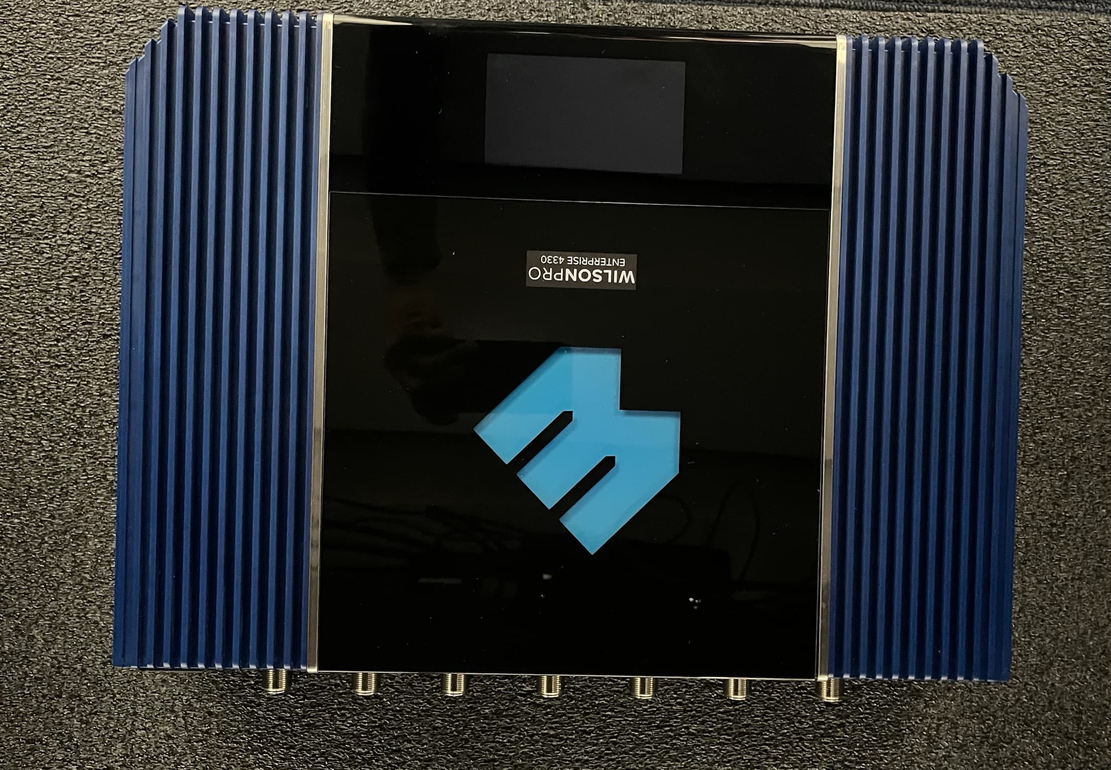
PWO075
Jan 10, 2024Quint Band Signal Booster
Equipment Class
B2W - Part 20 Wideband Consumer Booster (CMRS)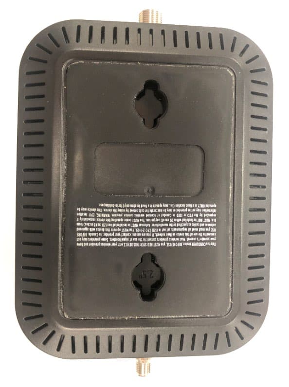
PWO460065
Nov 04, 2020Dual Band Signal Booster
Equipment Class
B2W - Part 20 Wideband Consumer Booster (CMRS)
PWO460061
Sep 22, 2020Quint Band Signal Booster
Equipment Class
B2W - Part 20 Wideband Consumer Booster (CMRS)