PWO276215DUAL-BAND CHANNELIZED SIGNAL BOOSTER
Wilson Electronics, LLC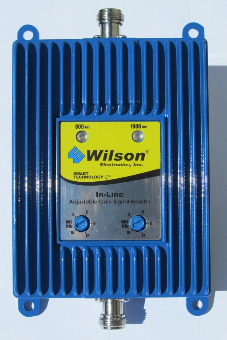
Click to zoom
Application Details
- Equipment Class
- AMP - Amplifier
- Date of Grant
- Apr 03, 2012
- Application Purpose
- Original Equipment
- Date of Application
- Apr 03, 2012
- Equipment Note
- DUAL-BAND CHANNELIZED SIGNAL BOOSTER
- Frequency Range
- 1930.00000000 - 1990.00000000
- Company
- Wilson Electronics, LLC
- Country
- United States
Documents & Files
Document Text
Text extracted from the exhibit documents filed with the FCC. Open a document above to read the original.
Users Manual
Wilson ® Electronics, Inc. Contents: Quick Install Overview . . . . . . . . . . . . . . . . . . . . . . . . . . . . . .2 Installation Diagram . . . . . . . . . . . . . . . . . . . . . . . . . . . . . . . .3 Understanding the Signal Booster Lights . . . . . . . . . . . . . . . 9 Warnings and Recommendations . . . . . . . . . . . . . . . . . . . .11 Note: This manual contains important safety and operating information . Please read and follow the instructions in this manual . Failure to do so could be hazardous and result in damage to your Signal Booster . In-Line 17dB Adjustable Gain 800/1900 MHz Smart Technology ™ Signal Booster Appearance of device and accessories may vary . 1 Contact Wilson Electronics Technical Support Team with any questions at 866-294-1660 or email: [email protected]. Mon.- Fri. Hours: 7 am to 6 pm MST. 2 Installation Instructions for the Following Wilson Signal Booster: In-Line, 17dB Adjustable Gain 800/1900 MHz Smart Technology ™ Signal Booster Model # 276215 FCC ID: PWO276215 IC: 4726A-276215 The term “IC” before the radio certification number only signifies that Industry Canada technical specifications were met . How it Works Wilson Electronics Signal Boosters are bi-directional devices that deliver service levels consistent with what would be expected in areas of high cell network coverage . They amplify a weak or shadowed signal in mobile, marine and in-building applications . When using a Wilson Electronics Signal Booster in conjunction with Wilson Electronics antennas, the Outside Antenna will collect the cell tower signal and send it through the cable to the Signal Booster . The signal is then amplified and re- transmitted through the Inside Antenna into the room . Cell phones and cellular data cards in that area then communicate with the improved signal . When a cell phone or cellular device transmits, the signal is received by the Inside Antenna, amplified by the Signal Booster and broadcasted back to the cell tower through the Outside Antenna . The In-Line Signal Booster (806215) is designed to offset cable and splitter/tap loss for in-building installations . It should be used on the Inside Antenna side of a Wilson Electronics In-Building Signal Booster such as the AG Pro 75 . Inside this Package In-Line Signal Booster (806215) AC/DC Power Supply To purchase, call Wilson Electronics Sales Department at: 800-204-4104 Indoor Antenna Option Splitter OptionsTap Option Wide-Band Panel Antenna 700-2700MHz (301135 50 ohm, 301155 75 ohm, 304451 50 ohm, 304452, 304453, 304471 75 ohm, 304472, 304473) Note: Kits may contain different accessories 2-Way (859957) 3-Way (859980) 4-Way (859981) (859907) Appearance of device and accessories may vary . 1 2 Contact Wilson Electronics Technical Support Team with any questions at 866-294-1660 or email: [email protected]. Mon.- Fri. Hours: 7 am to 6 pm MST. 1 . Install In-Building Signal Booster (such as the AG Pro 75 sold separately) . Use the installation guide for the model you purchased to install . 2 . Select a location to install the In-Line Signal Booster that is away from excessive heat, direct sunlight, moisture and has proper ventilation . Do not place the Signal Booster in an air-tight enclosure . 3 . The In-Line Signal Booster should be placed where it can make up for installation gain loss due to cable, taps or splitters . Optimal location is near or directly connected to the Inside Antenna . 4 . a) Connect a cable to the in-building Signal Booster at the connector labeled “Inside Antenna .” b) Run the cable to the In-Line Signal Booster, attach to the connector labeled “Outside Antenna .” c) From the In-Line Signal Booster connector marked “Inside Antenna” run a cable to the Inside Antenna . For more information on running cable (see diagram on pages 3 & 4) . 5 . Before powering up the In-Line Signal Booster, verify that all cables are connected and check that all connections are tight . Note: Be careful when plugging the connectors in so as not to bend the center pins on the connectors (see page 7) . 6 . The In-Line Signal Booster has been packaged with the gain control knobs adjusted to the highest gain position . If one or both of the lights are not green (see pages 9 & 10) . Quick Install Overview See Installation Diagram on page 3 . Contact Wilson Electronics Technical Support Team with any questions at 866-294-1660 . Warning: Connecting the Signal Booster directly to a cell phone with use of an adapter may damage the cell phone and/or the Signal Booster . 3 Contact Wilson Electronics Technical Support Team with any questions at 866-294-1660 or email: [email protected]. Mon.- Fri. Hours: 7 am to 6 pm MST. 4 Typical Installation Outside Antenna Inside Antenna Potential In-Line (806215) location Installation Diagram Inside Antenna Preferred Method: Place the Inside Antenna in the ceiling facing down for the best coverage . Note: A Lightning Surge Protector is recommended for all building installations (sold separately). Make sure the protector is installed in line between the Outside Antenna and the Signal Booster. (Optional second antenna for additional coverage). Null Zone: The area under the Outside Antenna, where the Outside Antenna radiates the least . Note: The Inside Antenna may be mounted on the wall directly under the Outside Antenna, in the null zone, if 20 feet of vertical separation can be maintained. Note: Do not install the In-Line without an In-Building Signal Booster between the Outside Antenna and In-Line. Note: Install the In-Line close as possible to Inside Antenna for optimal performance. 3 4 Contact Wilson Electronics Technical Support Team with any questions at 866-294-1660 or email: [email protected]. Mon.- Fri. Hours: 7 am to 6 pm MST. Before Getting Started This guide will help you properly install your Wilson Electronics Signal Booster . It is important to read through all of the installation steps for your particular application prior to installi…
Text truncated - open the document above for the full version.
Cover Letter(s)
$wils,on' 3301 East Deseret Drive St. George, Utah 84790 H#dJ'",.T"i,3:ff l:::.:'# Phone 800.204.4104 . Fax 435.656.2432 January 4,2012 Subject: Authorized lndividuals Re: FCC lD: PWO276215 To Whom lt May Concern: Please be advised that l, James W. Wilson, as contact of record in the Grantee Code data base, have designated Mr. Richard Kline of Wilson Electronics and Mr. Mario de Aranzeta of Timco Engineering as the persons responsible for the above referenced Wilson Electronics certificate application. Any and all acts carried out by Mr. Richard Kline or Mr. Mario de Aranzeta in matters pertaining to processes required in the FCC approval shall have the same legal authority as acts and communications by the undersigned. They are authorized to respond to any future issues or FCC requests regarding this project. This authorization is limited to the product referenced above. Please send any query, acknowledgement or response to this letter directly to Wilson Electronics. Sincerely, 0 )t,'--1.d*Q '^ c James W. Wilson President
Cover Letter(s)
January 4, 2012 Federal Communications Commission 7435 Oakland Mills Road Columbia, MD 21046 Subject: Data Confidentiality Gentlemen: Wilson Electronics, Inc. respectfully requests confidentiality of certain documentation provided with the submission of our model 276215 Signal Booster under FCC ID: PWO276215in accordance with sections 0.457 and 0.459 of the Commission’s regulations. We request that the following documents be kept confidential: 1. Schematic Diagram (4 pages), filename: 276215 Schematic.pdf 2. Operational Description, filename: 276215 Operational Description.pdf 3. Block Diagram, filename: 276215 Block Diagram.pdf 4. Parts List (3 pages), filename: 276215 Parts List.pdf The above material is confidential and contains proprietary trade secrets and technical data which must be kept from competitors. Public access to these items could result in duplication of our circuitry and/or techniques thereby reducing our competitive advantage and causing us severe damage. Sincerely, Richard M. Kline Senior Electrical Engineer
External Photos
APPLICANT: WILSON ELECTRONICS INC. FCC ID: PWO276215 IC: 4726A-276215 MODEL: 276215 EXTERNAL PHOTOS
ID Label/Location Info
APPLICANT: WILSON ELECTRONICS INC. FCC ID: PWO276215 IC: 4726A-276215 MODEL: 276215 LABEL SAMPLE AND LOCATION
Internal Photos
APPLICANT: WILSON ELECTRONICS INC. FCC ID: PWO276215 IC: 4726A-276215 MODEL: 276215 INTERNAL PHOTOS
Parts List/Tune Up Info
March 14, 2012 Tuning and Adjustment of Wilson Model 276215 Signal Booster There are no external tuning adjustments. The installer adjusts the gain of the booster as explained in pages 10 and 11 of the User Manual. These adjustments are “fail safe” to prevent interference with cellular systems. If the adjustments are not made properly, the amplifier will either shut off or reduce its gain. Indication of these less then optimum conditions is evident by the booster’s LED indicator lights. Sincerely, Richard M. Kline Senior Electrical Engineer
RF Exposure Info
RF Radiation Safety Report APPLICANT WILSON ELECTRONICS, INC. 3301 E. DESERET DRIVE ST. GEORGE UTAH 84790 USA FCC ID PWO276215 MODEL NUMBER 276215 PRODUCT DESCRIPTION BOOSTER RADIATION SAFETY DATE SAMPLE RECEIVED 12/7/2011 DATE TESTED 01/9/2012 TESTED BY Sushant Kadimdivan APPROVED BY Mario de Aranzeta TIMCO REPORT NO. W\WILSON_PWO\2881UT11\2881UT11TestReport.doc TOTAL PAGES 9 TEST RESULTS PASS FAIL THE ATTACHED REPORT SHALL NOT BE REPRODUCED EXCEPT IN FULL WITHOUT THE WRITTEN APPROVAL OF TIMCO ENGINEERING, INC. 849 NW STATE ROAD 45 NEWBERRY, FL 32669 USA PH: 888.472.2424 OR 352.472.5500 FAX: 352.472.2030 EMAIL: [email protected] HTTP://WWW.TIMCOENGR.COM Certificate # 0955-01 Page 2 of 9 Applicant: WILSON ELECTRONICS, INC. FCC ID: PWO276215 Report: W\WILSON_PWO\2881UT11\2881UT11TestReport.doc TABLE OF CONTENTS GENERAL REMARKS ............................................................................................................. 3 GENERAL INFORMATION ...................................................................................................... 4 EQUIPMENT LIST .................................................................................................................. 5 TEST PROCEDURE ................................................................................................................ 6 REQUIREMENTS ................................................................................................................... 6 TEST DATA ............................................................................................................................ 6 CONCLUSION ........................................................................................................................ 7 TEST SETUP PICTURES ......................................................................................................... 8 TEST SAMPLE PICTURES ...................................................................................................... 9 Page 3 of 9 Applicant: WILSON ELECTRONICS, INC. FCC ID: PWO276215 Report: W\WILSON_PWO\2881UT11\2881UT11TestReport.doc GENERAL REMARKS The attached report shall not be reproduced except in full without the written permission of Timco Engineering Inc. Summary The device under test does: fulfill the general approval requirements as identified in this test report not fulfill the general approval requirements as identified in this test report Attestations This equipment has been tested in accordance with the standards identified in this test report. To the best of my knowledge and belief, these tests were performed using the measurement procedures described in this report. All instrumentation and accessories used to test products for compliance to the indicated standards are calibrated regularly in accordance with ISO 17025 requirements. Testing Certificate # 0955-01 I attest that the necessary measurements were made, under my supervision, at: Timco Engineering Inc. 849 NW State Road 45 Newberry, Fl 32669 Authorized Signatory Name: Mario de Aranzeta C.E.T. Compliance Engineer/ Lab. Supervisor Date: 01/12/2012 Tested by: Sushant Kadimdivan Signature: Page 4 of 9 Applicant: WILSON ELECTRONICS, INC. FCC ID: PWO276215 Report: W\WILSON_PWO\2881UT11\2881UT11TestReport.doc GENERAL INFORMATION DUT Specification DUT Description BOOSTER RADIATION SAFETY FCC ID PWO276215 Model Number 276215 Operating Frequency Uplink 824 – 849 MHz Downlink 869 – 894 MHz Uplink 1850 – 1910 MHz Downlink 1930 – 1990 MHz Type of Emission F9W (CDMA & WCDMA), GXW (GSM), F1D (AMPS), G7W (EDGE) Modulation CDMA, WCDMA, GSM, EDGE, FM, HSPA, EVDO, LTE DUT Power Source 110–120Vac/50– 60Hz DC Power 6 V Battery Operated Exclusively Test Item Prototype Pre-Production Production Type of Equipment Fixed Mobile Portable Test Conditions The temperature was 26ºC with a relative humidity of 50%. Modification to the DUT None Test Exercise The DUT was fed a CW signal from a signal generator Applicable Standards FCC OET BULLETIN 65 Test Facility Timco Engineering Inc. at 849 NW State Road 45 Newberry, FL 32669 USA. Supporting Peripheral Equipment: Antenna, Wilson Electronics - Model # 301135 Page 5 of 9 Applicant: WILSON ELECTRONICS, INC. FCC ID: PWO276215 Report: W\WILSON_PWO\2881UT11\2881UT11TestReport.doc EQUIPMENT LIST Device Manufacturer Model Serial Number Cal/Char Date Due Date Signal Generator HP 8648C 3847A04696 6/12/2011 6/12/2013 Amplifier Mini Circuits ZHL-42 15542 - - Power Meter/Sensor Boonton 4531/51072A 11793/34647 11/12/2010 11/12/2012 Field Monitor Amplifier Research FM5004 22288 - - Field Probe Amplifier Research FP6001 302504 04/11/11 04/11/13 Page 6 of 9 Applicant: WILSON ELECTRONICS, INC. FCC ID: PWO276215 Report: W\WILSON_PWO\2881UT11\2881UT11TestReport.doc TEST PROCEDURE The device under test consists of the Booster (model#276215) coupled with the antenna (model#301135), both manufactured by Wilson Electronics. The CW input signal to the booster was adjusted until the maximum output power of the booster was obtained. The frequency was set to the lowest frequency in the band. The lowest frequency in the band represents the least attenuation between the antenna and a person. The antenna was connected directly to the Booster and positioned at a height of 1.5 m above the ground plane. The location for the antenna was chosen in such a way that the reflection from any nearby walls and objects is minimized. The field strength was measured using an isotropic field probe. The field probe was positioned in front of the antenna and the height adjusted to maximize the field strength. The distance between the antenna and the field probe was varied in steps (from 6 cm to 30 cm) and the field strength recorded at each point. REQUIREMENTS According to the FCC OET BULLETIN 65 the maximum permissible exposure is (f/1500)mW/cm2 at 869 MHz for uncontrolled environment. The limit is 1 mW/cm2 at 1930 MHz for uncontrolled environment. TEST DATA 1) Frequency 1: 1930 MHz Antenna = model #…
Text truncated - open the document above for the full version.
Test Report
INDUSTRY CANADA RSS-131 AND FCC PART 22H AND PART 24E TEST REPORT Applicant WILSON ELECTRONICS, INC. Address 3301 E. DESERET DRIVE ST. GEORGE UTAH 84790 USA FCC ID PWO276215 IC Label IC: 4726A-276215 Model Number 276215 Product Description BIDIRECTIONAL BOOSTER Date Sample Received 10/5/2011 Date Tested 10/7/2011 Tested By Nam Nguyen Approved By Mario de Aranzeta Report No. 2304AT11TestReport.doc Test Results PASS FAIL THE ATTACHED REPORT SHALL NOT BE REPRODUCED EXCEPT IN FULL WITHOUT THE WRITTEN APPROVAL OF TIMCO ENGINEERING, INC. Test Certificate #0955-01 849 NW STATE ROAD 45 NEWBERRY, FL 32669 USA PH: 888.472.2424 OR 352.472.5500 FAX: 352.472.2030 EMAIL: [email protected] HTTP://WWW.TIMCOENGR.COM APPLICANT: WILSON ELECTRONICS, INC. FCC ID: PWO276215, IC: 4726A-276215 Report #: W\WILSON_PWO\2304AT11\2304AT11TestReport.doc Page 2 of 79 TABLE OF CONTENTS ATTESTATION STATEMENT ............................................................................ 4 REPORT SUMMARY ........................................................................................ 5 TEST ENVIRONMENT ..................................................................................... 5 TEST SETUP ................................................................................................... 5 DEVICE UNDER TEST INFORMATION ............................................................ 6 EQUIPMENT LIST ........................................................................................... 7 TEST PROCEDURE ......................................................................................... 8 RF POWER OUTPUT ..................................................................................... 11 Test Data Table 1 – Output Power – CDMA 1900 – Uplink/Downlink .................. 11 Test Data Table 2 – Output Power – EDGE 1900 – Uplink/Downlink ................... 11 Test Data Table 3 – Output Power – GSM 1900 – Uplink/Downlink ..................... 11 Test Data Table 4 – Output Power – WCDMA 1900 – Uplink/Downlink ............... 11 Test Data Table 5 – Output Power – LTE 1900 – Uplink/Downlink ...................... 12 Test Data Table 6 – Output Power – CDMA 800 – Uplink/Downlink .................... 12 Test Data Table 7 – Output Power – EDGE 800 – Uplink/Downlink .................... 12 Test Data Table 8 – Output Power – GSM 800 – Uplink/Downlink ...................... 12 Test Data Table 9 – Output Power – WCDMA 800 – Uplink/Downlink ................. 12 Test Data Table 10 – Output Power – LTE 800 – Uplink/Downlink ...................... 13 INPUT/OUTPUT MODULATED AMPLITUDE COMPARISON AND BAND-EDGES COMPLIANCE ............................................................................................... 14 Test Data Table 11 – CDMA 1900 – Uplink/Downlink......................................... 15 Test Data Table 12– WCDMA 1900 – Uplink/Downlink ....................................... 20 Test Data Table 13 – LTE 1900 – Uplink/Downlink ............................................ 24 Test Data Table 14 – EDGE 1900 – Uplink/Downlink ......................................... 28 Test Data Table 15 –GSM 1900 – Uplink/Downlink ............................................ 32 Test Data Table 16 – CDMA 800 – Uplink/Downlink .......................................... 36 Test Data Table 17 – WCDMA 800 – Uplink/Downlink........................................ 40 Test Data Table 17 – LTE 800 – Uplink/Downlink .............................................. 44 Test Data Table 18 – EDGE 800 – Uplink/Downlink ........................................... 48 Test Data Table 19 – GSM 800 – Uplink/Downlink ............................................. 52 INTERMODULATION PRODUCT SPURIOUS EMISSIONS ............................... 56 SPURIOUS EMISSIONS AT ANTENNA TERMINALS ........................................ 65 Test Data Table 20 – Conducted Emissions – CDMA 1900 – Uplink ..................... 65 Test Data Table 21 – Conducted Emissions – CDMA 1900 – Downlink ................ 65 Test Data Table 22 – Conducted Emissions – GSM 1900 - Uplink ....................... 66 Test Data Table 23 – Conducted Emissions – GSM 1900 - Downlink ................... 66 Test Data Table 24 – Conducted Emissions – CDMA 800 - Uplink ...................... 66 Test Data Table 25 – Conducted Emissions – CDMA 800 - Downlink ................... 67 Test Data Table 26 – Conducted Emissions – GSM 800 – Uplink ......................... 67 APPLICANT: WILSON ELECTRONICS, INC. FCC ID: PWO276215, IC: 4726A-276215 Report #: W\WILSON_PWO\2304AT11\2304AT11TestReport.doc Page 3 of 79 Test Data Table 27 – Conducted Emissions – GSM 800 - Downlink ..................... 67 OUT OF BAND REJECTION: FREQUENCY RESPONSE ................................. 68 FIELD STRENGTH OF SPURIOUS EMISSIONS .............................................. 72 Test Data Table 28 – Radiated Emissions – CW (800 MHz) – Uplink /Downlink ... 72 Test Data Table 29 – Radiated Emissions – CW (1900 MHz) – Uplink /Downlink . 73 MEAN OUTPUT POWER FOR MULTI-CHANNEL ENHANCER (FOR IC ONLY) . 74 PASSBAND GAIN AND BANDWIDTH (FOR IC ONLY) ..................................... 76 APPLICANT: WILSON ELECTRONICS, INC. FCC ID: PWO276215, IC: 4726A-276215 Report #: W\WILSON_PWO\2304AT11\2304AT11TestReport.doc Page 4 of 79 ATTESTATION STATEMENT Summary The device under test does: fulfill the general approval requirements as identified in this test report not fulfill the general approval requirements as identified in this test report This equipment has been tested in accordance with the standards identified in this test report. To the best of my knowledge and belief, these tests were performed using the measurement procedures described in this report. All instrumentation and accessories used to test products for compliance to the indicated standards are calibrated regularly in accordance with ISO 17025:2005 requirements. Certificate # 0955-01 I attest that the necessary measurements were made, under my supervision, at TIM…
Text truncated - open the document above for the full version.
Contact Information
Applicant
Mikel Parry(Compliance Manager)
Test Firm
Timco Engineering, Inc.Bruno Clavier
Technical Specifications
| # | Rule Parts | Frequency Range | Power Output | Emission | Tolerance |
|---|---|---|---|---|---|
| 16 | 24E | 1.93 GHz - 1.99 GHz | 850.00 mW | G7D | Amp |
Other Applications from Wilson Electronics, LLC
PWO086
Mar 09, 2026Single Band Bi-Directional Amplifier
Equipment Class
B2W - Part 20 Wideband Consumer Booster (CMRS)PWO072
Aug 26, 20245G NR Industrial Signal Booster
Equipment Class
B2I - Part 20 Industrial Booster (CMRS)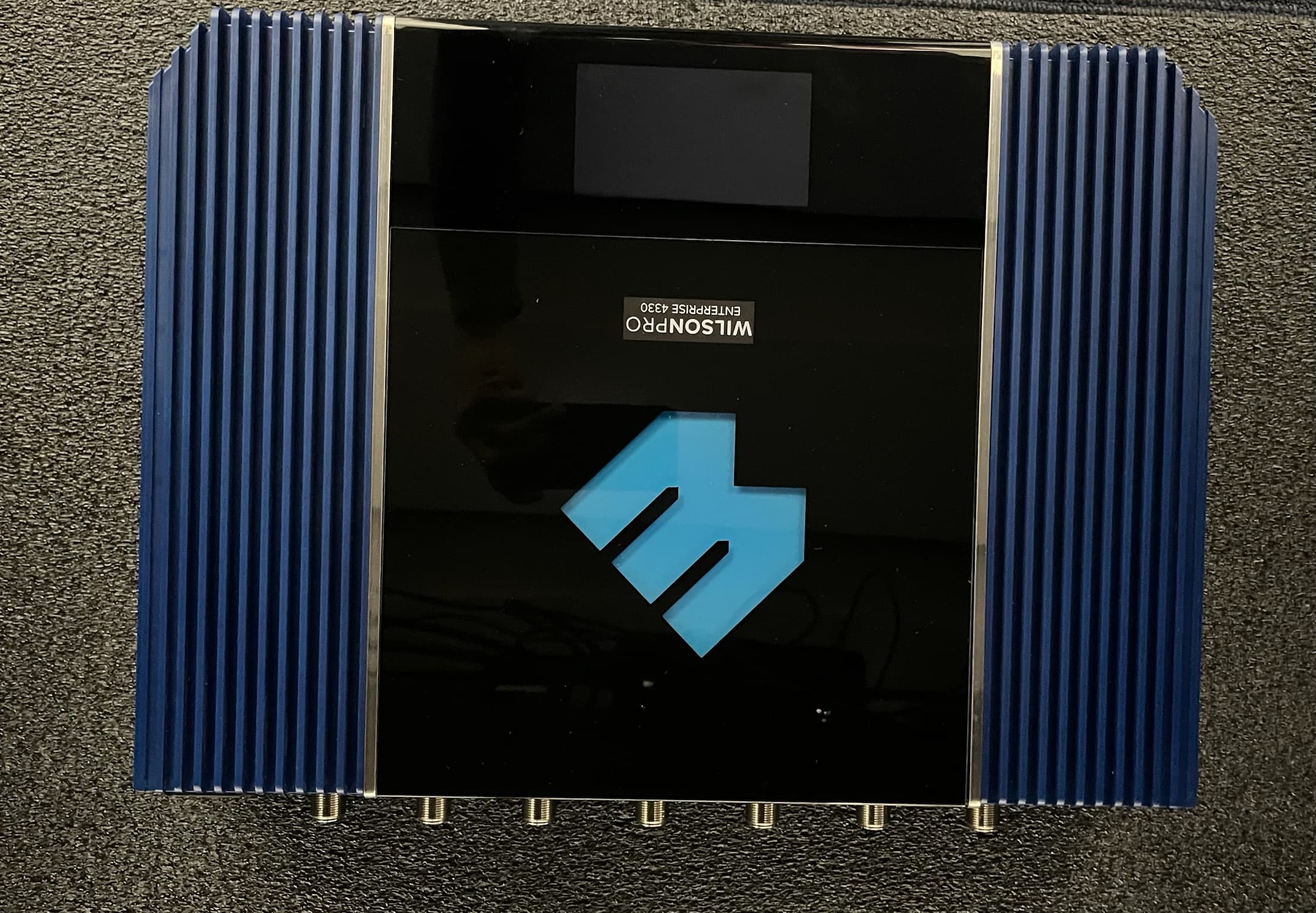
PWO075
Jan 10, 2024Quint Band Signal Booster
Equipment Class
B2W - Part 20 Wideband Consumer Booster (CMRS)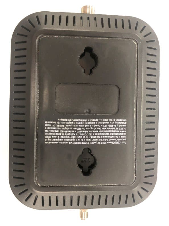
PWO460065
Nov 04, 2020Dual Band Signal Booster
Equipment Class
B2W - Part 20 Wideband Consumer Booster (CMRS)
PWO460061
Sep 22, 2020Quint Band Signal Booster
Equipment Class
B2W - Part 20 Wideband Consumer Booster (CMRS)