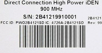
PWO2B4121SDiDEN 900 MHz Amplifier
Wilson Electronics, LLC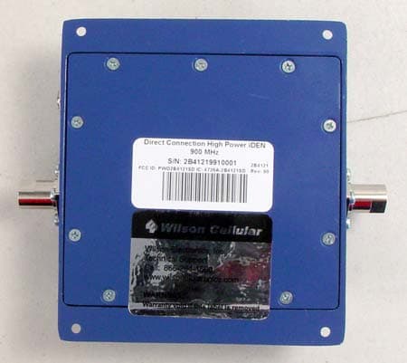
Click to zoom
Application Details
- Equipment Class
- AMP - Amplifier
- Date of Grant
- Feb 26, 2007
- Application Purpose
- Original Equipment
- Date of Application
- Feb 25, 2007
- Equipment Note
- iDEN 900 MHz Amplifier
- Frequency Range
- 935.00000000 - 940.00000000
- Company
- Wilson Electronics, LLC
- Country
- United States
Documents & Files
Document Text
Text extracted from the exhibit documents filed with the FCC. Open a document above to read the original.
Users Manual
AmplifierAmplifier Installation Guide stallatiostallat Direct Connection High Power iDEN Amplifi er 900 MHz Band Contents: Guarantee and Warranty · · · · · · · · · · · · · · · · · · · · · · · · 1 Before Getting Started / How it Works · · · · · · · · · · · · · · 3 Installing a Wilson Outside Antenna - In-Vehicle · · · · · · 4 Installing a Wilson Amplifi er - In-Vehicle · · · · · · · · · · · · 5 Installing a Wilson External Adapter - In-Vehicle · · · · · · 6 Installing a Wilson Outside Antenna - In-Building · · · · · 7 Installing a Wilson Amplifi er - In-Building · · · · · · · · · · · · 7 Installing a Wilson External Adapter - In-Building · · · · · 8 Powering Up a Wilson Amplifi er · · · · · · · · · · · · · · · · · · · 9 Warnings and Recommendations · · · · · · · · · · · · · · · · · 10 Amplifi er Specifi cations · · · · · · · · · · · · · · · · · Back Cover Wilson ® Electronics, Inc. Warning: This manual contains important safety and operating information. Please read and follow the instructions in this manual. Failure to do so could be hazardous and result in damage to your amplifi er. ! 1 30-Day Money-Back Guarantee All Wilson Electronics products are protected by Wilson’s 30-day money-back guarantee. If for any reason the performance of any product is not acceptable, simply return the product directly to the reseller with a dated proof of purchase. 1-Year Warranty Wilson Electronics amplifi ers are warranted for one (1) year against defects in workmanship and / or materials. Warranty cases may be resolved by returning the product directly to the reseller with a dated proof of purchase. Amplifi ers may also be returned directly to the manufacturer at the consumer’s expense, with a dated proof of purchase and a Returned Material Authorization (RMA) number supplied by Wilson Electronics. Wilson shall, at its option, either repair or replace the product. Wilson Electronics will pay for delivery of the repaired or replaced product back to the original consumer. This warranty does not apply to any amplifi ers determined by Wilson Electronics to have been subjected to misuse, abuse, neglect, or mishandling that alters or damages physical or electronic properties. RMA numbers may be obtained by phoning Technical Support at 866-294-1660. The Manufacturer’s rated output power of this equipment is for single carrier operation. Operation is subject to the following two conditions: (1) This device may not cause interference, and (2) this device must accept any interference, including interference that may cause undesired operation of this device. Disclaimer: The information provided by Wilson Electronics, Inc. is believed to be complete and accurate. However, no responsibility is assumed by Wilson Electronics, Inc. for any business or personal losses arising from its use, or for any infringements of patents or other rights of third parties that may result from its use. Copyright © 2007 Wilson Electronics, Inc. All rights reserved. 2 Installation Instructions for the Following Wilson Amplifi er Direct Connection High Power iDEN Amplifi er – Model #2B4121, Part #814121 Designed specifi cally for the iDEN 900 MHz band. FCC ID: PWO2B4121SD IC: 4726A-2B4121SD The term “IC” before the radio certifi cation number only signifi es that Industry Canada technical specifi cations were met. Antenna Options and Accessories Magnet Mount Quad-Band NMO Mount Quad-Band Glass Mount Quad-Band Amplifi er Hard Kit Cases 13 dB Yagi Cellular Antenna Amplifi er Soft Cases 3 Before Getting Started This guide will help you properly install Wilson’s direct connection amplifi ers in both in-vehicle and in-building applications. It is important to read through all of the installation steps for your particular application prior to installing any equipment. Read through the instructions, visualize where all the equipment will need to be installed and do a soft installation before mounting any equipment. If you do not understand the instructions in full, seek professional help, or contact Wilson Technical Support at 866-294-1660. Inside this Package • Direct connection amplifi er • DC plug-in power cable with On/Off switch • 6 ‘ extension cable • Cable wrench Additional Equipment • Outside antenna for in-vehicle or in-building use (required) (NOTE: specifi cally tuned iDEN antennas available) • Cell phone-specifi c external antenna adapter (required) • AC/DC power supply (optional – for in-building use) How it Works Wilson amplifi ers are small, portable, bi-directional devices that deliver service levels consistent with what would be expected in areas of high cell network coverage. They amplify a weak or shadowed signal in mobile, marine and in- building applications. When using a Wilson amplifi er in conjunction with Wilson antennas, the outside antenna will collect the cell tower signal and send it through the cable to the amplifi er. Cell phones and cellular data cards (laptops) then communicate with the improved signal. When a cell phone or cellular data card transmits, the signal is amplifi ed by the amplifi er and broadcast back to the cell tower through the outside antenna. 6‘ extension cable Direct connection amplifi er DC plug-in power cable Cable wrench 4 The outside antenna must be installed vertically. Signal performance will be degraded if the antenna is not vertical. The antenna cable may be run through the door to the amplifi er. For a more professional-looking installation, the antenna cable may be run under the door seal. Carefully pull down the door seal. Run the cable through the seal and push the seal back into place. This prevents constant wear and tear on the cable as the door opens and closes. The antenna cable is small enough to easily tuck under the door seal or plastic molding. Optional Magnet- Mount Antenna Shown Part #304202 Carefully Pull Down Door Seal Run Cable Under Seal Tuck Cable Under Seal Installing a Wilson Outside Antenna To receive the best cell signal, select a location in the center of the v…
Text truncated - open the document above for the full version.
Cover Letter(s)
February 6, 2007 Federal Communications Commission 7435 Oakland Mills Road Columbia, MD 21046 Subject: Data Confidentiality Gentlemen: Wilson Electronics, Inc. respectfully requests confidentiality of certain documentation provided with the submission of our model 2B4121 amplifier under FCC ID: PWO2B4121SD in accordance with sections 0.457 and 0.459 of the Commission’s regulations. We request that the following documents be kept confidential: 1. Schematic Diagram 2B4121SCHEM.JPG 2. 2B4121 Operational Description 3. 2B4121 Block Diagram The above material is confidential and contains proprietary trade secrets and technical data which must be kept from competitors. Public access to these items could result in duplication of our circuitry and/or techniques thereby reducing our competitive advantage and causing us severe damage. Sincerely, Richard M. Kline, R&D Engineer
Cover Letter(s)
Appendix A Non-Conformities for US Radio Equipment Authorization Non-Conformities FCC ID: PWO2B 4121SD (CKC CS Ref # E07-000007-01) The items listed below represent requests for information following review of this application for certification under United S tates (FCC) regulations. . Further question may arise pending review of responses to these items. OK # Non-Conformity or Co mment Submitted Response Respondent / Date of Response √ 1 Page 6 of the test report lists the emission designator as GXW but the application lists it as G7W: which is it? D7W is the correct designator for TDMA or iDENT and the test report has been amended Mary Ellen/19Feb07 2 3 4 5 6
External Photos
Top Bottom Left Side Right Side Outside Antenna Connect Inside Antenna Connect
Internal Photos
Internal - Cover Removed Board Top Board Bottom
Parts List/Tune Up Info
DC Voltages and Tune-Up Procedure 2.1033(c)(8): dc Voltages: While amplifying signals: Uplink: 12 VDC @ 2A, Downlink: 5VDC @300mA 2.1033(c)(9): Tune-up Procedure: Not apaplicable because there are no adjustments to be made by the users of the equipment. Everything is internal and factory adjusted.
RF Exposure Info
5046 Sierra Pines Dr. * Mariposa, CA 95338 * PH (209) 966-5240 * Fax (209) 742-6133 WORLDWIDE EMC – COMMERCIAL * INDUSTRIAL * MEDICAL * MILITARY * AVIONICS BREA, CA * FREMONT, CA * MARIPOSA, CA *CANYON PARK, WA Date of Report: January 19, 2007 Maximum Permissible Exposure Statement Calculations prepared for: Calculations prepared by: Randal Clark CKC Laboratories, Inc. 5046 Sierra Pines Dr. Mariposa, CA 95338 FCC ID Number:: Model Number: 2B4121 Fundamental Operating Frequency: 896-901 MHz Maximum Rated Output Power: 5 Watts Measured Output Power: 4.68 Watts Peak Conducted Maximum Antenna Gain: 5.12 dBi (Mobile Use) Power Output and Operating Frequency Information used for these calculations were from: CKC Laboratories, Test Report # Device and Antenna Operating Configuration: Equipment is designed for connection to only one cell phone for uplink. The peak to average ratio of the intrinsic duty cycle of TDMA signal is -9dB. Therefore average power output can be calculated as 36.7dBm - 9dB = 27.7dBm or 0.59 Watts conducted output power. The maximum antenna gain used with this equipment is 5.12dBi with a cable loss of 4.0dB as declared by the manufacturer which provides 28.8dBm or 0.76 Watts EIRP. Test Procedure: This equipment is evaluated in accordance with the guidelines set forth in OET Guide 65. Other Considerations: The downlink path is not investigated as the amplifier directly connects to end user equipment. 5046 Sierra Pines Dr. * Mariposa, CA 95338 * PH (209) 966-5240 * Fax (209) 742-6133 WORLDWIDE EMC – COMMERCIAL * INDUSTRIAL * MEDICAL * MILITARY * AVIONICS BREA, CA * FREMONT, CA * MARIPOSA, CA *CANYON PARK, WA MPE Calculations: MPE Limit in accordance with 1.1310: Occupational / Controlled Exposure X General Population / Uncontrolled Exposure MPE Limit = F / 1500 (mW/cm 2 ) = 0.58 (mW/cm 2 ) Note: Limit is calculated based on the lowest frequency used in the operating frequency range. 2 2 4 )/( d EIRP cmmWDensityPower π = Given: EIRP in mW and d in cm EIRP (mW) Distance (cm) Power Density (mW/cm 2 ) Result 762.08 10.23 0.579 Pass Statement of Compliance: This device demonstrates compliance under the operating conditions specified in this document. Under normal operating conditions, the antenna is designed to be installed in accordance with the manufacturer’s instructions in such a manor to maintain the minimum separation distance. The MPE calculations shown above demonstrate compliance to the provisions of 1.1310 in accordance with the guidelines of OET 65. As can be seen from the MPE results, this device passes the limits specified in 1.1310 at a distance of less than 20cm and at a output power of 0.76 Watts EIRP under normal operating conditions.
Test Report
Page 1 of 54 Report No.: FC07-005A ADDENDUM TO WILSON ELECTRONICS TEST REPORT FC07-005 FOR THE IDEN 900 MHZ AMPLIFIER, 2B4121 FCC PART 90 AND RSS-131 COMPLIANCE DATE OF ISSUE: FEBRUARY 19, 2007 PREPARED FOR: Wilson Electronics 3301 East Deseret Drive St. George, UT 84790 PREPARED BY: Mary Ellen Clayton CKC Laboratories, Inc. 5046 Sierra Pines Drive Mariposa, CA 95338 P.O. No.: IDN2B4121-1 W.O. No.: 85944 Date of test: January 12-16, 2007 Report No.: FC07-005A This report contains a total of 54 pages and may be reproduced in full only. Partial reproduction may only be done with the written consent of CKC Laboratories, Inc. The results in this report apply only to the items tested, as identified herein. Page 2 of 54 Report No.: FC07-005A TABLE OF CONTENTS Administrative Information .............................................................................................3 Approvals .........................................................................................................................3 FCC to Canada Standard Correlation Matrix...................................................................4 Conditions for Compliance ..............................................................................................4 Equipment Under Test (EUT) Description ......................................................................5 Equipment Under Test .....................................................................................................5 Peripheral Devices ...........................................................................................................5 Temperature and Humidity During Testing.....................................................................6 FCC 2.1033(c)(3) User’s Manual ....................................................................................6 FCC 2.1033(c)(4) Type of Emissions ..............................................................................6 FCC 2.1033(c)(5) Frequency Range................................................................................6 FCC 2.1033(c)(6) Operating Power.................................................................................6 FCC 2.1033(c)(7) Maximum Power Rating ....................................................................6 FCC 2.1033(c)(8) DC Voltages .......................................................................................6 FCC 2.1033(c)(9) Tune-Up Procedure ............................................................................6 FCC 2.1033(c)(10) Schematics and Circuitry Description..............................................6 FCC 2.1033(c)(11) Label and Placement ........................................................................6 FCC 2.1033(c)(12) Submittal Photos ..............................................................................6 FCC 2.1033(c)(13) Modulation Information ...................................................................6 FCC 2.1033(c)(14)/2.1046/90.205 - RF Power Output ...................................................7 RSS 131 Power Output ....................................................................................................9 FCC 2.1033(c)(14)/2.1051/90.210(j) - Spurious Emissions at Antenna Terminal..........12 FCC 2.1033(c)(14)/2.1053/90.210 - Field Strength of Spurious Radiation ....................28 Emissions Masks..............................................................................................................30 Input Plots ........................................................................................................................36 Output Plots .....................................................................................................................39 99% Bandwidth................................................................................................................40 Intermodulation Attenuation ............................................................................................43 Attenuation Of Out Of Band Signals ...............................................................................46 RSS-131 Passband Gain ..................................................................................................49 RSS-131 Pass Bandwidth ................................................................................................52 Page 3 of 54 Report No.: FC07-005A ADMINISTRATIVE INFORMATION DATE OF TEST: January 12-16, 2007 DATE OF RECEIPT: January 12, 2007 FREQUENCY RANGE TESTED: 9 kHz-10 GHz MANUFACTURER: Wilson Electronics 3301 East Deseret Drive St. George, UT 84790 REPRESENTATIVE: Riki Kline TEST LOCATION: CKC Laboratories, Inc. 5046 Sierra Pines Drive Mariposa, CA 95338 TEST METHOD: FCC Part 90, RSS-131 and RSS GEN PURPOSE OF TEST: Original Report: To demonstrate the compliance of the iDEN 900 MHz Amplifier, 2B4121 with the requirements for FCC Part 90 and RSS-131 devices. Addendum A: To revise the emissions designator on page 6. APPROVALS: Steve Behm, Director of Engineering Services QUALITY ASSURANCE:TEST PERSONNEL: Joyce Walker, Quality Assurance Administrative Manager Randy Clark, EMC Engineer Mike Wilkinson, EMC Engineer/Lab Manager Page 4 of 54 Report No.: FC07-005A FCC TO CANADA STANDARD CORRELATION MATRIX Canadian Standard Canadian Section FCC Standard FCC Section Test Description RSS 1315.4NANAExternal Controls RSS 1315.547 CFR1.1307RF Exposure RSS 1316.1NANAPassband Gain and Bandwidth RSS 1316.247 CFR90.205RF Power Output RSS 1316.3TIA/EIA603Non-Linearity (Intermodulation Attenuation) RSS 1316.447 CFR90.210Spurious Emissions Limitations RSS 1316.5NANAFrequency Stability (Band Translators) 3082A-1784962Site File No. CONDITIONS FOR COMPLIANCE No modifications to the EUT were necessary to comply. Page 5 of 54 Report No.: FC07-005A EQUIPMENT UNDER TEST (EUT) DESCRIPTION The customer declares the EUT tested by CKC Laboratories was representative of a production unit. EQUIPMENT UNDER TEST iDEN 900 MHz Amplifi…
Text truncated - open the document above for the full version.
Test Setup Photos
RF Power Test Setup Photo Direct Connect Test Setup Photos Field Strength of Spurious Radiation Test Setup Photos
Contact Information
Applicant
Ilesh Patel(Senior RF Design Engineer)
Technical Contact
CKC Laboratories, Inc.Mary Ellen Clayton
[email protected]800-500-4362
5046 Sierra Pines Drive · Mariposa, California · United States
Non-Technical Contact
CKC Laboratories, Inc.Mary Ellen Clayton
[email protected]800-500-4362
Test Firm
CKC Laboratories, Inc.Steve Behm
Technical Specifications
| # | Rule Parts | Frequency Range | Power Output | Emission | Tolerance |
|---|---|---|---|---|---|
| 2 | 9 | 935 MHz - 940 MHz | 2.00 mW | D7W | Amp |
Other Applications from Wilson Electronics, LLC
PWO086
Mar 09, 2026Single Band Bi-Directional Amplifier
Equipment Class
B2W - Part 20 Wideband Consumer Booster (CMRS)PWO072
Aug 26, 20245G NR Industrial Signal Booster
Equipment Class
B2I - Part 20 Industrial Booster (CMRS)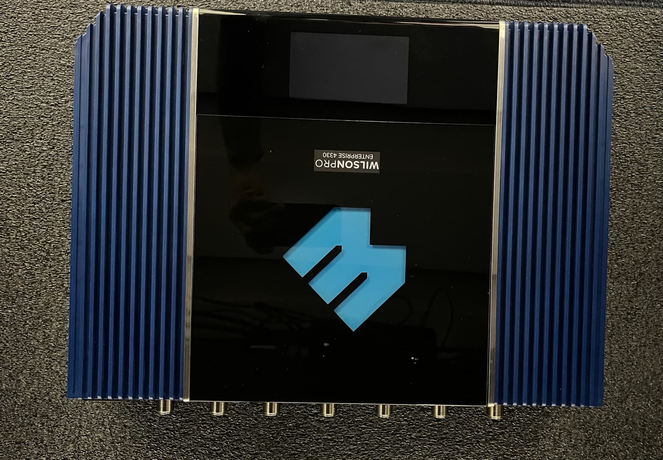
PWO075
Jan 10, 2024Quint Band Signal Booster
Equipment Class
B2W - Part 20 Wideband Consumer Booster (CMRS)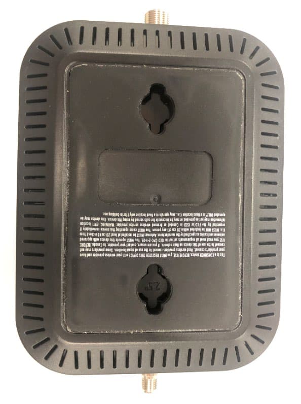
PWO460065
Nov 04, 2020Dual Band Signal Booster
Equipment Class
B2W - Part 20 Wideband Consumer Booster (CMRS)
PWO460061
Sep 22, 2020Quint Band Signal Booster
Equipment Class
B2W - Part 20 Wideband Consumer Booster (CMRS)