PWO460021Quint Band Signal Booster
Wilson Electronics, LLC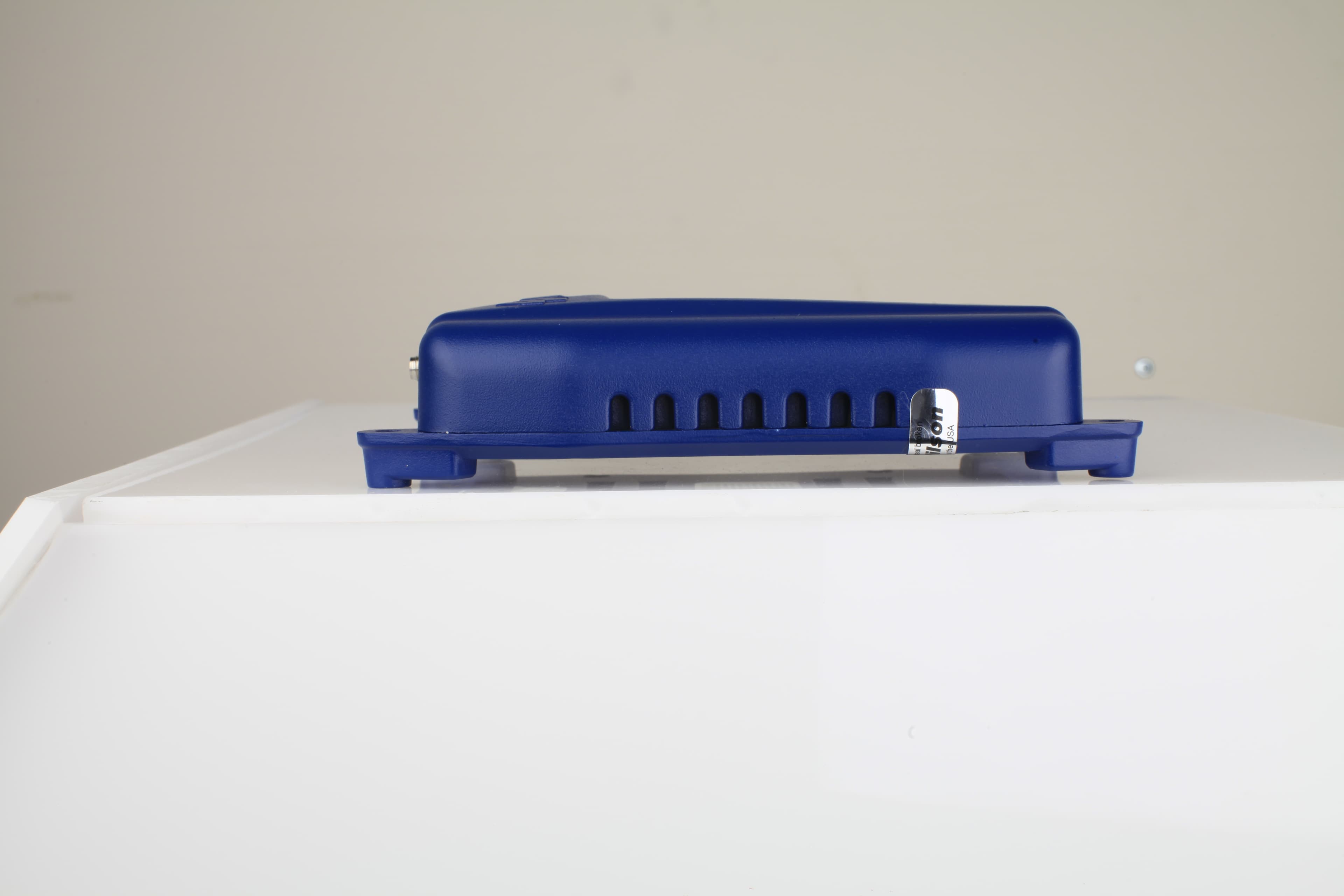
Click to zoom
Application Details
- Equipment Class
- B2W - Part 20 Wideband Consumer Booster (CMRS)
- Date of Grant
- Dec 18, 2014
- Application Purpose
- Original Equipment
- Date of Application
- Nov 24, 2014
- Equipment Note
- Quint Band Signal Booster
- Frequency Range
- 746.00000000 - 757.00000000
- Company
- Wilson Electronics, LLC
- Country
- United States
Documents & Files
Document Text
Text extracted from the exhibit documents filed with the FCC. Open a document above to read the original.
Users Manual
Need help?www.WilsonElectronics.com Tech Support 866-294-1660 Mon.- Fri. Hours: 7 am to 6 pm MST Mobile 4G ™ Cellular Signal Booster 460021 2 Need help?www.WilsonElectronics.com Tech Support 866-294-1660 Mon.- Fri. Hours: 7 am to 6 pm MST !! THE ALUMINUM CASING OF YOUR SIGNAL BOOSTER WILL ADJUST TO THE TEMPERATURE OF ITS ENVIRONMENT, BUT IS DESIGNED TO PROTECT THE SIGNAL BOOSTER TECHNOLOGY. FOR EXAMPLE, IN THE SUMMER, THE SIGNAL BOOSTER CASE MAY BE AS HOT AS 150 DEGREES INSIDE YOUR VEHICLE. THESE HIGH TEMPERATURES WILL NOT DAMAGE THE SIGNAL BOOSTER, NOR DO THEY POSE A FIRE RISK TO THE VEHICLE. AGAIN, BE SURE TO PLACE YOUR SIGNAL BOOSTER IN A LOCATION WITH ADEQUATE VENTILATION AND AWAY FROM DIRECT SUNLIGHT OR MOISTURE. THE MOBILE 4G SIGNAL BOOSTER MAY REMAIN ON, IN VEHICLES WHOSE 12V DC POWER SOURCES DO NOT AUTOMATICALLY SHUTDOWN WHEN THE VEHICLE IS TURNED OFF. THIS COULD RESULT IN DISCHARGING THE VEHICLES BATTERY IN ONE TO TWO DAYS. Installation Instructions for the Following Wilson Electronics Signal Boosters: Mobile 4G SmarTech ™ Signal Booster Model # 460021 FCC ID: PWO460021 IC: 4726A-460021 The term “IC” before the radio certification number only signifies that Industry Canada technical specifications were met. Contents Package Contents ....................................................3 Before Getting Started ................................................3 Installation ..........................................................3 Troubleshooting & Understanding Lights .................................5 Additional FAQ .......................................................6 Outside Antenna Options ..............................................7 Safety Guidelines ....................................................8 Signal Booster Specifications ..........................................9 Guarantee and Warranty ......................................Back Cover 3 Need help?www.WilsonElectronics.com Tech Support 866-294-1660 Mon.- Fri. Hours: 7 am to 6 pm MST Before Getting Started Before you install your Mobile 4G Booster and start enjoying improved cellular reception please do the following: 1. Read through all the installation steps. This will help you know what to expect from start to finish. 2. Watch the YouTube video demonstrating the Mobile 4G Signal Boost installation at: wilsonelectronics.com/ Mobile4Gvideo 3. Familiarize yourself with all materials in your product package. This will allow you to know which pieces are referenced in the instructions. Installation You can install your Mobile 4G Signal Booster in your vehicle using the following steps. NOTE: Before completing your installation, create a “soft” installation by putting the components of your Mobile 4G Signal Booster in place and testing the operation before mounting equipment. 1. Install the outside antenna. Select a location on top of the car that is: • Near the center of the vehicle’s roof. • At least 12 inches from any other antennas. • Free of obstructions. • At least 6 inches from any windows (including sunroofs). • At least 8 inches from any people. Package Contents Mobile 4G ™ Signal Booster Mini-Mag Outside Antenna 301126 Slim Low Profile Inside Antenna 301152 DC Power Supply 6V / 2A 859913 Optional Antennas 12” Mag Mount Outside Antenna 311103 NMO Outside Antenna 311104-5810 Marine Outside Antenna 311130-5810 Trucker Outside Antenna 311101 Appearance of device and accessories may vary. 4 Need help?www.WilsonElectronics.com Tech Support 866-294-1660 Mon.- Fri. Hours: 7 am to 6 pm MST The outside antenna must be installed vertically on a metallic surface. 2. Run the outside antenna cable into the car. The cable is strong enough that it may be shut in most vehicle doors without damaging the cable. For a cleaner look, carefully pull down the door seal, run the cable under the seal, and push the seal back into place. This method reduces wear on the cable as the door opens and closes. 3. Install the Low-Profile inside antenna. • Identify a place on the right side of the driver’s seat to mount the inside antenna. The location should be at least 18 inches from where the cellular device will be used. • Install the inside antenna at the same angle as the cell phone when held in use or near the laptop’s cellular data card to maximize signal strength. For a more professional look, you can install the inside antenna underneath a car seat cover or upholstery. • When you have tested the functionality of your Mobile 4G Signal Booster, mount the inside antenna by peeling off the backing of the Velcro ® and attach it to your selected location on the seat and secure the inside antenna. 4. Place and connect the Mobile 4G Signal Booster. • Select a location for the Signal Booster that is free from excessive heat, direct sunlight and moisture and that has proper ventilation. Good locations include underneath a seat or under the dashboard. • Connect the wire from the outside antenna to the port labeled “outside antenna” on the Signal Booster. • Connect the wire from the inside antenna to the port labeled “inside antenna” on the Signal Booster. • Plug the power adapter into vehicle’s 12V DC power supply and attach the cord to the side of Power Booster labeled “Power.” NOTE: Do NOT connect the power to the Signal Booster until you have connected both the inside and outside antennas. 5 Need help?www.WilsonElectronics.com Tech Support 866-294-1660 Mon.- Fri. Hours: 7 am to 6 pm MST into both the Mobile 4G Signal Booster and the power source. • If using a DC power supply in your vehicle, ensure the power supply is properly inserted. Then check the 12 volt power from the car socket and the fuse. Replace the fuse if necessary. Red light: A red light indicates oscillation is occurring. Oscillation is similar to feedback between a microphone and speaker. When oscillation occurs, the Signal Booster will power down to protect the cell tower. To eliminate oscillation, the outside antenna needs to be moved farther from the inside antenna. M…
Text truncated - open the document above for the full version.
Attestation Statements
October 17, 2014 Attestation For Wilson Signal Booster: FCC ID PWO460021 Each Signal Booster certificated under FCC ID PWO460021 is manufactured and individually tested to ensure FCC compliance: (1) Licensee consent is not required for FCC certification equipment authorization purposes, but licensee consent does remain applicable per 20.21 provisions for both provider specific and wideband boosters. (2) NPS and other compliance/safeguard features have been implemented. (3) NPS and other compliance/safeguard features are defaulted to be “On” (in operation). (4) NPS and other compliance/safeguard features cannot be field reconfigured, disabled, or removed. (5) This consumer booster is not user programmable, does not need fine tuning or adjustment, and does not require professional installation. However, in case booster indicator lights show the need, the gain may be adjusted as described in the User Manual. Such adjustments are “fail safe”, i.e., they will not enable the booster to be non-compliant to NPS or other compliance/safeguard requirements. (6) Future software upgrade will not cause non-compliance. Sincerely, Patrick L. Cook Chief Technology Officer
Cover Letter(s)
October 30, 2014 Subject: Antenna Kitting Re: FCC ID: PWO460021 To Whom It May Concern: The antenna kitting options for model 460021 signal booster were done for 46 Outside Antenna kit options and 14 Inside Antenna kit options. The order of the attached calculations is as follows: Outside Antenna Kit Options: Fixed 1. Kit 314411-40075 2. Kit 314411-5825 3. Kit 314475-0630 4. Kit 301111-0675 5. Kit 301111-5850 6. Kit 311203-40020 7. Kit 311129-400100 8. Kit 311129-5840 9. Kit 311129-0660 10. Kit 311124-0650 11. Kit 311124-400100 12. Kit 314453-5825 13. Kit 311203-5820 14. Kit 311201-0620 15. Kit 301126 16. Kit 301111-11140 17. Kit 311201-1120 18. Kit 311129-11110 19. Kit 314453-40075 20. Kit 314473-0640 21. Kit 311141-0620 22. Kit 311124-1180 23. Kit 311141-1120 24. Kit 314473-1175 25. Kit 314475-1175 26. Kit 301111-400170 27. Kit 311124-5830 Mobile 1. Kit 311703 2. Kits 311103, 311125, 311128, 314202 3. Kit 311130-5810 4. Kit 311114 5. Kit 311102 6. Kit 311104-5810 7. Kit 311701 8. Kit 311119 9. Kit 311133 10. Kit 311104-17410 11. Kit 301113 12. Kit 311112-5810 13. Kit 314203-5810 14. Kit 311112-17410 15. Kit 314203-17410 16. Kit 311101 Inside Antenna Kit Options: Mobile 1. Kit 301152 2. Kit 311106 Fixed 1. Kit 311135-40060 2. Kit 311135-5820 3. Kit 311155-0630 4. Kit 301121-40010 5. Kit 301151-0610 6. Kit 309900-50N 7. Kit 309902-75F 8. Kit 309903-75F 9. Kit 309904-75F 10. Kit 309905-50N 11. Kit 311155-1150 12. Kit 301151-1110 Sincerely, Patrick L. Cook Chief Technology Officer FCC ID: PWO460021 FCC ID: PWO460021 Final Output Power Limited to 30 dBm EIRP in all frequency bands Final Output Power Limited to 30 dBm EIRP in all frequency bands Uplink Frequency (MHz) 698 ‐ 716 777 ‐ 787 824 ‐ 849 1710 ‐ 1755 1850 ‐ 1915 Uplink Frequency (MHz) 698 ‐ 716 777 ‐ 787 824 ‐ 849 1710 ‐ 1755 1850 ‐ 1915 Uplink Output Power (dBm) 24.84 24.35 23.4 21.3 24.4 Uplink Output Power (dBm) 24.84 24.35 23.4 21.3 24.43 1 Wide Band Directional Antenna With 75' LMR 400 314411 ‐ 40075 7 Yagi Antenna 311129 With 100' LMR 400 311129 ‐ 400100 Antenna Gains (dBi) 7.3 7.2 7.8 7.9 9.1 Antenna Gains (dBi) 1.95 7.18 9.64 ‐ 6.67 ‐ 11.97 Coax Loss (dB) 2.8 3.0 3.6 4.4 5.4 Coax Loss (dB) 3.7 3.9 4.7 5.8 7.1 Final Gain less Loss (dB) 4.5 4.2 4.2 3.5 3.7 Final Gain less Loss (dB) ‐ 1.75 3.28 4.9 ‐ 12.47 ‐ 19.07 Output Power plus Final Gain (dBm EIRP) 29.34 28.55 27.6 24.8 28.1 Output Power plus Final Gain (dBm EIRP) 23.1 27.6 28.3 8.8 5.4 2 Wide Band Directional Antenna With 25' RG ‐ 58 314411 ‐ 5825 8 Yagi Antenna 311129 With 40' RG ‐ 58 311129 ‐ 5840 Antenna Gains (dBi) 7.3 7.2 7.8 7.9 9.1 Antenna Gains (dBi) 1.95 7.18 9.64 ‐ 6.67 ‐ 11.97 Coax Loss (dB) 2.9 3.1 3.2 5.1 5.4 Coax Loss (dB) 4.6 5.0 5.2 8.2 8.6 Final Gain less Loss (dB) 4.4 4.1 4.6 2.8 3.7 Final Gain less Loss (dB) ‐ 2.7 2.2 4.4 ‐ 14.9 ‐ 20.6 Output Power plus Final Gain (dBm EIRP) 29.2 28.5 28.0 24.1 28.1 Output Power plus Final Gain (dBm EIRP) 22.2 26.5 27.8 6.4 3.9 3 Wide Band Directional Antenna With 30' RG ‐ 6 314475 ‐ 0630 9 Yagi Antenna 311129 With 60' RG ‐ 6 311129 ‐ 0660 Antenna Gains (dBi) 7.3 7.2 7.8 7.9 9.1 Antenna Gains (dBi) 1.95 7.18 9.64 ‐ 6.67 ‐ 11.97 Coax Loss (dB) 3.0 3.2 3.4 5.1 5.3 Coax Loss (dB) 4.56 4.86 5.0 7.6 8.0 Final Gain less Loss (dB) 4.3 4 4.4 2.8 3.8 Final Gain less Loss (dB) ‐ 2.61 2.32 4.64 ‐ 14.29 ‐ 19.95 Output Power plus Final Gain (dBm EIRP) 29.14 28.4 27.8 24.1 28.2 Output Power plus Final Gain (dBm EIRP) 22.2 26.7 28.0 7.0 4.5 4 Yagi Antenna 301111 With 75' RG ‐ 6 301111 ‐ 0675 10 Yagi Antenna 311124 With 50' RG ‐ 6 311124 ‐ 0650 Antenna Gains (dBi) 10.0 10.0 10.8 ‐ 6.8 ‐ 13.8 Antenna Gains (dBi) ‐ 18.7 ‐ 18.7 ‐ 23.4 9.1 10.9 Coax Loss (dB) 5.7 6.075 6.3 9.525 9.975 Coax Loss (dB) 3.8 4.05 4.2 6.4 6.7 Final Gain less Loss (dB) 4.3 3.925 4.5 ‐ 16.325 ‐ 23.775 Final Gain less Loss (dB) ‐ 22.50 ‐ 22.75 ‐ 27.60 2.75 4.25 Output Power plus Final Gain (dBm EIRP) 29.14 28.3 27.9 5.0 0.7 Output Power plus Final Gain (dBm EIRP) 2.3 1.6 ‐ 4.2 24.1 28.7 5 Yagi Antenna 301111 With 50' RG ‐ 58 301111 ‐ 5850 11 Yagi Antenna 311124 With 100' LMR 400 311124 ‐ 400100 Antenna Gains (dBi) 10.0 10.0 10.8 ‐ 6.8 ‐ 13.8 Antenna Gains (dBi) ‐ 18.7 ‐ 18.7 ‐ 23.4 9.1 10.9 Coax Loss (dB) 5.8 6.2 6.5 10.3 10.7 Coax Loss (dB) 3.7 3.9 4.7 5.8 7.1 Final Gain less Loss (dB) 4.2 3.8 4.3 ‐ 17.1 ‐ 24.5 Final Gain less Loss (dB) ‐ 22.4 ‐ 22.6 ‐ 28.1 3.3 3.8 Output Power plus Final Gain (dBm EIRP) 29.0 28.1 27.7 4.2 ‐ 0.1 Output Power plus Final Gain (dBm EIRP) 2.44 1.75 ‐ 4.7 24.6 28.23 6 Omni Directional Antenna (311203) With 20' LMR 400 311203 ‐ 40020 12 Panel Antenna With 25' RG ‐ 58 314453 ‐ 5825 Antenna Gains (dBi) ‐ 1.5 ‐ 0.24 0.57 ‐ 2.51 5.09 Antenna Gains (dBi) 3.84 3.63 4.4 8.21 10.04 Coax Loss (dB) 0.7 0.7 0.7 1.1 1.1 Coax Loss (dB) 2.9 3.1 3.2 5.1 5.4 Final Gain less Loss (dB) ‐ 2.2 ‐ 0.94 ‐ 0.13 ‐ 3.61 4.0 Final Gain less Loss (dB) 0.9 0.5 1.2 3.1 4.6 Output Power plus Final Gain (dBm EIRP) 22.6 23.4 23.3 17.7 28.4 Output Power plus Final Gain (dBm EIRP) 25.8 24.9 24.6 24.4 29.1 Fixed Outside Antenna Kit Options Fixed Outside Antenna Kit Options FCC ID: PWO460021 FCC ID: PWO460021 Final Output Power Limited to 30 dBm EIRP in all frequency bands Final Output Power Limited to 30 dBm EIRP in all frequency bands Uplink Frequency (MHz) 698 ‐ 716 777 ‐ 787 824 ‐ 849 1710 ‐ 1755 1850 ‐ 1915 Uplink Frequency (MHz) 698 ‐ 716 777 ‐ 787 824 ‐ 849 1710 ‐ 1755 1850 ‐ 1915 Uplink Output Power (dBm) 24.84 24.35 23.4 21.3 24.43 Uplink Output Power (dBm) 24.84 24.35 23.4 21.3 24.43 13 Omni Directional Antenna (311203) With 20' RG ‐ 58 311203 ‐ 5820 19 Panel Antenna With 75' LMR 400 314453 ‐ 40075 Antenna Gains (dBi) ‐ 1.5 ‐ 0.24 0.57 ‐ 2.51 5.09 Antenna Gains (dBi) 3.84 3.63 4.4 8.21 10.04 Coax Loss (dB) 2.3 2.5 2.6 4.1 4.3 Coax Loss (dB) 2.8 3.0 3.6 4.4 5.4 Final Gain less Loss (dB) ‐ 3.8 ‐ 2.74 ‐ 2.03 ‐ 6.61 0.79 Final Gain less Loss (dB) 1.04 0.63 0.8 3.81 4.64 Output Power plus Final Gain (dBm EIRP) 21.04 21.6 21.4 14.7 25.2 Output Power plus Final Gain (dB…
Text truncated - open the document above for the full version.
Cover Letter(s)
Form: CB-7.2.1 Issued by: QM Issue Date: 9/22/2011 Page 1 of 1 Revised by: QM-JS Revised Date: 6/23/2014 L:\Project\2014\p1490002-Wilson El\TCB Folder\RT's\CB-7.2.1 - Technical Review RT Form.docx CB-7.2.1 – Technical Review RT Form FCC ID: PWO460021 IC ID: 4726A-460021 CT Project: P1490002 From: Shawn McMillen Date: 11/04/2014 1--There are a few intermodulation plots that do not have the correct number of points when using an average detector. CT Mike G: Retook plots and updated report to rev 2.0 2--Please note that the power density is calculated at 20cm not 20.3cm for fixed/mobile applications. Customer provided revised MPE calculations on 11/19/14 3--There is no radiated test setup photo for emissions <1GHz CT Mike G: Added photo and updated report to rev 2.0 CT - Response by: Submitted by: Date:
Cover Letter(s)
October 17, 2014 Federal Communications Commission 7435 Oakland Mills Road Columbia, MD 21046 Subject: Data Confidentiality To Whom It May Concern: Wilson Electronics, Inc. respectfully requests confidentiality of certain documentation provided with the submission of our model 460021 Signal Booster under FCC ID: PWO460021 in accordance with sections 0.457 and 0.459 of the Commission’s regulations. We request that the following documents be kept confidential: 1. Schematic Diagram & Parts List 2. Operational Description 3. Block Diagram The above material is confidential and contains proprietary trade secrets and technical data which must be kept from competitors. Public access to these items could result in duplication of our circuitry and/or techniques thereby reducing our competitive advantage and causing us severe damage. Sincerely, Patrick L. Cook Chief Technology Officer
Cover Letter(s)
October 17, 2014 To: Whom it May Concern Subject: Final Amplification Stage Voltage and Current Please note that the maximum voltages and currents for the final amplification stages of the Model 460021 Signal Booster are: Uplink Amplifier (698-716 MHz): 4.3 V, 0.5 A Downlink Amplifier (728-746 MHz): 4.3 V, 0.5 A Uplink Amplifier (777-787 MHz): 4.3 V, 0.5 A Downlink Amplifier (746-756 MHz): 4.3 V, 0.5 A Uplink Amplifier (824-849 MHz): 4.3 V, 0.5 A Downlink Amplifier (869-894 MHz): 4.3 V, 0.5 A Uplink Amplifier (1850-1915 MHz): 4.3 V, 0.5 A Downlink Amplifier (1930-1995 MHz): 4.3 V, 0.5 A Uplink Amplifier (1710-1755 MHz): 4.3 V, 0.5 A Downlink Amplifier (2110-2155 MHz): 4.3 V, 0.5 A Patrick L. Cook Chief Technology Officer
Parts List/Tune Up Info
October 17, 2014 Tuning and Adjustment of Wilson Model 460021 Signal Booster There are no external tuning adjustments. The amplifier is factory set to not exceed maximum gains, power levels, and downlink dependent region (RSSI) set points as provided in the test results. Sincerely, Patrick L. Cook Chief Technology Officer
RF Exposure Info
October 28, 2014 Subject: RF MPE EXPOSURE Re: FCC ID: PWO460021 To Whom It May Concern: The MPE calculations for model 460021 signal booster were done for each frequency band: 1700/2100 MHz, 800 MHz, 700 MHz Band 13, 700 MHz Band 12, and 1900 MHz. For each band two calculations were done; these included the worst case scenario for each of the different types of antennas that may be connected to this signal booster: outside and inside antennas. The order of the attached calculations is as follows: 1700/2100 MHz band: 1. Outside Antenna: 314453-40075 2. Inside Antenna: 311155 800 MHz band: 1. Outside Antenna: 311129-400100 2. Inside Antenna: 311155 700 MHz Band 13: 1. Outside Antenna: 314411-40075 2. Inside Antenna: 311155 700 MHz Band 12: 1. Outside Antenna: 314411-40075 2. Inside Antenna: 311155 1900 MHz band: 1. Outside Antenna: 311129 2. Inside Antenna: 311155 A booster’s uplink power must not exceed 1 watt equivalent isotropic radiated power (EIRP) for each band of operation. Composite downlink power must not exceed 0.05 watt EIRP for each band of operation (20.21(e)(8)(i)(D)). The following formula was used to calculate the equivalent isotropic radiated power: EIRP= Power Out (Watts)*Duty Cycle Percent*Antenna Gain (non-log)*Coax loss (non-log) The power density (mW/cm 2 ) is calculated using the following formula: Calculated Power Density=1000*EIRP (Watts)/(4*π*(Distance from Antenna (cm)^2)) Sincerely, Patrick L. Cook Chief Technology Officer Minimum Safe Distance From Antennas Based upon FCC OET Bulletin 65 and other FCC Sources INPUT DATA Frequency MHz1710 Pout Watts0.13490 Duty Cycle Percent100.0% Ant. Gain dBi8.21 Coax Loss dB4.40 Distance From Antenna In cm20.0 Ant. Gain less Coax Loss dBi3.81 Distance From Antenna In Inches7.87 EIRP (Watts)0.3243 FCC Power Density Limit (mw/cm 2 ) 1.00 Calculated Power Density (mw/cm 2 ) 0.0645 REFERENCE DAT A Pout dBm21.30 Antenna Gain (non-log)6.62 Coax loss (non-log)0.36 General FCC Limit (mw/cm 2 ) 1.00 RESULTS OF CALCULATIONS 11/19/2014, 8:27 AM1700 MHz Band 4 UL.xlsx Minimum Safe Distance From Antennas Based upon FCC OET Bulletin 65 and other FCC Sources INPUT DATA Frequency MHz2110 Pout Watts0.00158 Duty Cycle Percent100.0% Ant. Gain dBi6.66 Coax Loss dB0.00 Distance From Antenna In cm20.0 Ant. Gain less Coax Loss dBi6.66 Distance From Antenna In Inches7.87 EIRP (Watts)0.0073 FCC Power Density Limit (mw/cm 2 ) 1.00 Calculated Power Density (mw/cm 2 ) 0.0015 REFERENCE DAT A Pout dBm2.00 Antenna Gain (non-log)4.63 Coax loss (non-log)1.00 General FCC Limit (mw/cm 2 ) 1.00 RESULTS OF CALCULATIONS 11/19/2014, 8:28 AM2100 MHz Band 4 DL.xlsx Minimum Safe Distance From Antennas Based upon FCC OET Bulletin 65 and other FCC Sources INPUT DATA Frequency MHz824 Pout Watts0.21878 Duty Cycle Percent100.0% Ant. Gain dBi9.64 Coax Loss dB4.70 Distance From Antenna In cm20.0 Ant. Gain less Coax Loss dBi4.94 Distance From Antenna In Inches7.87 EIRP (Watts)0.6823 FCC Power Density Limit (mw/cm 2 ) 0.55 Calculated Power Density (mw/cm 2 ) 0.1357 REFERENCE DAT A Pout dBm23.40 Antenna Gain (non-log)9.20 Coax loss (non-log)0.34 General FCC Limit (mw/cm 2 ) f/1500 RESULTS OF CALCULATIONS 11/19/2014, 8:28 AM800 MHz Band 5 UL.xlsx Minimum Safe Distance From Antennas Based upon FCC OET Bulletin 65 and other FCC Sources INPUT DATA Frequency MHz869 Pout Watts0.00192 Duty Cycle Percent100.0% Ant. Gain dBi6.09 Coax Loss dB0.00 Distance From Antenna In cm20.0 Ant. Gain less Coax Loss dBi6.09 Distance From Antenna In Inches7.87 EIRP (Watts)0.0078 FCC Power Density Limit (mw/cm 2 ) 0.58 Calculated Power Density (mw/cm 2 ) 0.0016 REFERENCE DAT A Pout dBm2.83 Antenna Gain (non-log)4.06 Coax loss (non-log)1.00 General FCC Limit (mw/cm 2 ) f/1500 RESULTS OF CALCULATIONS 11/19/2014, 8:28 AM800 MHz Band 5 DL.xlsx Minimum Safe Distance From Antennas Based upon FCC OET Bulletin 65 and other FCC Sources INPUT DATA Frequency MHz776 Pout Watts0.27227 Duty Cycle Percent100.0% Ant. Gain dBi7.20 Coax Loss dB3.00 Distance From Antenna In cm20.0 Ant. Gain less Coax Loss dBi4.20 Distance From Antenna In Inches7.87 EIRP (Watts)0.7161 FCC Power Density Limit (mw/cm 2 ) 0.52 Calculated Power Density (mw/cm 2 ) 0.1425 REFERENCE DAT A Pout dBm24.35 Antenna Gain (non-log)5.25 Coax loss (non-log)0.50 General FCC Limit (mw/cm 2 ) f/1500 RESULTS OF CALCULATIONS 11/19/2014, 8:29 AM700 MHz Band 13 UL.xlsx Minimum Safe Distance From Antennas Based upon FCC OET Bulletin 65 and other FCC Sources INPUT DATA Frequency MHz746 Pout Watts0.00190 Duty Cycle Percent100.0% Ant. Gain dBi4.16 Coax Loss dB0.00 Distance From Antenna In cm20.0 Ant. Gain less Coax Loss dBi4.16 Distance From Antenna In Inches7.87 EIRP (Watts)0.0050 FCC Power Density Limit (mw/cm 2 ) 0.50 Calculated Power Density (mw/cm 2 ) 0.0010 REFERENCE DAT A Pout dBm2.79 Antenna Gain (non-log)2.61 Coax loss (non-log)1.00 General FCC Limit (mw/cm 2 ) f/1500 RESULTS OF CALCULATIONS 11/19/2014, 8:29 AM700 MHz Band 13 DL.xlsx Minimum Safe Distance From Antennas Based upon FCC OET Bulletin 65 and other FCC Sources INPUT DATA Frequency MHz698 Pout Watts0.30479 Duty Cycle Percent100.0% Ant. Gain dBi7.30 Coax Loss dB2.80 Distance From Antenna In cm20.0 Ant. Gain less Coax Loss dBi4.50 Distance From Antenna In Inches7.87 EIRP (Watts)0.8590 FCC Power Density Limit (mw/cm 2 ) 0.47 Calculated Power Density (mw/cm 2 ) 0.1709 REFERENCE DAT A Pout dBm24.84 Antenna Gain (non-log)5.37 Coax loss (non-log)0.52 General FCC Limit (mw/cm 2 ) f/1500 RESULTS OF CALCULATIONS 11/19/2014, 8:30 AM700 MHz Band 12 UL.xlsx Minimum Safe Distance From Antennas Based upon FCC OET Bulletin 65 and other FCC Sources INPUT DATA Frequency MHz1850 Pout Watts0.27733 Duty Cycle Percent100.0% Ant. Gain dBi6.66 Coax Loss dB0.00 Distance From Antenna In cm20.0 Ant. Gain less Coax Loss dBi6.66 Distance From Antenna In Inches7.87 EIRP (Watts)1.2853 FCC Power Density Limit (mw/cm 2 ) 1.00 Calculated Power Density (mw/cm 2 ) 0.2557 REFERENCE DAT A Pout dBm24.43 Antenna Gain (non-log)4.63 Coax…
Text truncated - open the document above for the full version.
Test Report
p1490002_FCC_Part 20_Rev 3.0 Page 1 of 147 Test Report Prepared for: Wilson Electronics, Inc. Model: 460021 Description: Quint Band Signal Booster FCC ID: PWO460021 To FCC Part 20 Date of Issue: December 17, 2014 On the behalf of the applicant: Wilson Electronics, Inc. 3301 E Deseret Drive St. George, UT 84790 Attention of: Patrick Cook, Sr Research & Development Engineer Ph: (435) 673-5021 E-Mail: [email protected] Prepared By Compliance Testing, LLC 1724 S. Nevada Way Mesa, AZ 85204 (480) 926-3100 phone / (480) 926-3598 fax www.compliancetesting.com Project No: p1490002 Mike Graffeo Project Test Engineer This report may not be reproduced, except in full, without written permission from Compliance Testing. All results contained herein relate only to the sample tested. p1490002_FCC_Part 20_Rev 3.0 Page 2 of 147 Test Report Revision History Revision Date Revised By Reason for Revision 1.0 September 25, 2014 Mike Graffeo Original Document 2.0 November 5, 2014 Mike Graffeo Added photo for emissions <1GHz. Retested IM to include more points ( 2 x span/RBW) 3.0 December 17, 2014 Mike Graffeo Added test data for RSSI-dependent region for variable noise tests. p1490002_FCC_Part 20_Rev 3.0 Page 3 of 147 Table of Contents Description Page Standard Test Conditions and Engineering Practices 5 Test Result Summary 6 Authorized Frequency Band 7 Maximum Power and Gain 13 Intermodulation 15 Out-of-Band Emissions 21 Conducted Spurious Emissions 55 Noise Limits 78 Uplink Inactivity 89 Variable Gain 93 Occupied Bandwidth 96 Oscillation Detection 127 Radiated Spurious 144 Test Equipment Utilized 147 p1490002_FCC_Part 20_Rev 3.0 Page 4 of 147 ILAC / A2LA Compliance Testing, LLC, has been accredited in accordance with the recognized International Standard ISO/IEC 17025:2005. This accreditation demonstrates technical competence for a defined scope and the operation of a laboratory quality management system (refer to the joint ISO-ILAC-IAF Communiqué dated January 2009). The tests results contained within this test report all fall within our scope of accreditation, unless noted below. Please refer to http://www.compliancetesting.com/labscope.html for current scope of accreditation. Testing Certificate Number: 2152.01 FCC Site Reg. #349717 IC Site Reg. #2044A-2 Non-accredited tests contained in this report: N/A p1490002_FCC_Part 20_Rev 3.0 Page 5 of 147 Test and Measurement Data Sub-part 2.1033(c)(14): All tests and measurement data shown were performed in accordance with FCC Rules and Regulations, Part 2, Subpart J and the following individual Parts: 20.21 in conjunction with latest version of KDB 935210. Standard Test Conditions and Engineering Practices Except as noted herein, the following conditions and procedures were observed during the testing: In accordance with ANSI/C63.4-2009, and unless otherwise indicated in the specific measurement results, the ambient temperature of the actual EUT was maintained within the range of 10° to 40°C (50° to 104°F), unless the particular equipment requirements specified testing over a different temperature range. Also, unless otherwise indicated, the humidity levels were in the range of 10% to 90% relative humidity. Environmental Conditions Temp (ºC) Humidity (%) Pressure (mbar) 24.9 – 31.0 33.5 – 63.0 985.5 - 943.0 Measurement results, unless otherwise noted, are worst-case measurements. EUT Description Model: 460021 Description: Quint Band Signal Booster Firmware: A460021A Software: 460021A Serial Number: N/A Additional Information: The EUT is a Mobile, bi-directional amplifier for the boosting of cellular phone signals and data communication devices. The following frequency bands and emission types are utilized. Frequency Band (MHz) Uplink 698 - 716 776 - 787 824 - 849 1850 - 1915 1710 – 1755 Downlink 728 - 746 746 - 757 869 - 894 1930 - 1995 2110 - 2155 Modulation Type LTE GSM, CDMA, EDGE, HSPA. EVDO, LTE CDMA, HSPA, LTE, EDGE, EVDO Emission Designators CDMA HSPA LTE EVDO EDGE GSM F9W F9W G7D F9W G7W GXW The modulation types and emission designators listed in the tables represent the modulations that the cell phone providers use for each frequency band. GSM, CDMA, and WCDMA represent all the modulation types (phase and amplitude or a combination thereof) utilized within the industry. EDGE, HSPA, LTE etc. are all protocols or multiplexing techniques using the base modulations. EUT Operation during Tests The EUT was in a normal operating condition. p1490002_FCC_Part 20_Rev 3.0 Page 6 of 147 Test Result Summary Specification Test Name Pass, Fail, N/A Comments 20.21(e)(3) Authorized Frequency Band Pass 20.21(e)(8)(i)(B) 20.21(e)(8)(i)(C) 20.21(e)(8)(i)(D) Maximum Power and Gain Pass 20.21(e)(8)(i)(F) Intermodulation Pass 20.21(e)(8)(i)(E) Out-of-Band Emissions Pass 2.1051 22.917(a) 24.238((a) 27.53(c) 27.53(e) 27.53(f) 27.53(g) Conducted Spurious Emissions Pass 20.21(e)(8)(i)(A) Noise Limits Pass 20.21(e)(8)(i)(I) Uplink Inactivity Pass 20.21(e)(8)(i)(C)(1) 20.21(e)(8)(i)(H) Choose: 20.21(e)(8)(i)(C)(2)(iii) (Mobile) Variable Gain Pass 2.1049 Occupied Bandwidth Pass 20.21(e)(8)(ii)(A) Oscillation Detection Pass 2.1053 Radiated Spurious Pass 20.21(e)(8)(i)(B) Spectrum Block Filtering N/A This only applies to devices utilizing spectrum block filtering p1490002_FCC_Part 20_Rev 3.0 Page 7 of 147 Authorized Frequency Band Engineer: Mike Graffeo Test Date: 9/10/14 Test Procedure The EUT was connected to a spectrum analyzer through an attenuator with the losses being input into the spectrum analyzer as a combination of reference level offset and correction factor as needed to ensure accurate readings. A signal generator was utilized to produce a CW input signal tuned to the center channel of the operational band. The RF input level was increased to a point just prior to the AGC being in control of the power. The Signal generator was set to sweep across 2X the operational band of the EUT while the spectrum analyzer was set to MAX HOLD. Two markers were placed at the edges of th…
Text truncated - open the document above for the full version.
Test Report
p1490002_FCC_Part 20_Rev 3.0 Page 50 of 147 WCDMA Downlink Test Plots 728 - 746 MHz Band Lower Band Edge Upper Band Edge p1490002_FCC_Part 20_Rev 3.0 Page 51 of 147 746 - 757 MHz Band Lower Band Edge Upper Band Edge p1490002_FCC_Part 20_Rev 3.0 Page 52 of 147 869 - 894 MHz Band Lower Band Edge Upper Band Edge p1490002_FCC_Part 20_Rev 3.0 Page 53 of 147 1930 - 1995 MHz Band Lower Band Edge Upper Band Edge p1490002_FCC_Part 20_Rev 3.0 Page 54 of 147 2110 - 2155 MHz Band Lower Band Edge Upper Band Edge p1490002_FCC_Part 20_Rev 3.0 Page 55 of 147 Conducted Spurious Emissions Engineer: Mike Graffeo Test Date: 9/26/14 Test Procedure The EUT was connected to a spectrum analyzer through an attenuator, with the losses being input into the spectrum analyzer as a combination of reference level offset and correction factor as needed to ensure accurate readings. A signal generator was utilized to produce a 4.1 MHz AWGN signal operating at the maximum allowable power. The conducted spurious emissions from 9 kHz to 10 times the highest tunable frequency for each operational band were measured (excluding the band defined by the Out of band emissions test). The emissions were plotted and the highest level was recorded in the summary table. The following formulas are used for calculating the limits. Conducted Spurious Emissions Limit = P1 – (43+ 10Log(P2)) = -13 dBm P1 = power in dBm P2 = power in Watts Test Setup Uplink Test Results Frequency Band (MHz) Measured Frequency (MHz) Measured Level (dBm) Limit (dBm) Result 698 - 716 716.1 -24.30 -13 Pass 776 - 787 787.1 -13.59 -13 Pass 824 - 849 2997.1 -39.56 -13 Pass 1710 - 1755 21928.9 -40.29 -13 Pass 1850 - 1915 5647.7 -39.49 -13 Pass Downlink Test Results Frequency Band (MHz) Measured Frequency (MHz) Measured Level (dBm) Limit (dBm) Result 728 - 746 2953.5 -40.29 -13 Pass 746 - 757 2997.8 -38.93 -13 Pass 869 - 894 2989 -38.87 -13 Pass 1930 - 1995 2997.3 -39.55 -13 Pass 2110 - 2155 7080.9 -41.08 -13 Pass Signal Generator EUT Power Attenuator Spectrum Analyzer p1490002_FCC_Part 20_Rev 3.0 Page 56 of 147 For the…
Text truncated - open the document above for the full version.
Contact Information
Applicant
Ilesh Patel(Senior RF Design Engineer)
Test Firm
Compliance Testing, LLCMichael Schafer
Technical Specifications
| # | Rule Parts | Frequency Range | Power Output | Emission |
|---|---|---|---|---|
| 4 | 27 | 746 MHz - 757 MHz | 2.00 mW | GXW |
Other Applications from Wilson Electronics, LLC
PWO086
Mar 09, 2026Single Band Bi-Directional Amplifier
Equipment Class
B2W - Part 20 Wideband Consumer Booster (CMRS)PWO072
Aug 26, 20245G NR Industrial Signal Booster
Equipment Class
B2I - Part 20 Industrial Booster (CMRS)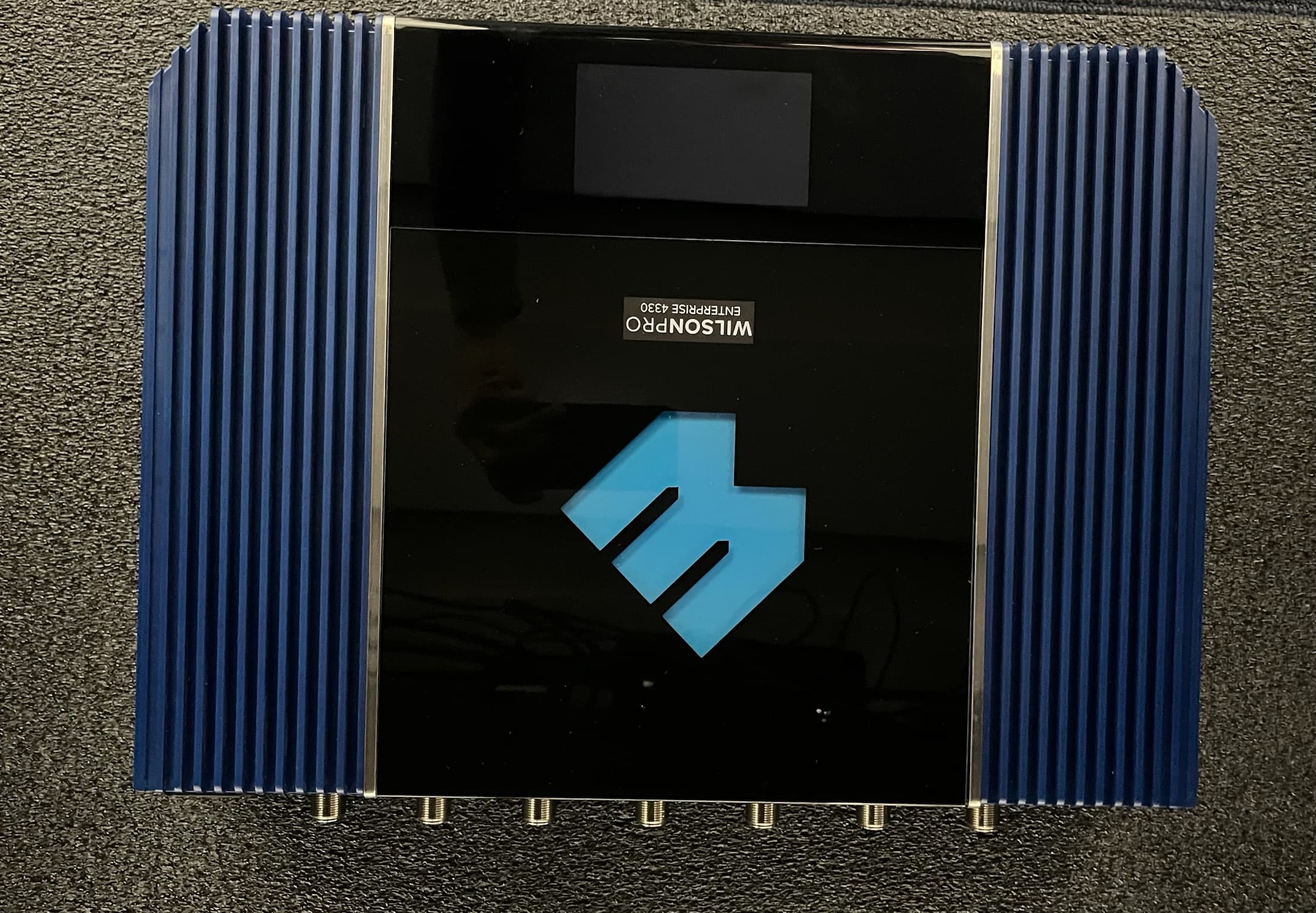
PWO075
Jan 10, 2024Quint Band Signal Booster
Equipment Class
B2W - Part 20 Wideband Consumer Booster (CMRS)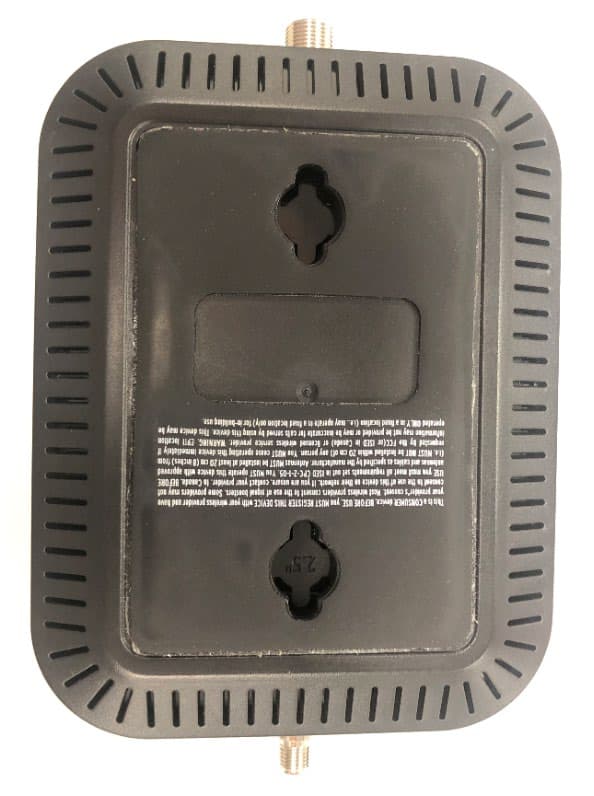
PWO460065
Nov 04, 2020Dual Band Signal Booster
Equipment Class
B2W - Part 20 Wideband Consumer Booster (CMRS)
PWO460061
Sep 22, 2020Quint Band Signal Booster
Equipment Class
B2W - Part 20 Wideband Consumer Booster (CMRS)