Q6MZBUPH0001ZigBee Module
ICP DAS Co., Ltd.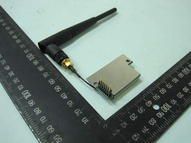
Click to zoom
Application Details
- Equipment Class
- DTS - Digital Transmission System
- Date of Grant
- May 16, 2010
- Application Purpose
- Original Equipment
- Date of Application
- May 16, 2010
- Equipment Note
- ZigBee Module
- Frequency Range
- 2405.00000000 - 2475.00000000
- Company
- ICP DAS Co., Ltd.
- Country
- Taiwan
Documents & Files
Document Text
Text extracted from the exhibit documents filed with the FCC. Open a document above to read the original.
Users Manual
Product #:ZB-UPH01 Confidential Page 1/14 Doc. #: ZB-UPH01 Reference Note <Rev. 0.9> ZB-UPH01 ZigBee Transceiver Module User Manual Version 0.9 Product #:ZB-UPH01 Confidential Page 2/14 Doc. #: ZB-UPH01 Reference Note <Rev. 0.9> TABLE OF CONTENTS 1 GENERAL INFORMATION... ..............................................3 2 POWER SAVING MODES ...................................................4 3 CONNECTORS PIN CONFIGURATION ... .............................5 4 ELECTRICAL SPECIFICATIONS .........................................6 5 DESIGN GUIDE TO AVOID RF INTERFERENCE ....................7 6 RF PERFORMANCE TEST DATA .........................................10 7 REFERENCE REFLOW TEMPETURE CURVE.......................11 8 REFERENCE DOCUMENTS.................................................11 Product #:ZB-UPH01 Confidential Page 3/14 Doc. #: ZB-UPH01 Reference Note <Rev. 0.9> Revised Date: Apr.14, 2010 1. GENERAL INFORMATION The ZB-UPH01 is a miniature 2.4 GHz Direct Sequence Spread Spectrum 802.15.4 transceiver. It includes all RF hardware and a micro-controller to manage the communications link. The micro-controller manages all communications task including configuration, data packaging, and clear channel selection. The result is a complete wireless data communications solution. The ZB-UPH01 package is unique because of its small form factor (32 x 23 mm 2 ), It has an on-board chip antenna and the availability of external dipole antenna I-PEX connector. No competitive products can offer a solution as flexible, convenient, and easy to integrate. Models • ZB-UPH01: Same as ZB-UPH01 but adding external SRAM Features • 32 x 23 mm 2 PCBA package with 2 connectors • Utilizes globally available 2.4 GHz ISM band • Programmable Transmit Power Output, max. 9dBm. • Complete IEEE 802.15.4 Spec. compliant. • Typical Receiver Sensitivity –101dBm. • Typical Data Rate 250Kbps. • Multiple Low Power Operating modes • Meet RoHS Requirement Product #:ZB-UPH01 Confidential Page 4/14 Doc. #: ZB-UPH01 Reference Note <Rev. 0.9> 2. POWER SAVING MODES The ZB-UPH01 includes several low power operating modes to permit the most efficient use of the available power. Below are descriptions of the available selections. ACTIVE: In Active Mode, all ZB-UPH01 circuits are powered and available for immediate action. This includes the RF receiver which actively monitors the air for an incoming communications request. Two sub-modes are classified as TX-ACTIVE and RX-ACTIVE. The current consumption of TX-ACTIVE is 44 mA while RX-ACTIVE is 38 mA. Product #:ZB-UPH01 Confidential Page 5/14 Doc. #: ZB-UPH01 Reference Note <Rev. 0.9> 3. CONNECTORS PIN CONFIGURATION ZB-UPH01 uses Silicon-Lab C8051F340 as MCU. It is an 8051 base MCU and reserves 10 GPIO pins for external controlling by application. Each pin can be a general I/O pin and programmed it by user directly. Furthermore, most of these pins can be used as special purpose function. Thereof TX, RX pins can be programmed as UART for data communication. For example, user is easy to connect these pins with RS485 transceivers such as 75176, MAX485. J1 Pin Configuration Signal Pin Description C2CK 1 Clock signal for the C2 Debug Interface. C2D 2 Bi-directional data signal for the C2 Debug Interface. VCC 3 3.3 Volt power for the ZB-UPH01 TX 4 GPIO, also used as UART TX. GND 5 Ground RX 6 GPIO, also used as UART RX. GPIO1 7 Bidirectional input/output Pin. It also can be programmed as analog to digital converter (ADC1) GPIO2 8 Bidirectional input/output Pin. It also can be programmed as analog to digital converter (ADC2) J2 Pin Configuration Signal Pin Description GPIO3 1 Bidirectional input/output Pin. It also can be programmed as analog to digital converter (ADC3) GPIO4 2 Bidirectional input/output Pin. It also can be programmed as analog to digital converter (ADC4) GPIO5 3 Bidirectional input/output Pin. GPIO6 4 Bidirectional input/output Pin. It also can be programmed as analog to digital converter (ADC5) GPIO7 5 Bidirectional input/output Pin. It also can be programmed as analog to digital converter (ADC6) GPIO8 6 Bidirectional input/output Pin. Product #:ZB-UPH01 Confidential Page 6/14 Doc. #: ZB-UPH01 Reference Note <Rev. 0.9> 4. ELECTRICAL SPECIFICATIONS Absolute Maximum Rating VCC 3.6V Storage temperature -40°C to +120°C Operating temperature Range -30°C to +80°C WARNING: Exceeding any of these ratings will void the warranty and may damage the device Parameters Min Typ Max Units Supply Voltage for RF, analog and digital circuits3 3.3 3.6 V Digital I/O Pin Input High Voltage 2.0 V Digital I/O Pin Input Low Voltage 0.8 V Analog Input Pin Input Voltage 0 3.3 V I/O Pin Output High Current 4 8 mA I/O Pin Output Low Current 8 14 mA I/O Pin Input High Current 0 10 uA I/O Pin Input Low Current 0 10 uA Current Consumption ACTIVE TX Mode @ 9 dBm 44 mA ACTIVE RX Mode 38 mA Output Power 9 dBm Wireless Receive Sensitivity -101 dBm Selectable Channels 16 channel Frequency Band 2.400 2.835 GHz Antenna Output Impedance 50 Ohms Product #:ZB-UPH01 Confidential Page 7/14 Doc. #: ZB-UPH01 Reference Note <Rev. 0.9> 5. DESIGN GUIDE TO AVOID RF INTERFERENCE When RF module put on an application board(mother board), to minimize the RF signal interference, the best way is to define an isolation area. This area should have no any trace or grounding pad. Here are some layout suggestions for mother board. Suggestion 1: Place RF board aside mother board. (Let antenna part outside mother board is better) Make sure no trace and grounding pad under the must isolate area. Please see the drawing as below. Mother Board Module Board Must Isolate Area Antenna Prefer Isolate Area Via Suggestion 2: Place RF board at the corner of mother board. Make sure no trace and grounding pad under the must isolate area. Please see the drawing as below. Customer's Mother Board RF Module Board Must Isolate Area Antenna Prefer Isolate Area Via Product #:ZB-UPH01 Confidential Page 8/14 Doc. #: ZB-UPH01 Reference Note <Rev. 0.9> Suggesti…
Text truncated - open the document above for the full version.
Cover Letter(s)
Page No. : 21 Limited Module Approval Request Letter Subject: Limited Module Approval Date: 2010/4/16 FCC ID: Q6MZBUPH0001 Dear Reviewer, We, Sporton International Inc., are authorized by ICP DAS CO., LTD. to have their state-of-the-art ZigBee Module approved under limited module approval authorization. The application of this module is specified to mobile host equipment. The requirements regulated in Public Notice DA00-1407 have been fulfilled and clearly explained below. 1. The requirement of RF shielding: The shielding of the radio portion can be demonstrated in exhibition External Photo. 2. The requirement of buffered inputs: Buffered data inputs stage has been integrated in chip C8051F340. 3. The requirement of power supply regulation: No power regulator can provide stability power source. But specific of hosts have 3.3Vdc regulator to provide stability power via mini-PCI interface to EUT. 4. The requirements of section 15.203 and 15.204(C): The requirements of antenna connector and spurious emission have been fulfilled. Please reference the exhibition Test Report. 5. The requirement of stand-alone test configuration: Please reference exhibition Test Configuration Photo for the stand-alone test configuration. 6. The requirement of labeling: The instruction on the labeling rule of the end product has been stated in the users manual of this module. Please also see the exhibition Label Sample. 7. The requirement of compliance on specific rule or operating requirements: The required FCC rule has been fulfilled and all the instructions for maintaining compliance has been clearly stated in the Users Manual. 8. The requirement of RF exposure: N/A as exempted due to low output power. Please do not hesitate to contact me for any questions of this request letter. Thank you. Company name : Sporton International Inc. Company Address : No.8, Lane 724, Bo-ai St., Jhubei City, Hsinchu County 302, Taiwan, R.O.C. Signature : Name : Leo Huang Job Title : Manager
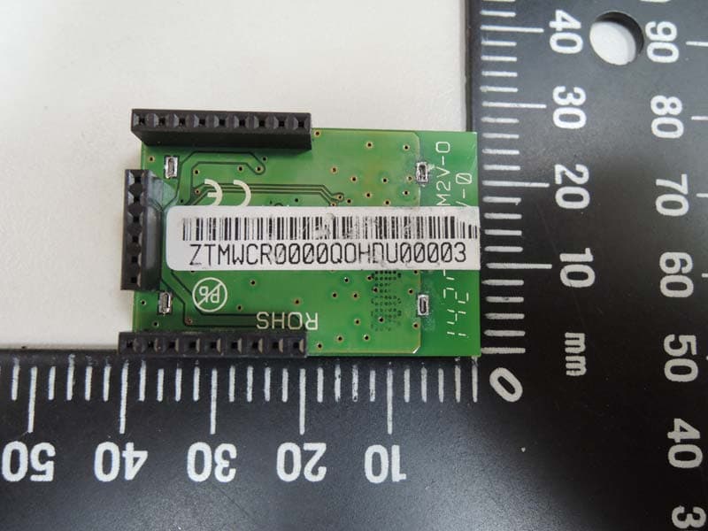
External Photos
SPORTON International Inc. PAGE NUMBER : A1 OF A4 TEL : 886-2-2696-2468 ISSUED DATE : May 06, 2010 FAX : 886-2-2696-2255 APPENDIX A. Photographs of EUT SPORTON International Inc. PAGE NUMBER : A2 OF A4 TEL : 886-2-2696-2468 ISSUED DATE : May 06, 2010 FAX : 886-2-2696-2255 SPORTON International Inc. PAGE NUMBER : A3 OF A4 TEL : 886-2-2696-2468 ISSUED DATE : May 06, 2010 FAX : 886-2-2696-2255 SPORTON International Inc. PAGE NUMBER : A4 OF A4 TEL : 886-2-2696-2468 ISSUED DATE : May 06, 2010 FAX : 886-2-2696-2255
Internal Photos
SPORTON International Inc. PAGE NUMBER : A1 OF A5 TEL : 886-2-2696-2468 ISSUED DATE : May 06, 2010 FAX : 886-2-2696-2255 APPENDIX A. Photographs of EUT SPORTON International Inc. PAGE NUMBER : A2 OF A5 TEL : 886-2-2696-2468 ISSUED DATE : May 06, 2010 FAX : 886-2-2696-2255 SPORTON International Inc. PAGE NUMBER : A3 OF A5 TEL : 886-2-2696-2468 ISSUED DATE : May 06, 2010 FAX : 886-2-2696-2255 SPORTON International Inc. PAGE NUMBER : A4 OF A5 TEL : 886-2-2696-2468 ISSUED DATE : May 06, 2010 FAX : 886-2-2696-2255 SPORTON International Inc. PAGE NUMBER : A5 OF A5 TEL : 886-2-2696-2468 ISSUED DATE : May 06, 2010 FAX : 886-2-2696-2255
Test Report
SPORTON International Inc. No. 52, Hwa Ya 1st Rd., Kwei-Shan Hsiang, TaoYuan Hsien, Taiwan, R.O.C. Ph: 886-3-327-3456 / FAX: 886-3-327-0973 / www.sporton.com.tw Report Format Version: 01 FCC RADIO TEST REPORT Applicant’s company ICP DAS CO., LTD. Applicant Address No. 111, Kuangfu N. Rd., Hukon Shiang, Hsinchu, Taiwan 303, R.O.C. FCC ID Q6MZBUPH0001 Manufacturer’s company ICP DAS CO., LTD. Manufacturer Address No. 111, Kuangfu N. Rd., Hukon Shiang, Hsinchu, Taiwan 303, R.O.C. Product Name ZigBee Module Brand Name ICP DAS Model Name ZB-UPH01 Test Rule 47 CFR FCC Part 15 Subpart C § 15.247 Test Freq. Range 2405 ~ 2475MHz Received Date Apr. 02, 2010 Final Test Date May 06, 2010 Submission Type Original Equipment Statement Test result included is only for the IEEE 802.15.4 ZigBee part of the product. The test result in this report refers exclusively to the presented test model / sample. Without written approval of SPORTON International Inc., the test report shall not be reproduced except in full. The measurements and test results shown in this test report were made in accordance with the procedures and found in compliance with the limit given in ANSI C63.4-2003 and 47 CFR FCC Part 15 Subpart C. The test equipment used to perform the test is calibrated and traceable to NML/ROC. Report No.: FR040225 Report Format Version: 01 Page No. : i of ii FCC ID: Q6MZBUPH0001 Issued Date : May 06, 2010 Table of Contents 1. CERTIFICATE OF COMPLIANCE ......................................................................................................................... 1 2. SUMMARY OF THE TEST RESULT .......................................................................................................................... 2 3. GENERAL INFORMATION .................................................................................................................................. 3 3.1. Product Details....................................................................................................................................................................................3 3.2. Accessories .........................................................................................................................................................................................3 3.3. Table for Filed Antenna.......................................................................................................................................................................3 3.4. Table for Carrier Frequencies .............................................................................................................................................................3 3.5. Table for Test Modes ...........................................................................................................................................................................4 3.6. Table for Testing Locations..................................................................................................................................................................4 3.7. Table for Supporting Units ...................................................................................................................................................................5 3.8. Table for Parameters of Test Software Setting .....................................................................................................................................5 3.9. Test Configurations .............................................................................................................................................................................6 4. TEST RESULT ..................................................................................................................................................... 8 4.1. AC Power Line Conducted Emissions Measurement...........................................................................................................................8 4.2. Maximum Conducted Output Power Measurement .........................................................................................................................12 4.3. Power Spectral Density Measurement ..............................................................................................................................................16 4.4. 6dB Spectrum Bandwidth Measurement ..........................................................................................................................................20 4.5. Radiated Emissions Measurement ....................................................................................................................................................24 4.6. Band Edge Emissions Measurement .................................................................................................................................................33 4.7. Antenna Requirements .....................................................................................................................................................................36 5. LIST OF MEASURING EQUIPMENTS ................................................................................................................... 37 TEST LOCATION ................................................................................................................................................. 39 6. TAF CERTIFICATE OF ACCREDITATION ............................................................................................................. 40 APPENDIX A. PHOTOGRAPHS OF EUT.......................................................................................................... A1 ~ A8 APPENDIX B. TEST PHOTOS.......................................................................................................................... B1 ~ B6 Report No.: FR040225 Report Format Version: 01 Page No. : ii of ii FCC ID: Q6MZBUPH0001 Issued Date : May 06, 2010 History of T…
Text truncated - open the document above for the full version.
Test Setup Photos
Report No.: FR040225 FCC ID: Q6MZBUPH0001 Page No. : 1 of 6 Appendix B. Test Photos Report No.: FR040225 FCC ID: Q6MZBUPH0001 Page No. : 2 of 6 1. Photographs of Conducted Emissions Test Configuration FRONT VIEW REAR VIEW Report No.: FR040225 FCC ID: Q6MZBUPH0001 Page No. : 3 of 6 2. Photographs of Radiated Emissions Test Configuration Test Configuration: 9kHz ~30MHz FRONT VIEW REAR VIEW Report No.: FR040225 FCC ID: Q6MZBUPH0001 Page No. : 4 of 6 Test Configuration: 30MHz~1GHz FRONT VIEW REAR VIEW Report No.: FR040225 FCC ID: Q6MZBUPH0001 Page No. : 5 of 6 SIDE VIEW Report No.: FR040225 FCC ID: Q6MZBUPH0001 Page No. : 6 of 6 Test Configuration: Above 1GHz FRONT VIEW REAR VIEW
Contact Information
Applicant
King Fu(Engineer)
Test Firm
Sporton International Inc.Alex Chen
Technical Specifications
| # | Rule Parts | Frequency Range | Power Output |
|---|---|---|---|
| 1 | 15C | 2.40 GHz - 2.48 GHz | 5.80 mW |
Other Applications from ICP DAS Co., Ltd.
Q6M-ZTM-WP
Jul 15, 2015RF Modem
Equipment Class
DTS - Digital Transmission System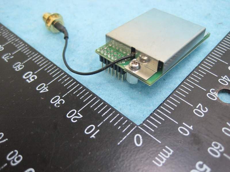
Q6M-ZM31001100-PA
Mar 17, 2013Wireless Module
Equipment Class
DTS - Digital Transmission System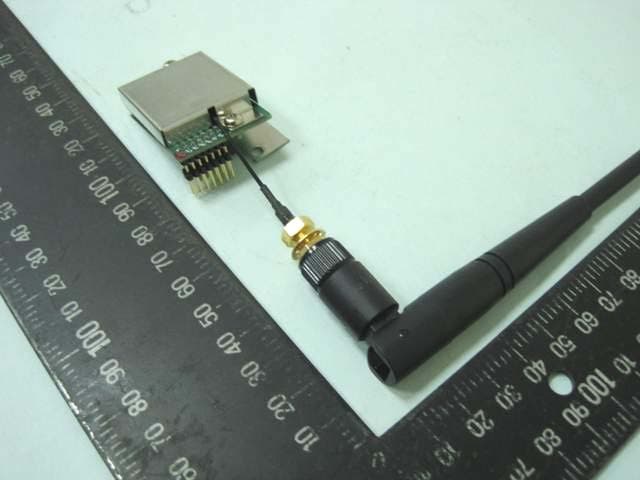
Q6MZBUPS0001
May 16, 2010ZigBee Module
Equipment Class
DTS - Digital Transmission System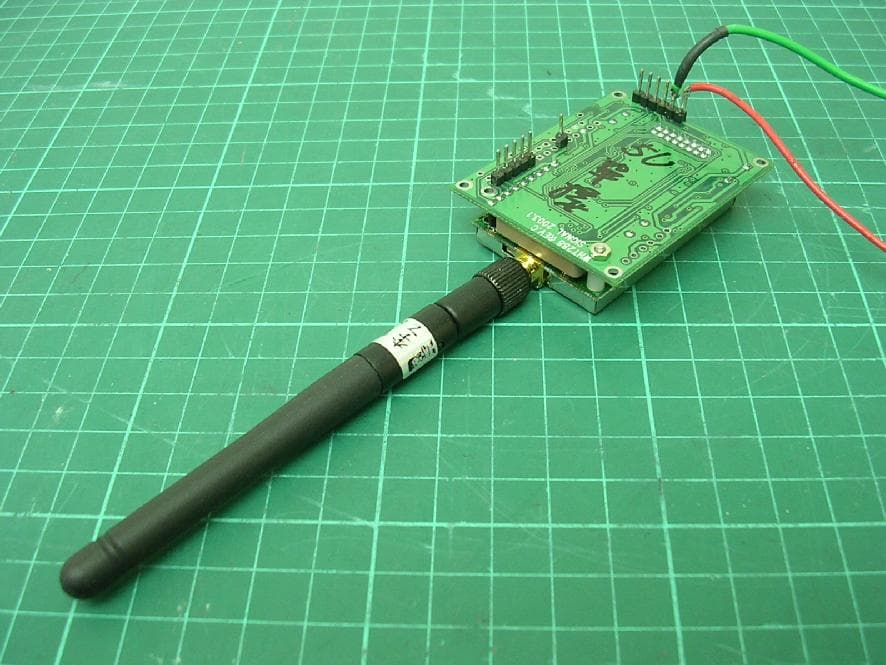
Q6M3SDSST-24M
Mar 31, 2005Wireless Modem Module
Equipment Class
DTS - Digital Transmission System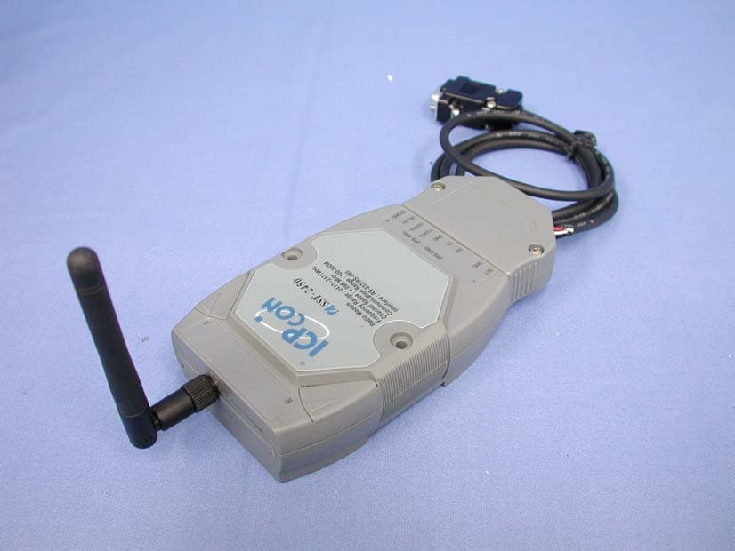
Q6MIT450000
Jun 02, 2003Wireless Modem
Equipment Class
DTS - Digital Transmission System