R8KUGWC821RNEMO BLUETOOTH RADIO MODULE
Unigen Corporation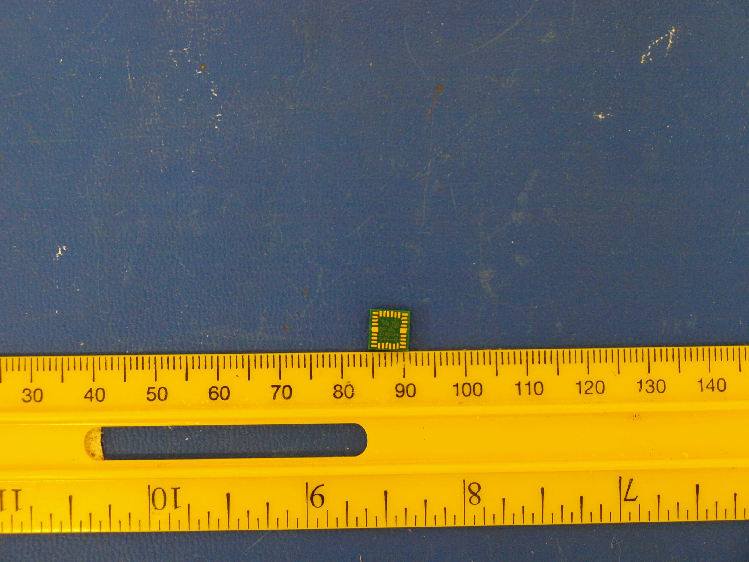
Click to zoom
Application Details
- Equipment Class
- DSS - Part 15 Spread Spectrum Transmitter
- Date of Grant
- Jun 14, 2012
- Application Purpose
- Original Equipment
- Date of Application
- Jun 12, 2012
- Equipment Note
- NEMO BLUETOOTH RADIO MODULE
- Frequency Range
- 2402.00000000 - 2480.00000000
- Company
- Unigen Corporation
- Country
- United States
Documents & Files
Document Text
Text extracted from the exhibit documents filed with the FCC. Open a document above to read the original.
Users Manual
NEMO Bluetooth Radio Module Solutions for a Real Time World Datasheet Re-Tek - 1573 - 1 - 45388 Warm Springs Blvd. Fremont, CA 94539 [email protected] TEL: (510) 668.2088 FAX: (510) 661.2788 http://www.unigen.com Customer Comment Line: (800) 826.0808 Copyright Unigen Corporation, 2008 Unigen Corp. Wireless Module Products NEMO Bluetooth Radio Modules UGWC621RSMA133 Issue Date: 18-Aug-09 Revision: 1.1 NEMO Bluetooth Radio Module Solutions for a Real Time World Datasheet Re-Tek - 1573 - 2 - 45388 Warm Springs Blvd. Fremont, CA 94539 [email protected] TEL: (510) 668.2088 FAX: (510) 661.2788 http://www.unigen.com Customer Comment Line: (800) 826.0808 Copyright Unigen Corporation, 2008 Revision History Rev. No. History Issue DateRemarks 1.0 Draft Dec. 5, 2008 Advanced information; Author: Allen B. Cabreros 1.1 Revision Aug. 18, 2009 Added dimensional drawings. THIS DOCUMENT IS PROVIDED “AS IS” WITH NO WARRANTIES WHATSOEVER, INCLUDING ANY WARRANTY OF MERCHANTABILITY, NON-INFRINGEMENT, FITNESS FOR ANY PARTICULAR PURPOSE, OR ANY WARRANTY OTHERWISE ARISING OUT OF ANY PROPOSAL, SPECIFICATION OR SAMPLE. Unigen Corporation disclaims all liability, including liability for infringement of any proprietary rights, relating to use of information in this document. No license, expressed or implied, by estoppel or otherwise, to any intellectual property rights is granted herein. *Third-party brands, names, and trademarks are the property of their respective owners. NEMO Bluetooth Radio Module Solutions for a Real Time World Datasheet Re-Tek - 1573 - 3 - 45388 Warm Springs Blvd. Fremont, CA 94539 [email protected] TEL: (510) 668.2088 FAX: (510) 661.2788 http://www.unigen.com Customer Comment Line: (800) 826.0808 Copyright Unigen Corporation, 2008 TABLE OF CONTENTS LIST OF FIGURES __________________________________________ 4 LIST OF TABLES ___________________________________________ 5 PRODUCT INTRODUCTION ___________________________________ 6 PRODUCT INTRODUCTION ___________________________________ 6 FEATURES AND BENEFITS____________________________________ 6 PRODUCT DESCRIPTION_____________________________________ 8 NEMO Module __________________________________________ 8 CSR BlueCore 6 ROM Transceiver IC _________________________ 8 Functional Block Diagrams ________________________________ 9 PIN ASSIGNMENT __________________________________________ 11 PIN FUNCTIONS ___________________________________________ 12 ABSOLUTE MAXIMUM RATINGS _______________________________ 13 RECOMMENDED OPERATING CONDITIONS ______________________ 13 RF CHARACTERISTICS ______________________________________ 14 EXTERNAL SLOW CLOCK SOURCE CHARACTERISTICS ______________ 14 AGENCY CERTIFICATIONS (PRE-SCAN) _________________________ 15 REGULATORY COMPLIANCE STATEMENT ________________________ 15 FUNCTIONAL OVERVIEW ____________________________________ 16 NEMO Hardware Functional Description ______________________ 16 NEMO Firmware Functional Description ______________________ 17 CSR BLUETOOTH SOFTWARE STACK ____________________________ 18 Key Features of the HCI Stack: Standard Bluetooth Functionality __ 19 Key Features of the HCI Stack: Extra Functionality______________ 21 DIGITAL INTERFACES _______________________________________ 22 High Speed UART Interface________________________________ 22 BlueCore Serial Protocol (BCSP) ____________________________ 22 BLUECORE COMMAND (BCCMD) PROTOCOL ______________________ 24 Audio PCM and I2S Interfaces _____________________________ 25 PCM Interface Master/Slave _______________________________ 25 PCM Long Frame Sync ____________________________________ 27 Short Frame Sync _______________________________________ 28 Multi-slot Operation _____________________________________ 29 GCI Interface __________________________________________ 30 PCM Slots and Sample Formats _____________________________ 31 PCM Timing Information __________________________________ 32 PCM CLK and PCM SYNC Generation _________________________ 34 PCM Configuration ______________________________________ 35 Digital Audio Interface (I²S) _______________________________ 38 Figure 20: Digital Audio Interface Master Timing _______________ 41 POWER CONSUMPTION _____________________________________ 42 BOOTING NEMO ROM _______________________________________ 44 NEMO Bluetooth Radio Module Solutions for a Real Time World Datasheet Re-Tek - 1573 - 4 - 45388 Warm Springs Blvd. Fremont, CA 94539 [email protected] TEL: (510) 668.2088 FAX: (510) 661.2788 http://www.unigen.com Customer Comment Line: (800) 826.0808 Copyright Unigen Corporation, 2008 UART Auto Baud Rate ____________________________________ 44 Persistent Store Keys (PSKEYS) ____________________________ 45 TYPICAL APPLICATION CIRCUITS _____________________________ 48 NEMO with out external 32kHz slow clock source: ______________ 48 NEMO with external 32kHz slow clock source: _________________ 49 MECHANICAL DRAWINGS ____________________________________ 50 REFERENCE DOCUMENTATION ________________________________ 51 CONTACT INFORMATION ____________________________________ 51 LIST OF FIGURES Figure 1: NEMO Module Block Diagram__________________________ 9 Figure 2: CSR BlueCore 6 ROM Block Diagram ____________________ 10 Figure 3: NEMO Module Pin Locations __________________________ 11 Figure 4: BlueCore Bluetooth HCI Stack _________________________ 18 Figure 5: UART Host Connection _______________________________ 23 Figure 6: BCSP Context ______________________________________ 23 Figure 7: BCCMD Interface ___________________________________ 24 Figure 8: PCM Interface Master _______________________________ 25 Figure 9: PCM Interface Slave_________________________________ 26 Figure 10: Long Frame Sync (Shown with 8-bit Companded Sample) __ 27 Figure 11: Short Frame Sync (Shown with 16-bit Sample) ___________ 28 Figure 12: Multi-slot Operation with Two Slots and 8-bit Companded Samples ________________________________________________________ 29 Figure 13: GCI Interface ______________…
Text truncated - open the document above for the full version.
Users Manual
Solutions for a Real Time World NEMO2 Design Guidelines Application note Unigen Corp. Wireless Module Products NEMO Bluetooth Radio Modules UGWC821RSMA133 Design Guidelines Application Note Issue Date: April 3 rd , 2012 Revision: 1.0 Solutions for a Real Time World NEMO2 Design Guidelines Application note CONTENTS Contents ........................................................................................................................................................ 2 List of Figures ................................................................................................................................................ 4 List of Tables ................................................................................................................................................. 5 Scope ............................................................................................................................................................. 6 FCC Transmitter Modular Approval Introduction ......................................................................................... 6 Class 2 Permissive Changes ........................................................................................................................... 7 NEMO2 Module General Description ........................................................................................................... 7 CSR BlueCore 6 ROM Transceiver IC ............................................................................................................. 8 Functional Block Diagrams ............................................................................................................................ 9 Nemo2 LGA Form Factor ............................................................................................................................. 12 LGA Pads and Assignments ..................................................................................................................... 12 Nemo2 Reference Evaluation Board ........................................................................................................... 14 Nemo2 Evaluation Board BOM ............................................................................................................... 16 PCB Layout .............................................................................................................................................. 17 Component Layout.................................................................................................................................. 17 Top Layer (Layer 1) .................................................................................................................................. 18 Ground Layer (Layer 2) ........................................................................................................................... 18 VDD Layer (Layer 3) ................................................................................................................................. 19 Bottom Layer (Layer 4) ............................................................................................................................ 20 PCB Stack, Materials, Drill & Notes ......................................................................................................... 21 NEMO 2 Design Integration Rules ............................................................................................................... 22 Intended Use ........................................................................................................................................... 22 Solutions for a Real Time World NEMO2 Design Guidelines Application note Antenna & External RF Path .................................................................................................................... 24 Microstrip Transmission Line Specification ............................................................................................ 25 Microstrip PCB Board Details: ................................................................................................................. 26 Microstrip Ground Reference ................................................................................................................. 26 RF Shielding ............................................................................................................................................. 29 Support Contact ...................................................................................................................................... 31 Solutions for a Real Time World NEMO2 Design Guidelines Application note LIST OF FIGURES Figure 1: Nemo2 Basic Block Diagram .......................................................................................................... 9 Figure 2: CSR BlueCore 6 Chipset Block Diagram ........................................................................................ 10 Figure 3: NEMO2 Elaborate Block Diagram ................................................................................................ 11 Figure 4: NEMO2 LGA Pads ......................................................................................................................... 12 Figure 5: NEMO2 Evaluation board ............................................................................................................ 14 Figure 6: NEMO2 Evaluation Board Component Layout ............................................................................. 17 Figure 7: NEMO2 Evaluation Board Top Layer 1 ......................................................................................... 18 Figure 8: NEMO2 Evaluation Board Ground Layer 2 ................................................................................... 18 Figure 9: NEMO2 Power Plane Layer 3 ....................................................................................................... 19 Figure 10: NEMO2 Bottom Signal …
Text truncated - open the document above for the full version.
Cover Letter(s)
Applicant/Grantee UNIGEN CORPORATION FCC ID: R8KUGWC821R Section 15.212 Modular Transmitters Request for Modular Approval Request for Limited Modular Approval Requirements EUT Conditions Comply (Y/N) Single Modular Approval Requirements 1 The radio elements of the modular transmitter must have their own shielding. The physical crystal and tuning capacitors may be located external to the shielded radio elements. No. The OEM is required to install the shield during manufacturing per the detailed instructions in the OEM installation guidelines that is available to OEMs. N 2 The modular transmitter must have buffered modulation/data inputs (if such inputs are provided) to ensure that the module will comply with Part 15 requirements under conditions of excessive data rates or over-modulation. Y 3 The modular transmitter must have its own power supply regulation. Y 4 The modular transmitter must comply with the antenna and transmission system requirements of Sections 15.203, 15.204(b) and 15.204(c). The antenna must either be permanently attached or employ a “unique” antenna coupler (at all connections between the module and the antenna, including the cable). The “professional installation” provision of Section 15.203 is not applicable to modules but can apply to limited modular approvals under paragraph (b) of this section. No. The OEM is required to install an antenna and antenna trace following the detailed OEM installation guide lines provided and available to OEMs. N 5 The modular transmitter must be tested in a stand-alone configuration, i.e., the module must not be inside another device during testing for compliance with Part 15 requirements. Unless the transmitter module will be battery powered, it must comply with the AC line conducted requirements found in Section 15.207. AC or DC power lines and data input/output lines connected to the module must not contain ferrites, unless they will be marketed with the module (see Section 15.27(a)). The length of these lines shall be the length typical of actual use or, if that length is unknown, at least 10 centimeters to insure that there is no coupling between the case of the module and supporting Y equipment. Any accessories, peripherals, or support equipment connected to the module during testing shall be unmodified and commercially available (see Section 15.31(i)). 6 The modular transmitter must be equipped with either a permanently affixed label or must be capable of electronically displaying its FCC identification number. (A) If using a permanently affixed label, the modular transmitter must be labeled with its own FCC identification number, and, if the FCC identification number is not visible when the module is installed inside another device, then the outside of the device into which the module is installed must also display a label referring to the enclosed module. This exterior label can use wording such as the following: “Contains Transmitter Module FCC ID: XYZMODEL1” or “Contains FCC ID: XYZMODEL1.” Any similar wording that expresses the same meaning may be used. The Grantee may either provide such a label, an example of which must be included in the application for equipment authorization, or, must provide adequate instructions along with the module which explain this requirement. In the latter case, a copy of these instructions must be included in the application for equipment authorization. (B) If the modular transmitter uses an electronic display of the FCC identification number, the information must be readily accessible and visible on the modular transmitter or on the device in which it is installed. If the module is installed inside another device, then the outside of the device into which the module is installed must display a label referring to the enclosed module. This exterior label can use wording such as the following: “Contains FCC certified transmitter module(s).” Any similar wording that expresses the same meaning may be used. The user manual must include instructions on how to access the electronic display. A copy of these instructions must be included in the application for equipment authorization. Device is too small to accommodate the FCC ID and two-part statement. See EUT photograph of the device. The device is a module and the customer intended to include the FCC ID and statement in the OEM\Installer instructions. Per KDB 411029, FCC informed TCB should file a PBA at time of fling the application in order to receive further guidance on your certified. See uploaded KDB 411029. N 7 The modular transmitter must comply with any specific rules or operating requirements that ordinarily apply to a complete transmitter and the manufacturer must provide adequate instructions along with the module to explain any such requirements. A copy of these instructions must be included in the application for equipment authorization. Y 8 The modular transmitter must comply with any applicable RF exposure requirements in its final configuration. Y A limited modular approval may be granted for single or split modular transmitters that do not comply with all of the above requirements, e.g., shielding, minimum signaling amplitude, buffered modulation/data inputs, or power supply regulation, if the manufacturer can demonstrate by alternative means in the application for equipment authorization that the modular transmitter meets all the applicable Part 15 requirements under the operating conditions in which the transmitter will be used. Limited modular approval also may be granted in those instances where compliance with RF exposure rules is demonstrated only for particular product configurations. The applicant for certification must state how control of the end product into which the module will be installed will be maintained such that full compliance of the end product is always ensured.
ID Label/Location Info
Inquiry: A pre‐TCB KDB inquiry was submitted to FCC under to request guidance on the fact that the module is apparently too small to include the FCC ID label and information and does not support electronic labeling; therefore the grantee provides the FCC ID in the OEM installation guidance documentation along with instructions to label the host with the FCC ID. The FCC responded that a PBA should be submitted by the TCB. It is not clear to the TCB if the FCC response allows this approach or required electronic labeling as the only alternative to no physical label on the module. FCC response on 06/14/2012 At that time the FCC did require TCBs to request PBAs for certain label issues. With the given size of the module, the FCC approves the PBA for the device in question.
Test Report
FCC CFR47 PART 15 SUBPART C INDUSTRY CANADA RSS-210 ISSUE 8 CERTIFICATION TEST REPORT FOR NEMO BLUETOOTH RADIO MODULE MODEL NUMBER: UGWC821RSMA133 FCC ID: R8KUGWC821R IC: 5125A-UGWC821R REPORT NUMBER: 11U13608-1 ISSUE DATE: MAY 04, 2011 Prepared for Unigen Corporation 45388 Warm Springs Blvd. Fremont, CA, 94538 U.S.A. Prepared by COMPLIANCE CERTIFICATION SERVICES (UL CCS) 47173 BENICIA STREET FREMONT, CA 94538, U.S.A. TEL: (510) 771-1000 FAX: (510) 661-0888 REPORT NO: 11U13608-1 DATE: MAY 04, 2011 FCC ID: R8KUGWC821R IC: 5125A-UGWC821R Page 2 of 98 COMPLIANCE CERTIFICATION SERVICES (UL CCS) FORM NO: CCSUP4701D 47173 BENICIA STREET, FREMONT, CA 94538, USA TEL: (510) 771-1000 FAX: (510) 661-0888 This report shall not be reproduced except in full, without the written approval of UL CCS. Revision History Rev. Issue Date Revisions Revised By -- 05/04/11 Initial Issue F. Ibrahim REPORT NO: 11U13608-1 DATE: MAY 04, 2011 FCC ID: R8KUGWC821R IC: 5125A-UGWC821R Page 3 of 98 COMPLIANCE CERTIFICATION SERVICES (UL CCS) FORM NO: CCSUP4701D 47173 BENICIA STREET, FREMONT, CA 94538, USA TEL: (510) 771-1000 FAX: (510) 661-0888 This report shall not be reproduced except in full, without the written approval of UL CCS. TABLE OF CONTENTS 1. ATTESTATION OF TEST RESULTS .................................................................................... 5 2. TEST METHODOLOGY ........................................................................................................ 6 3. FACILITIES AND ACCREDITATION .................................................................................... 6 4. CALIBRATION AND UNCERTAINTY .................................................................................. 6 4.1. MEASURING INSTRUMENT CALIBRATION ................................................................ 6 4.2. SAMPLE CALCULATION ............................................................................................... 6 4.3. MEASUREMENT UNCERTAINTY ................................................................................. 6 5. EQUIPMENT UNDER TEST ................................................................................................. 7 5.1. DESCRIPTION OF EUT ................................................................................................. 7 5.2. MAXIMUM OUTPUT POWER ........................................................................................ 7 5.3. DESCRIPTION OF AVAILABLE ANTENNAS ................................................................ 7 5.1. SOFTWARE AND FIRMWARE ...................................................................................... 7 5.2. WORST-CASE CONFIGURATIONS AND MODE ......................................................... 8 5.3. DESCRIPTION OF TEST SETUP .................................................................................. 9 6. TEST AND MEASUREMENT EQUIPMENT ....................................................................... 11 7. ANTENNA PORT TEST RESULTS .................................................................................... 12 7.1. BASIC DATA RATE GFSK MODULATION .................................................................. 12 7.1.1. 20 dB AND 99% BANDWIDTH ............................................................................. 12 7.1.2. HOPPING FREQUENCY SEPARATION .............................................................. 17 7.1.3. NUMBER OF HOPPING CHANNELS ................................................................... 19 7.1.4. AVERAGE TIME OF OCCUPANCY ..................................................................... 22 7.1.5. OUTPUT POWER ................................................................................................. 26 7.1.6. AVERAGE POWER .............................................................................................. 29 7.1.7. CONDUCTED SPURIOUS EMISSIONS ............................................................... 30 7.2. ENHANCED DATA RATE 8PSK MODULATION ......................................................... 35 7.2.1. 20 dB AND 99% BANDWIDTH ............................................................................. 35 7.2.2. HOPPING FREQUENCY SEPARATION .............................................................. 40 7.2.3. NUMBER OF HOPPING CHANNELS ................................................................... 42 7.2.4. AVERAGE TIME OF OCCUPANCY ..................................................................... 45 7.2.5. OUTPUT POWER ................................................................................................. 49 7.2.6. AVERAGE POWER .............................................................................................. 52 7.2.7. CONDUCTED SPURIOUS EMISSIONS ............................................................... 53 7.3. DQPSK MODULATION ................................................................................................ 58 7.3.1. AVERAGE TIME OF OCCUPANCY ..................................................................... 58 7.3.2. OUTPUT POWER ................................................................................................. 64 7.3.3. AVERAGE POWER .............................................................................................. 67 8. RADIATED TEST RESULTS .............................................................................................. 68 REPORT NO: 11U13608-1 DATE: MAY 04, 2011 FCC ID: R8KUGWC821R IC: 5125A-UGWC821R Page 4 of 98 COMPLIANCE CERTIFICATION SERVICES (UL CCS) FORM NO: CCSUP4701D 47173 BENICIA STREET, FREMONT, CA 94538, USA TEL: (510) 771-1000 FAX: (510) 661-0888 This report shall not be reproduced except in full, without the written approval of UL CCS. 8.1. LIMITS AND PROCEDURE ......................................................................................... 68 8.2. TRANSMITTER ABOVE 1 GHz ................................................................................... 69 8.2.1. BASI…
Text truncated - open the document above for the full version.
Test Setup Photos
REPORT NO: 11U13608-1 DATE: MAY 04, 2011 FCC ID: R8KUGWC821R IC: 5125A-UGWC821R Page 92 of 98 COMPLIANCE CERTIFICATION SERVICES (UL CCS) FORM NO: CCSUP4701D 47173 BENICIA STREET, FREMONT, CA 94538, USA TEL: (510) 771-1000 FAX: (510) 661-0888 This report shall not be reproduced except in full, without the written approval of UL CCS. 11. SETUP PHOTOS ANTENNA PORT CONDUCTED RF MEASUREMENT SETUP ANTENNA PORT CONDUCTED PHOTO REPORT NO: 11U13608-1 DATE: MAY 04, 2011 FCC ID: R8KUGWC821R IC: 5125A-UGWC821R Page 93 of 98 COMPLIANCE CERTIFICATION SERVICES (UL CCS) FORM NO: CCSUP4701D 47173 BENICIA STREET, FREMONT, CA 94538, USA TEL: (510) 771-1000 FAX: (510) 661-0888 This report shall not be reproduced except in full, without the written approval of UL CCS. RADIATED RF MEASUREMENT SETUP FOR PORTABLE CONFIGURATION X-AXIS FRONT PHOTO REPORT NO: 11U13608-1 DATE: MAY 04, 2011 FCC ID: R8KUGWC821R IC: 5125A-UGWC821R Page 94 of 98 COMPLIANCE CERTIFICATION SERVICES (UL CCS) FORM NO: CCSUP4701D 47173 BENICIA STREET, FREMONT, CA 94538, USA TEL: (510) 771-1000 FAX: (510) 661-0888 This report shall not be reproduced except in full, without the written approval of UL CCS. X-AXIS BACK PHOTO REPORT NO: 11U13608-1 DATE: MAY 04, 2011 FCC ID: R8KUGWC821R IC: 5125A-UGWC821R Page 95 of 98 COMPLIANCE CERTIFICATION SERVICES (UL CCS) FORM NO: CCSUP4701D 47173 BENICIA STREET, FREMONT, CA 94538, USA TEL: (510) 771-1000 FAX: (510) 661-0888 This report shall not be reproduced except in full, without the written approval of UL CCS. Y-AXIS FRONT PHOTO REPORT NO: 11U13608-1 DATE: MAY 04, 2011 FCC ID: R8KUGWC821R IC: 5125A-UGWC821R Page 96 of 98 COMPLIANCE CERTIFICATION SERVICES (UL CCS) FORM NO: CCSUP4701D 47173 BENICIA STREET, FREMONT, CA 94538, USA TEL: (510) 771-1000 FAX: (510) 661-0888 This report shall not be reproduced except in full, without the written approval of UL CCS. Y-AXIS BACK PHOTO REPORT NO: 11U13608-1 DATE: MAY 04, 2011 FCC ID: R8KUGWC821R IC: 5125A-UGWC821R Page 97 of 98 COMPLIANCE CERTIFICATION SERVICES (UL CCS) FORM NO: CCSUP4701D 47173 BENICIA STREET, FREMONT, CA 94538, USA TEL: (510) 771-1000 FAX: (510) 661-0888 This report shall not be reproduced except in full, without the written approval of UL CCS. POWERLINE CONDUCTED EMISSIONS MEASUREMENT SETUP LINE CONDUCTED FRONT PHOTO REPORT NO: 11U13608-1 DATE: MAY 04, 2011 FCC ID: R8KUGWC821R IC: 5125A-UGWC821R Page 98 of 98 COMPLIANCE CERTIFICATION SERVICES (UL CCS) FORM NO: CCSUP4701D 47173 BENICIA STREET, FREMONT, CA 94538, USA TEL: (510) 771-1000 FAX: (510) 661-0888 This report shall not be reproduced except in full, without the written approval of UL CCS. END OF REPORT LINE CONDUCTED BACK PHOTO
Contact Information
Applicant
weerapol seesanung(Wireless Test Engineer)
Test Firm
Compliance Certification ServicesThu Chan
Technical Specifications
| # | Rule Parts | Frequency Range | Power Output |
|---|---|---|---|
| 1 | 15C | 2.40 GHz - 2.48 GHz | 9.60 mW |
Other Applications from Unigen Corporation
R8KUGWSX931
Nov 25, 2012900MHz Transceiver Module
Equipment Class
DTS - Digital Transmission System
R8KUGWT1BL1
Jan 26, 2012TETRA Dual Mode Bluetooth Radio Module
Equipment Class
DSS - Part 15 Spread Spectrum Transmitter
R8KUGWDS82
Jun 17, 2010802.11b/g/n WiFi Radio Module
Equipment Class
DTS - Digital Transmission System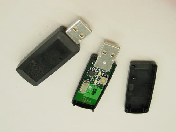
R8KUGQUBE1US
Dec 29, 2005USB Dongle
Equipment Class
DTS - Digital Transmission System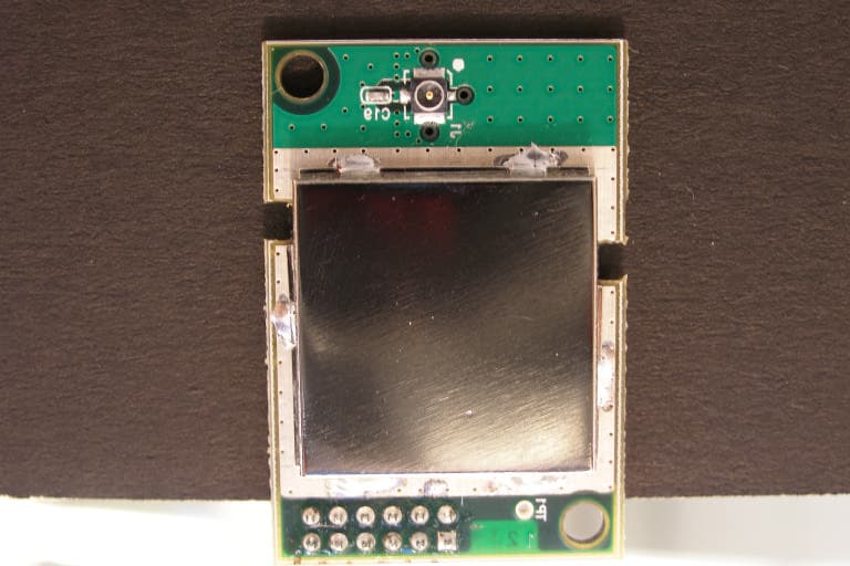
R8KUGWN2USHN33
Aug 24, 20052.4GHz Wireless Module
Equipment Class
DTS - Digital Transmission System