R8KUGWN2USHN332.4GHz Wireless Module
Unigen Corporation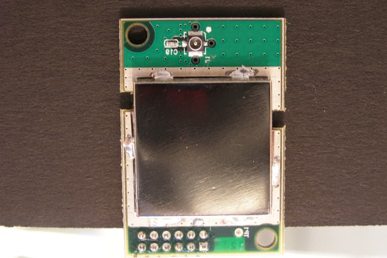
Click to zoom
Application Details
- Equipment Class
- DTS - Digital Transmission System
- Date of Grant
- Aug 24, 2005
- Application Purpose
- Original Equipment
- Date of Application
- Aug 24, 2005
- Equipment Note
- 2.4GHz Wireless Module
- Frequency Range
- 2402.00000000 - 2479.00000000
- Company
- Unigen Corporation
- Country
- United States
Documents & Files
Document Text
Text extracted from the exhibit documents filed with the FCC. Open a document above to read the original.
Users Manual
WirelessUSB™ - UGWN2US Solutions for a Real Time World User Manual UM-UGWN2US 1 45388 Warm Springs Blvd. Fremont, CA 94539 [email protected] TEL: (510) 668.2088 FAX: (510) 661.2788 http://www.unigen.com Toll Free: (800) 826.0808 Copyright Unigen Corporation, 2005 UNIGEN CORP. WIRELESS MODULE PRODUCTS P ART NUMBER FAMILY: UGWN2US SERIES JUNO-PAL WIRELESSUSB™ RADIO MODULE USER MANUAL FCC ID: R8KUGWN2USHN33 Issue Date: 30 July 2005 Revision: 0.95 Revision History Rev. No. History Issue Date Remarks 0.9 Draft Release 7 July, 2005 Pending FCC Grant # 0.95 2 nd Draft 30 July, 2005 Co-location of Antenna Updated due to 25mW and 20cm rules 1.0 Inclusion of FCC Grant THIS DOCUMENT IS PROVIDED “AS IS” WITH NO WARRANTIES WHATSOEVER, INCLUDING ANY WARRANTY OF MERCHANTABILITY, NON-INFRINGEMENT, FITNESS FOR ANY PARTICULAR PURPOSE, OR ANY WARRANTY OTHERWISE ARISING OUT OF ANY PROPOSAL, SPECIFICATION OR SAMPLE. Unigen Corporation disclaims all liability, including liability for infringement of any proprietary rights, relating to use of information in this document. No license, expressed or implied, by estoppel or otherwise, to any intellectual property rights is granted herein. *Third-party brands, names, and trademarks are the property of their respective owners. Copyright © Unigen Corporation, 2005 WirelessUSB™ - UGWN2US Solutions for a Real Time World User Manual UM-UGWN2US 2 45388 Warm Springs Blvd. Fremont, CA 94539 [email protected] TEL: (510) 668.2088 FAX: (510) 661.2788 http://www.unigen.com Toll Free: (800) 826.0808 Copyright Unigen Corporation, 2005 UNIGEN CORP. WIRELESS MODULE PRODUCTS 1 PART NUMBER FAMILY: UGWN2US SERIES 1 JUNO-PAL WIRELESSUSB™ RADIO MODULE 1 USER MANUAL 1 FCC ID: R8KUGWN2USHN33 1 Revision History 1 ELIGIBILITY REQUIREMENTS FOR REGULATORY MODULE APPROVAL 4 User Guide Information 5 United States of America Requirements 5 General User Guide Requirements 5 Topics Not Covered 6 UNITED STATES REGULATORY APPROVAL FCC MODULAR APPROVAL (MA) 6 Design Criteria for Modular Approval 6 General Conditions 6 Antennae 6 Emissions Compliance Testing 7 Co-location of Additional Transmitters 7 Product Labeling Requirements 8 INDUSTRY CANADIAN REGULATORY APPROVAL 9 Design Criteria for Modular Approval 9 General Conditions 9 Antennae 9 Emissions Compliance Testing 10 Product Labeling Requirements 10 EUROPEAN UNION REGULATORY APPROVAL 11 Design Criteria for Modular Approval 11 General Conditions 11 Antennae 11 Emissions Compliance Testing 12 WirelessUSB™ - UGWN2US Solutions for a Real Time World User Manual UM-UGWN2US 3 45388 Warm Springs Blvd. Fremont, CA 94539 [email protected] TEL: (510) 668.2088 FAX: (510) 661.2788 http://www.unigen.com Toll Free: (800) 826.0808 Copyright Unigen Corporation, 2005 Exterior Labeling Requirements 13 UNITED STATES AND INTERNATIONAL TYPE APPROVAL (STANDARD REGULATORY EQUIPMENT CERTIFICATION) 14 CONTACT INFORMATION 14 APPENDIX A: 15 Agency Certifications: 15 Regulatory Compliance Statement: 15 EUROPEAN UNION “DECLARATION OF CONFORMITY” 16 MECHANICAL CHARACTERISTICS: 16 APPENDIX B: 17 FCC Grant# - R8KUGWN2USHN33 17 WirelessUSB™ - UGWN2US Solutions for a Real Time World User Manual UM-UGWN2US 4 45388 Warm Springs Blvd. Fremont, CA 94539 [email protected] TEL: (510) 668.2088 FAX: (510) 661.2788 http://www.unigen.com Toll Free: (800) 826.0808 Copyright Unigen Corporation, 2005 ELIGIBILITY REQUIREMENTS FOR REGULATORY MODULE APPROVAL The Unigen UGWN2US WirelessUSB™ module (the “UGWN2US”) marketed under the name JUNO-PAL and CYWM6935, is a device that transmits and receives radio signals in accordance with the spectrum regulations for the 2.4-GHz unlicensed frequency range. Regional regulatory agency approval may be required to operate UGWN2US throughout the world. For purposes of ease of integration, time to market, and product surety, Unigen submitted UGWN2US to relevant agencies and obtained regulatory approvals for specific countries. UGWN2US was approved under the “Modular Approval (MA) Grant”. This certification represents a significant cost savings to the OEM. The radio certification portion of this grant is transferable to Digital Electronic Device manufacturers given adherence to specific implementation criteria noted herein. Any modification of the UGWN2US will void the manufacturer’s warranty. Any alteration or deviation from the documented installation and/or use of the UGWN2US will void the MA Grant as it applies to the end-product. In the event the Digital Electronic Device manufacturer alters the herein described and approved installation of the UGWN2US, the end-product may require a complete battery of regulatory agency certification test Digital Electronic Device manufacturer may be required to submit to a complete battery of tests, depending on the requirements noted in the region they wish to sell their product. The MA Grant provides that Digital Electronic Device manufacturers who incorporate UGWN2US as tested and approved, and can be relieved from having to perform the Radio Regulatory certification portion of the respective agency certification. The MA Grant is valid only in countries that recognize the MA Grant certification process. Countries currently accepting the MA Grant include; the USA, Canada, and many European countries as noted in the General User Guide Requirements Section of this document. Terms and conditions of regulatory approval for these countries are also described herein. However, this “grandfathered” radio certification does not relieve the Digital Electronic Device manufacturers from submitting their device for digital emissions certifications or safety tests. Electronic device manufacturers may disregard the requirements of this section provided they accept full responsibility for regulatory type-approval of the electronic device with an integrated UGWN2US wireless module. WirelessUSB™ - UGWN2US Solutions for a Real Time World User Manual UM-UGWN2US 5 45388 Warm Springs Blvd. Fremont, CA 94539 [email protected] TEL: (510) …
Text truncated - open the document above for the full version.
Cover Letter(s)
Solutions for a Real Time World 45388 Warm Springs Blvd. Fremont, CA 94539 [email protected] TEL: (510) 668.2088 FAX: (510) 661.2788 http://www.unigen.com Customer Comment Line: (800) 826.0808 Copyright Unigen Corporation, 2004 Federal Communications Commission Equipment Authorization Branch 7435 Oakland Mills Road Columbia, Maryland 21046 July 7, 2005 FCC ID: R8KUGWN2USHN33 Dear Examiner: I am writing to avoid the possibility of an inadvertent disclosure of proprietary information. The accompanying Form 731 is being filed with the commission on our behalf by ELLIOTT LABORATORIES, a consulting and testing laboratory. Included as exhibits with the enclosed application are block diagrams, schematics, and a detailed description of the theory of operation of the device. It is our intention to provide the commission with a full disclosure of our product so that its merits can be evaluated. Indeed, we are pleased to provide any further information that the commission might wish to see. It is not our intention, however, to make our proprietary process a matter of public record. In view of the fact that the schematics, disclose the mechanism of our process, we ask that these portions (schematics) of our application be withheld from public inspection as provided under FCC section 0.459. We request therefore that these documents and this letter be segregated from the body of our evaluation report and withheld from public inspection. Thank you for your attention. Please let the undersigned know if the Commission disagrees with our position or requires further justification. Sincerely, Mark Morrissey Director of Business Development Unigen Corporation
Cover Letter(s)
Solutions for a Real Time World 45388 Warm Springs Blvd. Fremont, CA 94539 [email protected] TEL: (510) 668.2088 FAX: (510) 661.2788 http://www.unigen.com Customer Comment Line: (800) 826.0808 Copyright Unigen Corporation, 2004 Federal Communications Commission Authorization & Evaluation Division 7435 Oakland Mills Road Columbia, Maryland 21046 July 7, 2005 FCC ID: R8KUGWN2USHN33 Gentlemen: This is your letter of authorization to accept our appointment of ELLIOTT LABORATORIES as Agent for Unigen Corporation, 45388 Warm Springs Blvd, Fremont, California 94539, to sign applications before the Commission and to make representations to you on our behalf. Elliott Laboratories is to receive and exchange data between our company and the Commission. This authorization is made pursuant to Section 2.911(c) of the FCC Rules and expires on December 25, 2004. I hereby certify on behalf of Unigen Corporation, 45388 Warm Springs Blvd, Fremont, California 94539 ("Applicant") that neither Applicant nor any party to the application (officers, directors, and 5% shareholders) is subject to a denial of Federal benefits that includes FCC benefits pursuant to section 5301 of the Anti- Drug Abuse Act of 1988. 21 U.S.C. 853a. Sincerely, Mark Morrissey Director of Business Development Unigen Corporation
Cover Letter(s)
WirelessUSB™ - UGWN2US Solutions for a Real Time World Modular Approval Requirements Modular Approval Requirements Modular Approval is being requested for this device. There are eight requirements that the device must meet for full modular approval. The following paragraphs detail these requirements and the manner in which the device meets them. The module meets all of the technical specifications applicable to the frequency band of operation. The module has its own RF shielding. The module contains an internal shield (solid ground plane) as shown in the detailed film layer drawings and an external metal shield over the components. Both detailed drawings provided with this application. All modulation and data input(s) are buffered. Data to the modulation circuit is buffered on the module via the WirelessUSB integrated circuit. Refer to the information regarding the on-board SERDES provided with the file “Theory of Operations – RF.pdf”. The module has its own power supply regulation and local reference oscillator. The remote module contains its own power supply regulation and the rf reference oscillator is contained within the module (reference 13 MHz oscillator Y1). Power supply requlation is provided within the WirelessUSB integrated circuit that regulates the control voltage to the rf and data circuits. Details of clocking and power management are contained on page 3 of 32 the document “Theory of Operations – RF.pdf”. The modular transmitter must comply with the antenna requirements of Section 15.203 and 15.204(c). The certification submission contains a detailed description of the configuration of all antennas that will be used with the module. The remote module uses a non-standard Hirose connector that will be internal to the end-products into which this module is installed. A 2dBi dipole antenna was used for compliance testing as is specifically sighted in the JUNO-PAL User Manual. WirelessUSB™ - UGWN2US Solutions for a Real Time World Modular Approval Requirements For Industry Canada, the module meets certification labeling requirements. Host devices that contain separately certified modules do not need to be re-certified, provided that they meet the following conditions: • The host device, as a stand alone unit without any separately certified modules, complies with all applicable Radio Standards Specifications. • The host device and all the separately certified modules it contains jointly meet the safety requirements of RSS-102, if applicable. • The host device complies with the certification labeling requirements of each of the modules it contains. The module is appropriately labeled (refer to the label and label location drawings contained within this application). For the FCC, the modular transmitter must be tested in a stand-alone configuration, i.e., the module must not be inside another device during testing. This is intended to demonstrate that the module is capable of complying with Part 15 emission limits regardless of the device into which it is eventually installed. Unless the transmitter module will be battery powered, it must comply with the AC line conducted requirements found in Section 15.207. Test data contained in this application is for the device tested as a stand-alone device. Radiated spurious emissions data demonstrating compliance with the requirements of Part 15 of the FCC rules for intentional radiators has been provided. AC conducted emissions were measured on the external AC-DC bench supply used to power the device during the tests. For the FCC, the modular transmitter must be labeled with its own FCC ID number, and, if the FCC ID is not visible when the module is installed inside another device, then the outside of the device into which the module is installed must also display a label referring to the enclosed module. This exterior label can use wording such as the following: “Contains Transmitter Module FCC ID: XYZMODEL1” or “Contains FCC ID: XYZMODEL1.” The module is appropriately labeled (refer to the label and label location drawings contained within this application). The JUNO-PAL User Manual contains specific references for exterior end product label requirements, including “Contains FCC ID: R8KUGWN2USHN33”. The modular transmitter must comply with any applicable RF exposure requirements. The module meets the requirements for a portable device and requires a separation distances of 20cm between the radiating structure and human as reflected in the module’s documentation.
Cover Letter(s)
American Telecommunications Certification Body Inc. 6731 Whittier Ave, McLean, VA 22101 August 14, 2005 RE: FCC ID: R8KUGWN2USHN33_ATCB002681 Attention: Mark Briggs I have a few comments on this Application. Please note that further comments may arise in response to answers provided to the questions below. 1. Please note that only the Schematics have been requested to be confidential. Please also note that cover letters (i.e. the confidentiality request letter itself) are not confidential material. Please note the that the operational description and block diagram have been uploaded as confidential but are not included in the confidentiality letter. If the operational description and the block diagram are desired to be held confidential, please so include in the request for confidentiality. 2. Please provide the required separate MPE report. Please make sure that the highest gain antenna used is included in the calculations. 3. FYI - Please note that the FCC generally wants to see a statement similar to “Contains FCC ID: R8KUGWN2USHN33”. Please consider changing the phrase, “Module FCC ID: R8KUGWN2USHN33” to the suggested notice. 4. Please note that the PPSD plot for the 2479MHz channel shows the center frequency as 2478.850MHz. The peak signal of the frequency shift shown on the bandwidth plot appears to be 350kHz from the center frequency. This would put the peak at 2479.150MHz, which is off the plot shown on the PPSD. As the PPSD shown on the plots is about 7dBm, it is not possible to tell if the device is compliant as it appears that the Spectral Density at the peak of the transmission has not apparently been shown and is potentially 3 to 5dB higher than that measured. Please either use a span of sufficient width to include the side lobes of the transmission, or please center the plot so as to include the max peak of the signal (i.e. if you used a 1.5MHz span centered on the stated channel, this would show the PPSD of the entire signal). 5. Please note that the FCC has stated that the PPSD shall be measured at a time rate of span/3kHz. As the span shown in the plots is 500kHz, this would mean that a sweep time of 166 seconds should have been used and not a sweep time of 100 seconds as shown on the plots. Please note that as the sweep time used is almost half that required, the results may not comply with the required 8dBm. Please perform PPSD at the required time in relation to span as stated by the FCC. Dennis Ward mailto:[email protected] The items indicated above must be submitted before processing can continue on the above referenced application. Failure to provide the requested information may result in application termination. Correspondence should be considered part of the permanent submission and may be viewed from the Internet after a Grant of Equipment Authorization is issued. Please do not respond to this correspondence using the email reply button. In order for your response to be processed expeditiously, you must submit your documents through the AmericanTCB.com website. Also, please note that partial responses increase processing time and should not be submitted. Any questions about the content of this correspondence should be directed to the sender.
Cover Letter(s)
Attn: Dennis Ward American TCB Ref: FCC ID: R8KUGWN2USHN33 (ATCB002681) Here are our responses to the questions raised in your document dated 8/14/2005 1. Please note that only the Schematics have been requested to be confidential. Please also note that cover letters (i.e. the confidentiality request letter itself) are not confidential material. Please note the that the operational description and block diagram have been uploaded as confidential but are not included in the confidentiality letter. If the operational description and the block diagram are desired to be held confidential, please so include in the request for confidentiality. The request for confidentiality is limited to the schematics. The operational description and block diagram do not need to be held confidential. 2. Please provide the required separate MPE report. Please make sure that the highest gain antenna used is included in the calculations. The MPE report has been uploaded, our apologies for not uploading that with the other documents.. 3. FYI - Please note that the FCC generally wants to see a statement similar to “Contains FCC ID: R8KUGWN2USHN33”. Please consider changing the phrase, “Module FCC ID: R8KUGWN2USHN33” to the suggested notice. Unigen have been informed of the suggested changes to text and will be incorporating it into their documentation. 4. Please note that the PPSD plot for the 2479MHz channel shows the center frequency as 2478.850MHz. The peak signal of the frequency shift shown on the bandwidth plot appears to be 350kHz from the center frequency. This would put the peak at 2479.150MHz, which is off the plot shown on the PPSD. As the PPSD shown on the plots is about 7dBm, it is not possible to tell if the device is compliant as it appears that the Spectral Density at the peak of the transmission has not apparently been shown and is potentially 3 to 5dB higher than that measured. Please either use a span of sufficient width to include the side lobes of the transmission, or please center the plot so as to include the max peak of the signal (i.e. if you used a 1.5MHz span centered on the stated channel, this would show the PPSD of the entire signal). The maximum sweep time of the analyzer used is 100 seconds, therefore the span is limited to 300kHz for this measurement. The measurements have been re-taken to show a 3khz sweep across the entire signal (multiple sweeps in a 2Mhz span) to determine the frequency with the highest PSD. A second sweep was made using a sweep time of 1s per 3kHz, with a 300khz span centered on the frequency noted in the first scan. The PPSD is higher than originally reported but still complies. he plots are on pages 16 – 18 of the revised test data in Appendix B of the test report. The summary page in the report has also been updated. 5. Please note that the FCC has stated that the PPSD shall be measured at a time rate of span/3kHz. As the span shown in the plots is 500kHz, this would mean that a sweep time of 166 seconds should have been used and not a sweep time of 100 seconds as shown on the plots. Please note that as the sweep time used is almost half that required, the results may not comply with the required 8dBm. Please perform PPSD at the required time in relation to span as stated by the FCC. Refer to the response to issue (4). In addition, the 99% bandwidth reported on the Industry Canada form is incorrect. The forms have been updated and uploaded to the TCB website to reflect a 99% (26dB) bandwidth of 2.125 MHz. To support the responses, the following documents have been uploaded: q MPE Calculation.pdf q R60312 Revised.pdf q ATCB-Appendix I and II-rev2.doc I hope this answers your questions. Regards Mark Briggs
ID Label/Location Info
FCC ID:R8KUGWN2USHN33 IC: 5125A-UGWN2US NMB-003 B ICES-003 B
Operational Description
PRELIMINARY WirelessUSB™ LR 2.4-GHz DSSS Radio SoC CYWUSB6935 Cypress Semiconductor Corporation•3901 North First Street•San Jose, CA 95134•408-943-2600 Document 38-16008 Rev. ** Revised February 10, 2004 1.0 Features • 2.4-GHz radio transceiver • Operates in the unlicensed Industrial, Scientific, and Medical (ISM) band (2.4 GHz–2.483 GHz) • –95-dBm receive sensitivity • Up to 0dBm output power • Range of up to 50 meters or more • Data throughput of up to 62.5 kbits/sec • Highly integrated low cost, minimal number of external components required • Dual DSSS reconfigurable baseband correlators • SPI microcontroller interface (up to 2-MHz data rate) • 13-MHz input clock operation • Low standby current < 1 μA • Integrated 32-bit Manufacturing ID • Operating voltage from 2.7V to 3.6V • Operating temperature from –40° to 85°C • Offered in a small footprint 48 QFN or cost saving 28 SOIC 2.0 Functional Description The CYWUSB6935 transceiver is a single-chip 2.4-GHz Direct Sequence Spread Spectrum (DSSS) Gaussian Frequency Shift Keying (GFSK) baseband modem radio that connects directly to a microcontroller. The CYWUSB6935 is offered in an industrial temperature range 48-pin QFN, 28-pin SOIC, and a commercial temper- ature range 48-pin QFN. 3.0 Applications • Building/Home Automation — Climate Control — Lighting Control — Smart Appliances — On-Site Paging Systems — Alarm and Security • Industrial Control — Inventory Management — Factory Automation — Data Acquisition • Automatic Meter Reading (AMR) • Transportation — Diagnostics — Remote Keyless Entry • Consumer / PC — Locator Alarms — Presenter Tools — Remote Controls — Toys Figure 3-1. CYWUSB6935 Simplified Block Diagram SERDES A SERDES B DSSS Baseband A DSSS Baseband B Digital Synthesizer GFSK Demodulator GFSK Modulator IRQ SS SCK MISO MOSI RESET PD DIO DIOVAL RFOUT RFIN X13IN X13 X13OUT CYWUSB6935 PRELIMINARY Document 38-16008 Rev. **Page 2 of 32 3.1Applications Support The CYWUSB6935 is supported by both the CY3632 WirelessUSB Development Kit and the CY3635 WirelessUSB N:1 Development Kit. The development kit provides all of the materials and documents needed to cut the cord on multipoint to point and point to point low bandwidth high node density applications including four small form-factor sensor boards and a hub board that connect to WirelessUSB LR RF module boards, comprehensive WirelessUSB protocol code examples and all of the associated schematics, gerber files and bill of materials. The WirelessUSB N:1 Development Kit is also supported by the WirelessUSB Listener Tool. 4.0 Functional Overview The CYWUSB6935 provides a complete WirelessUSB LR SPI to antenna radio modem. The CYWUSB6935 is designed to implement wireless devices operating in the worldwide 2.4- GHz Industrial, Scientific, and Medical (ISM) frequency band (2.400GHz - 2.4835GHz). It is intended for systems compliant with world-wide regulations covered by ETSI EN 301 489-1 V1.4.1, ETSI EN 300 328-1 V1.3.1 (European Countries); FCC CFR 47 Part 15 (USA and Industry Canada) and ARIB STD-T66 (Japan). The CYWUSB6935 contains a 2.4-GHz radio transceiver, a GFSK modem and a dual DSSS reconfigurable baseband. The radio and baseband are both code- and frequency-agile. Forty-nine spreading codes selected for optimal performance (Gold codes) are supported across 78 1-MHz channels yielding a theoretical spectral capacity of 3822 channels. The CYWUSB6935 supports a range of up to 50 meters or more. 4.12.4-GHz Radio The receiver and transmitter are a single-conversion low-Inter- mediate Frequency (low-IF) architecture with fully integrated IF channel matched filters to achieve high performance in the presence of interference. An integrated Power Amplifier (PA) provides an output power control range of 30 dB in seven steps. Both the receiver and transmitter integrated Voltage Controlled Oscillator (VCO) and synthesizer have the agility to cover the complete 2.4-GHz GFSK radio transmitter ISM band. The VCO loop filter is also integrated on-chip. 4.2GFSK Modem The transmitter uses a DSP-based vector modulator to convert the 1-MHz chips to an accurate GFSK carrier. The receiver uses a fully integrated Frequency Modulator (FM) detector with automatic data slicer to demodulate the GFSK signal. 4.3Dual DSSS Baseband Data is converted to DSSS chips by a digital spreader. De- spreading is performed by an oversampled correlator. The DSSS baseband cancels spurious noise and assembles properly correlated data bytes. The DSSS baseband has four operating modes: 64 chips/bit Single Channel, 32 chips/bit Dual Channel, 32 chips/bit Single Channel 2x Oversampled, and 32 chips/bit Single Channel Dual Data Rate (DDR). 4.3.164 chips/bit Single Channel The baseband supports a single data stream operating at 15.625 kbits/sec. The advantage of selecting this mode is its ability to tolerate a noisy environment. This is because the 15.625 kbits/sec data stream utilizes the longest PN Code resulting in the highest probability for recovering packets over the air. This mode can also be selected for systems requiring data transmissions over longer ranges. 4.3.232 chips/bit Dual Channel The baseband supports two non-simultaneous data streams each operating at 31.25 kbits/sec. 4.3.332 chips/bit Single Channel 2x Oversampled The baseband supports a single data stream operating at 31.25 kbits/sec that is sampled twice as much as the other modes. The advantage of selecting this mode is its ability to tolerate a noisy environment. 4.3.432 chips/bit Single Channel Dual Data Rate (DDR) The baseband spreads bits in pairs and supports a single data stream operating at 62.5 kbits/sec. 4.4Serializer/Deserializer (SERDES) CYWUSB6935 provides a data Serializer/Deserializer (SERDES), which provides byte-level framing of transmit and receive data. Bytes for transmission are loaded into the SERDES and receive bytes are read from the SERDES via the SPI interface. The SERDES provides double buffering of transmit and receive data. While on…
Text truncated - open the document above for the full version.
RF Exposure Info
MPE Calculations The device is not a portable device (i.e. intended to be worn on the body or be hand- held), so it is classified as being either a mobile device or a fixed mounted device. The user’s manual specifies a minimum separation distance of at least 20cm, consistent with this classification. FCC part 1.1310, Table 1 limits the power density for uncontrolled exposure. The power density, P d (mW/cm 2 ) calculated from the maximum EIRP, P t (mW) and the distance, d (m), between the transmitting antenna and the closest person, can be calculated using: P d = P t /(4 πd 2 ) Frequency MPE Limit (mW/cm 2 ) Output Power (mW) Max. Antenna Gain (dBi) EIRP (mW) Pd at 20cm (mW/cm 2 ) Distance where Pd = limit (cm) 2402 to 2480 MHz 1.00 51.3 2.0 81.3 0.02 2.5 As shown in the calculations above, the power density 2.5cm from the device is below the maximum permitted level for uncontrolled exposure.
Test Report
File: R60312 Page 1 of 17 2016-01 Electromagnetic Emissions Test Report and Application for Grant of Equipment Authorization pursuant to FCC Part 15, Subpart C (15.247) DTS Specifications and Industry Canada RSS 210 Issue 5 for an Intentional Radiator on the Unigen Corporation Model: JUNO-PAL FCC ID: R8KUGWN2USHN33 UPN: 5125A-UGWN2US GRANTEE: Unigen Corporation 45388 Warm Springs Blvd Fremont, CA 94539 TEST SITE: Elliott Laboratories, Inc. 684 W. Maude Avenue Sunnyvale, CA 94086 REPORT DATE: July 11, 2005 FINAL TEST DATE: June 20 and July 1, 2005 AUTHORIZED SIGNATORY: ______________________________ Mark Briggs Principal Engineer Elliott Laboratories, Inc. is accredited by the A2LA, certificate number 2016-01, to perform the test(s) listed in this report. This report shall not be reproduced, except in its entirety, without the written approval of Elliott Laboratories, Inc. Elliott Laboratories, Inc. -- EMC Department Test Report Report Date: July 11, 2005 File: R60312 Page 2 of 17 Pages DECLARATIONS OF COMPLIANCE Equipment Name and Model: JUNO-PAL Manufacturer: Unigen Corporation 45388 Warm Springs Blvd Fremont, CA 94539 Tested to applicable standards: RSS-210, Issue 5, November 2001 (Low Power License-Exempt Radiocommunication Devices) FCC Part 15.247 (DTS) Measurement Facility Description Filed With Department of Industry: Departmental Acknowledgement Number: IC2845 SV2 Dated August 12, 2001 I declare that the testing was performed or supervised by me; that the test measurements were made in accordance with the above mentioned departmental standards (through the use of ANSI C63.4:2003 as detailed in section 5.3 of RSS-210, Issue 5); and that the equipment performed in accordance with the data submitted in this report. Signature ______________________________ Name Mark Briggs Title Principal Engineer Company Elliott Laboratories Inc. Address 684 W. Maude Ave Sunnyvale, CA 94086 USA Date: July 11, 2005 Maintenance of compliance with the above standards is the responsibility of the manufacturer. Any modification of the product which may result in increased emissions should be checked to ensure compliance has been maintained (i.e., printed circuit board layout changes, different line filter, different power supply, harnessing or I/O cable changes, etc.). Elliott Laboratories, Inc. -- EMC Department Test Report Report Date: July 11, 2005 File: R60312 Page 3 of 17 Pages TABLE OF CONTENTS COVER PAGE..................................................................................................................................................................................1 DECLARATIONS OF COMPLIA…
Text truncated - open the document above for the full version.
Contact Information
Applicant
weerapol seesanung(Wireless Test Engineer)
Technical Contact
Elliott Laboratories, IncMark Briggs
684 W. Maude Ave · Sunnyvale, California · United States
Test Firm
Element Materials Technology Fremont NewarkDavid Bare
Technical Specifications
| # | Rule Parts | Frequency Range | Power Output |
|---|---|---|---|
| 1 | 15C | 2.40 GHz - 2.48 GHz | 51.00 mW |
Other Applications from Unigen Corporation
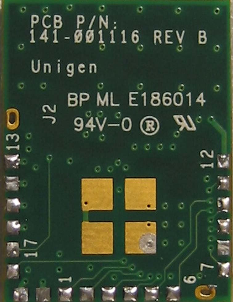
R8KUGWSX931
Nov 25, 2012900MHz Transceiver Module
Equipment Class
DTS - Digital Transmission System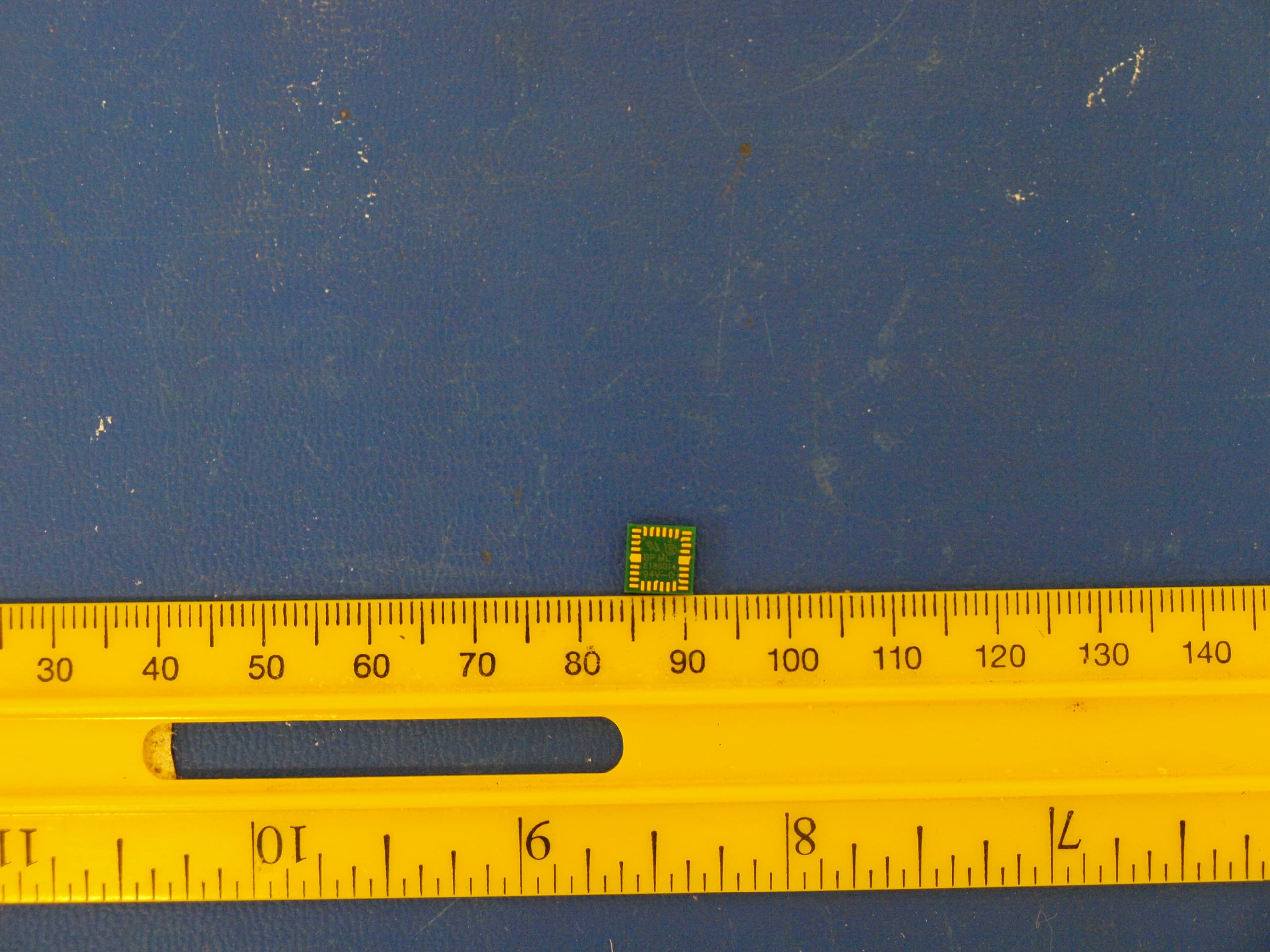
R8KUGWC821R
Jun 14, 2012NEMO BLUETOOTH RADIO MODULE
Equipment Class
DSS - Part 15 Spread Spectrum Transmitter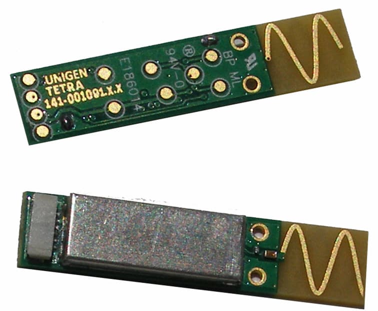
R8KUGWT1BL1
Jan 26, 2012TETRA Dual Mode Bluetooth Radio Module
Equipment Class
DSS - Part 15 Spread Spectrum Transmitter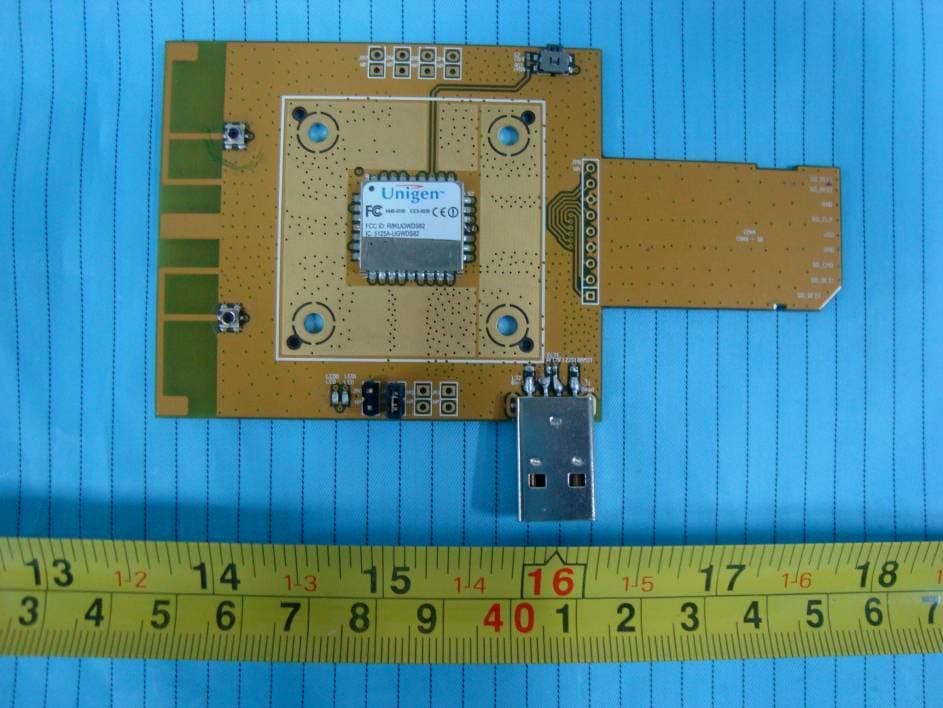
R8KUGWDS82
Jun 17, 2010802.11b/g/n WiFi Radio Module
Equipment Class
DTS - Digital Transmission System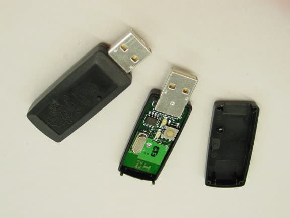
R8KUGQUBE1US
Dec 29, 2005USB Dongle
Equipment Class
DTS - Digital Transmission System