SQB-NIVISP9050103Amplified Radio Modem
HDJ WIRELESS ENTERPRISE, LLC d/b/a NIVIS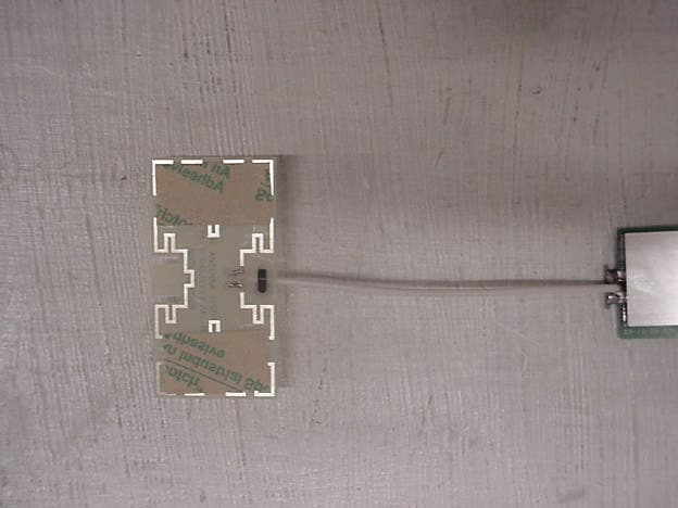
Click to zoom
Application Details
- Equipment Class
- DSS - Part 15 Spread Spectrum Transmitter
- Date of Grant
- Mar 22, 2005
- Application Purpose
- Original Equipment
- Date of Application
- Mar 22, 2005
- Equipment Note
- Amplified Radio Modem
- Frequency Range
- 910.50000000 - 927.49996200
- Country
- United States
Documents & Files
Document Text
Text extracted from the exhibit documents filed with the FCC. Open a document above to read the original.
Cover Letter(s)
March 10, 2005 Attention: Mr. William Graff ATCB Bill, Following is our response to your comments. RE: Nivis, LLC FCC ID: SQBNIVISP9050103 I have a few comments on this Application. Depending on your responses, kindly understand there may be additional comments. 1.) Please note the Confidentiality Request letter asks for the Manual to be held Confidential. This is not permitted under the FCC rules and interpretations, except in very specific circumstances. Kindly either remove the references to Manual from the Confidentiality Request letter or provide substantial justification for its inclusion. As in previous submittals, this product is a modular transmitter, and the manual is only intended for supply to the integrator. The end user will not receive these instructions. For that reason, the request to hold the manual in permanent confidentiality is made, to prevent users from accessing the commands provided exclusively for the integrator of the module. Nivis will supply a cover letter to the integrator instructing that all information contained in the integration manual is restricted from the end user, under FCC rules and interpretations. 2.) The photographs lump both Internal Photos and External Photos into one Exhibit. This is not permitted. The FCC database requires separated Internal and External photos without exception. FYI: May I suggest that all Module photos show all antennas and the device with RF shields intact as External photos, while all views with shields removed should be considered Internal Photos. This is generally the best practice. Photos have been changed and uploaded as you suggested. 3.) The Manual indicates the end user has access to RF channel selection, RF power control, modulation on/off, etc. This is a violation of 15.15(b) which reads in part: “Except as follows, an intentional or unintentional radiator must be constructed such that the adjustments of any control that is readily accessible by or intended to be accessible to the user will not cause operation of the device in violation of the regulations.” Since it appears that the end user can alter the characteristics of this device so that it will no longer operate as a spread spectrum frequency hopping transmitter, I do not see how this meets the requirements. See the definition of a Frequency Hopper as defined under 2.1(c) and review the Manual carefully. As stated in item 1, this manual is intended for the integrator only. These commands are for testing and design specifications while incorporating the module into the end product. The final version will operate as tested. 4.) I do not understand the method expressed in section 2.11 of the Test Report. Is the manufacturer dictating the measurement bandwidths (RBW and VBW) to be used during this measurement? The statement was a misprint. The RBW was set to 1% of the operating bandwidth. This has been corrected in the report. 5.) I am not convinced the 8dB duty cycle correction specified in your Test Report is valid. Consider the fact that a 1MHz RBW is specified for measurement above 1GHz. If I analyze the hop sequence provided, there are many instances when the carrier hop does not exceed 1MHz. Therefore I cannot be sure that the carrier will not add extra energy to average measurements at, say, the third, fourth or fifth harmonic. This difference may be critical for compliance with the provisions of 15.205. Your comments would be appreciated. My response is taken from FCC publication Number 575077. “If the dwell time (transmit time) of the Equipment Under Test (EUT) on a single channel, under normal operating conditions, is less than 100 ms, then an additional duty cycle correction may be mathematically applied to the measured average value. This correction is calculated from 20 log (dwell time/100ms). If the dwell time of the EUT on a single channel exceeds 100 (corrected from 199) ms, then this duty cycle correction is not applicable. The number of channels to which the EUT hops has no bearing on this calculation.” It is my understanding that this method is acceptable for all FHSS transmitters, regardless of number of channels, based upon time of occupancy of each channel, and we have followed that method in this instance. 6.) The hop sequence is not truly “pseudorandom”. Hops appear in groups of three which sequentially increment 910, 911, 912...927 MHz. Please review with your client. If this creates a significant design problem with your client, I will be happy to consult with the Commission for a “second opinion”. The client has responded to this by stating that they provided a pseudo-random hop table by mistake. Please disregard this list from the review. If you review the frequency to channel list, you will see that the frequency assignments per channel are assigned using a pseudo-random order. The client has chosen to assign the frequencies in a random order, then sequentially transmit each channel in order (0-49), thereby creating a pseudo random hop sequence of the frequencies, in this manner. 7.) FYI: Please remember that, by definition, the receiver must hop in synchronization with the transmitter. This is true with all frequency hopping spread spectrum devices. Thank you. 8.) The Theory of Operation in section 5.1.1 indicates this device operates outside of the 902- 928MHz band allowed for Unlicensed spread spectrum operations. Moreover, this device appears to operate outside of the requested frequency range requested on Form 731. Please address. The Theory of Operation has been corrected and uploaded to reflect 902-928 MHz. Please contact me with any further comments, Sincerely, Louis A. Feudi Operations Manager
Cover Letter(s)
CONFIDENTIALITY REQUEST Federal Communications Commission Date: January 27, 2005 Equipment Authorization Branch 7435 Oakland Mills Road Columbia, MD 21046 Gentlemen: Nivis, LLC respectfully requests confidentiality of certain materials provided with the submission of the RF –P9-05-01-03 Amplified radio Modem under FCC ID: SQB-NIVISP9050103 in accordance with FCC Regulations 0.459. The confidentiality request applies to the following: Parts List, Operational Descriptions, Schematics Block Diagrams, User’s Manual and Tune Up Procedures These items are considered as Trade Secrets and therefore public access to the proprietary material could possible result in duplication of equipment that could severely damage the company's business advantage. I appreciate your assistance in this matter. Sincerely, Name: Louis A. Feudi Signature: Title: Operations Manager Date: January 27, 2005
Cover Letter(s)
Date: January 31, 2005 AmericanTCB Gentlemen: Nivis, LLC is submitting their Amplified Radio Modem under FCC ID: SQB-NIVISP9050103 application to American TCB. Uploaded are 22 files for your review. While evaluating this application, please keep in mind that the modem has 2 antennas, a fractal and dual band pcs. In order to meet the requirements of FCC part 15C, the power level for each antenna will be unique. For the fractal antenna, the maximum conducted output power will be 21.11 dBm. For the dual band antenna, the maximum conducted output power will be 21.02 dBm. These settings will be preset at the factory, and will not be adjustable by the integrator above the maximum preset. Since the fractal antenna is soldered onto the board, and the dual band pcs antenna has a unique antenna connector, there will be no interchange of the antennas between units. Please contact me with any questions you may have regarding this application. I appreciate your assistance in this matter. Sincerely, Name: Louis A. Feudi Signature: Title: Operations Manager Date: January 31, 2005
Cover Letter(s)
American Telecommunications Certification Body Inc. 6731 Whittier Ave, McLean, VA 22101 March 4, 2005 RE: Nivis, LLC FCC ID: SQBNIVISP9050103 I have a few comments on this Application. Depending on your responses, kindly understand there may be additional comments. 1.) Please note the Confidentiality Request letter asks for the Manual to be held Confidential. This is not permitted under the FCC rules and interpretations, except in very specific circumstances. Kindly either remove the references to Manual from the Confidentiality Request letter or provide substantial justification for its inclusion. 2.) The photographs lump both Internal Photos and External Photos into one Exhibit. This is not permitted. The FCC database requires separated Internal and External photos without exception. FYI: May I suggest that all Module photos show all antennas and the device with RF shields intact as External photos, while all views with shields removed should be considered Internal Photos. This is generally the best practice. 3.) The Manual indicates the end user has access to RF channel selection, RF power control, modulation on/off, etc. This is a violation of 15.15(b) which reads in part: “Except as follows, an intentional or unintentional radiator must be constructed such that the adjustments of any control that is readily accessible by or intended to be accessible to the user will not cause operation of the device in violation of the regulations.” Since it appears that the end user can alter the characteristics of this device so that it will no longer operate as a spread spectrum frequency hopping transmitter, I do not see how this meets the requirements. See the definition of a Frequency Hopper as defined under 2.1(c) and review the Manual carefully. 4.) I do not understand the method expressed in section 2.11 of the Test Report. Is the manufacturer dictating the measurement bandwidths (RBW and VBW) to be used during this measurement? 5.) I am not convinced the 8dB duty cycle correction specified in your Test Report is valid. Consider the fact that a 1MHz RBW is specified for measurement above 1GHz. If I analyze the hop sequence provided, there are many instances when the carrier hop does not exceed 1MHz. Therefore I cannot be sure that the carrier will not add extra energy to average measurements at, say, the third, fourth or fifth harmonic. This difference may be critical for compliance with the provisions of 15.205. Your comments would be appreciated. 6.) The hop sequence is not truly “pseudorandom”. Hops appear in groups of three which sequentially increment 910, 911, 912...927 MHz. Please review with your client. If this creates a significant design problem with your client, I will be happy to consult with the Commission for a “second opinion”. 7.) FYI: Please remember that, by definition, the receiver must hop in synchronization with the transmitter. This is true with all frequency hopping spread spectrum devices. 8.) The Theory of Operation in section 5.1.1 indicates this device operates outside of the 902-928MHz band allowed for Unlicensed spread spectrum operations. Moreover, this device appears to operate outside of the requested frequency range requested on Form 731. Please address. William H. Graff President and Director of Engineering mailto: [email protected] The items indicated above must be submitted before processing can continue on the above referenced application. Failure to provide the requested information may result in application termination. z Page 2 March 4, 2005 Correspondence should be considered part of the permanent submission and may be viewed from the Internet after a Grant of Equipment Authorization is issued. Please do not respond to this correspondence using the email reply button. In order for your response to be processed expeditiously, you must submit your documents through the AmericanTCB.com website. Also, please note that partial responses increase processing time and should not be submitted. Any questions about the content of this correspondence should be directed to the sender.
External Photos
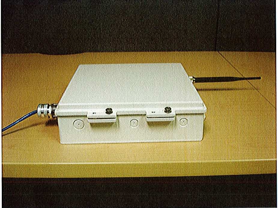
Photo 1.Top View of EUT With Shield in Place Photo 4.Dual Band Antenna Photo 5.Fractal Antenna
ID Label/Location Info
FCC LABEL 3 FCC LABEL A 1 1 12/07/2004 Title Size Document Number Rev Date: Sheet of NIVIS LLC 1.00 0.75 2.00 1.50
Internal Photos
Photo 2.Top View of EUT With Shield Removed Photo 3.Bottom View of EUT
Parts List/Tune Up Info
Nivis Radio Modem Calibration Procedure Version 1.0 Modified: December 3, 2004 Nivis Modem Tune-up Procedure Proprietary & Confidential Version 1.0 Revision History DateRevisionDescriptionAuthor 12/3/20041.0Calibration ProcedureRobert Assimiti Nivis Modem Tune-up Procedure Proprietary & Confidential Version 1.0 Table of Contents 1.Scope....................................................................................................................................1 2.Calibration Equipment......................................................................................................1 2.1.NivisLink Software (Calibration GUI).........................................................................1 2.2.Calibration and Test Equipment.................................................................................1 3.Automatic Frequency Control Calibration..................................................................4 3.1.Setup Diagram..............................................................................................................4 4. Assignment of ID and Temperature Compensation.....................................................6 4.1 Assignment of ID................................................................................................................6 4.2 Temperature Compensation............................................................................................6 Nivis Modem Tune-up Procedure Proprietary & Confidential Page 1 version 1.8.2 1. Scope The scope of this document is to describe the tune-up procedure undergone by each Nivis Radio Modem 2. Calibration Equipment 2.1. NivisLink Software (Calibration GUI) The NivisLink software is a LabView application that permits automatization of calibration and testing procedure of the Nivis radio modem. 2.1.1. Serial Port Setup • Initialize the NivisLink application • Select the “Serial” tab • Ensure that the settings in the “Port Configuration” section are as follows Com Port: correct COM port Baud Rate: 9600 Data bits: 8 Buffer size: 0 Stop bits: 1 bit Parity: no parity A screenshot of the “Serial” tab is presented in Figure 1. 2.2. Calibration and Test Equipment The following test equipment is necessary to support calibration procedures of the Nivis Radio Modem. Configuration details for each test are described under individual test headings. • Computer o NivisLink Calibration software o GPIB card • Frequency Counter (1GHz) • Serial Cable • GPIB Cable Nivis Modem Tune-up Procedure Proprietary & Confidential Page 2 version 1.8.2 • Power Supply/Battery Nivis Modem Tune-up Procedure Proprietary & Confidential Page 3 version 1.8.2 Nivis Modem Tune-up Procedure Proprietary & Confidential Page 4 version 1.8.2 Figure 1: Screenshot of Serial Tab of the NivisLink Application 3. Automatic Frequency Control Calibration After the manufacturing process the frequency of the RF transceiver must be correlated to an accurate reference frequency. This was traditionally accomplished manually with a trimmer capacitor. The NivisLink application permits automatic frequency control calibration excluding the necessity of a costly manual operation. 3.1. Setup Diagram Nivis Modem Tune-up Procedure Proprietary & Confidential Page 5 version 1.8.2 Computer Frequency Counter 5386A Frequency Counter GPIB Unit Under Test Serial Cable RF Cable 3.1.1. Connect the computer’s serial port to the Radio modem development board serial port through a serial cable. 3.1.2. Attach the RF output to the frequency counter input. 3.1.3. Make sure the appropriate channel is being used on the counter. The channel should work up to 1 GHz. Also ensure that the input to the frequency counter is protected to its maximum input power. 3.1.4. Power up the mother board/modem. 3.2. Procedure Connect to the radio modem through the serial port by pressing the “CONNECT (0xFFFFFFFF) button located in the “String to Send” section of the “SERIAL” tab page (NivisLink GUI). Once the “CONNECTED” button is highlighted, switch over to the tab entitled “Temperature Calibration”. The “Temperature Calibration” tab is depicted in Figure 2. Press the “Frequency Offset” button. This will set the radio modem in transmission at a low output power at a frequency of 915 MHz. The counter will display the frequency of the signal and than send the value to the NivisLink application via the GPIB. The frequency received will be displayed in the “UnComp CalFreq”. The offset between the frequency received and 915 Mhz will be displayed in the “UnComp Freq Error” tab and will be sent to the modem. The modem will adjust it’s transmit frequency according to the offset received and will re-transmit. This string of events is re-iterated until the frequency is within ± 500 Hz of 915 Mhz. Once a final frequency offset value is reached, the value is written in the modem’s calibration EEPROM. Nivis Modem Tune-up Procedure Proprietary & Confidential Page 6 version 1.8.2 Figure 2: Screenshot of Temperature Calibraion Tab of the NivisLink Application 4. Assignment of ID and Temperature Compensation 4.1 Assignment of ID Enter the desired serial number in the tab labeled “Write SN” and than press the “Write SN & DNA (0xF1)” button. The serial number will be stored in the calibration EEPROM of the modem, and will become the permanent ID of the modem. 4.2 Temperature Compensation Nivis Modem Tune-up Procedure Proprietary & Confidential Page 7 version 1.8.2 Using an accurate temperature sensor measure the ambient temperature of the modem. Enter the temperature value in the tab labeled “Ambient Temperature” and than use the “Send Temperature” button. The modem processor will write the value in the calibration EEPROM. This will serve as a temperature reference for the processor’s internal temperature sensor.
RF Exposure Info
RF EXPOSURE INFORMATION 5.1 RF Safety Requirements to 2.1091 for Mobile Transmitters The unit under evaluation has two external antennas. Nivis LLC calculated the MPE emission values for the EUT with each of the antennas. The maximum power density occurs when using the 1.73 dBi Fractal antenna. They used the formula shown in OET Bulletin 65 and calculated the minimum distance between antenna and unsuspecting user as 20 cm. Nivis LLC will sell the RF-P9-05-01-03 with one of the following antennas. MANUFACTURER TYPE OF ANTENNA MODELGAIN dB TYPE OR CONNECTOR Mobile Antennas NivisFractalNivis-Falcon1.73 dBSoldered to Antenna pad J3 ComtelcoDual Band PCS A113182BUnityReverse SMA Fractal Antenna Power Output The EUT’s maximum expected output power as shown in Section 2.6 was Frequency of Fundamental (MHz) Measurement (dBm)* Measurement (mW)* FCC Limit (Watt) 910.44720.86121.901.0 918.93721.11129.121.0 927.44020.88122.461.0 * Measurement includes 0.1 dB for cable loss The maximum EIRP expected for mobile installations is with the +1.73 dBi gain Fractal antenna. This would yield a maximum EIRP of 20.86 dBm + 1.73 dBi = +22.59 dBm. (The Comtelco Dual Band PCS antenna has a unity gain, therefore maximum EIRP is 21.02, as detailed in Table 3a.) 5.1 RF Safety Requirements to 2.1091 for Mobile Transmitters – Cont. The maximum EIRP for mobile installations may be expected to be Antilog (22.59 dBm/10) = 181.6 mW MPE Calculations The limits for this unit (uncontrolled exposure) are 1.0 mW/cm 2 . Taking the RF Denisty Field Equation: Mobile Installations S = 181.6/4*π* 20 2 S = 181.6/5026.55 S = .036 mW / cm 2 This is well below the maximum level of 1.0 mW / cm 2 All manual instructions will specify 20 cm for mobile installations
Test Report
Nivis, LLC FCC Part 15, Certification Application Amplified Radio Modem RF-P9-05-01-03 UST Project: 04-0282 Issue Date: January 21, 2005 I certify that I am authorized to sign for the manufacturer and that all of the statements in this report and in the Exhibits attached hereto are true and correct to the best of my knowledge and belief: UNITED STATES TECHNOLOGIES, INC. (AGENT RESPONSIBLE FOR TEST): By: Name: Louis A. Feudi __________ Title: Operations Manager Date: January 21, 2005 _ Nivis. LLC 900 Circle 75 Parkway, Suite 1700 Atlanta, GA 30339 By: Name: Title: Date: This report shall not be reproduced except in full. This report may be copied in part only with the prior written approval of U.S. Technologies. The results contained in this report are subject to the adequacy and representative character of the sample provided. FCC ID: SQB-NIVISP9050103 U.S. Technologies, Inc.FCC Part 15, Class B Certification Report Number:04-0282Issue Date: January 21, 2005 Customer: Nivis, LLC Model: Amplified Radio Modem RF-P9-05-01-03 Page 1 MEASUREMENT/TECHNICAL REPORT This report concerns (check one): Original grant X Class II change_____ Equipment type: Spread-Spectrum Frequency Hopping RF modem that operates in the 902-928 MHz ISM band Deferred grant requested per 47 CFR 0.457(d)(1)(ii)? yes_____ No X If yes, defer until:_________________ date N.A. agrees to notify the Commission by N.A. date of the intended date of announcement of the product so that the grant can be issued on that date. Report prepared by: United States Technologies, Inc. 3505 Francis Circle Alpharetta, GA 30004 Phone Number: (770) 740-0717 Fax Number: (770) 740-1508 FCC ID: SQB-NIVISP9050103 U.S. Technologies, Inc.FCC Part 15, Class B Certification Report Number:04-0282Issue Date: January 21, 2005 Customer: Nivis, LLC Model: Amplified Radio Modem RF-P9-05-01-03 Page 2 TABLE OF CONTENTS AGENCY AGREEMENT LETTER OF CONFIDENTIALITY SECTION 1 GENERAL INFORMATION 1.1Product Description 1.2Related Submittal(s) SECTION 2 TESTS AND MEASUREMENTS 2.1Configuration of Tested EUT 2.2Test Facility 2.3Test Equipment 2.4Modifications 2.5Test Procedure and Results 2.6Antenna Description 2.7Peak Power (Bandedge Antenna Conducted at Antenna Terminal) 2.8Antenna Conducted Spurious Emissions 2.9 Peak Radiated Spurious Emissions 2.10 Average Radiated Spurious Emissions 2.11 Minimum 20 dB Bandwidth 2.12 Number of Hopping Channels 2.13 Average Time of Occupancy per Channel 2.14 Power Line Conducted Emissions for Transmitter 2.15 Radiated Emissions for Digital Device & Receiver (47 CFR 15.109a) 2.16 Power Line Conducted Emissions for Digital Device and Receiver FCC Section 15.107 2.17 Channel Separation FCC ID: SQB-NIVISP9050103 U.S. Technologies, Inc.FCC Part 15, Class B Certification Report Number:04-0282Issue Date: January 21, 2005 Customer: Nivis, LLC Model: Amplified Radio Modem RF-P9-05-01-03 Page 3 LIST OF FIGURES AND TABLES FIGURES 1)Test Configuration 2) Photograph(s) for Spurious and Conducted Emissions 3) Peak Output Power 4) Conducted Spurious Emissions 5) Peak Radiated Spurious Emissions 6) 20 dB Bandwidth 7) Number of Hopping Channels TABLES 1)EUT and Peripherals 2) Test Instruments 3) Peak Power Output 4) Peak Radiated Spurious Emissions 5) Average Radiated Spurious Emissions 6) 20 dB Bandwidth 7) Number of Hopping Channels 8) Conducted Emissions 9) Radiated Emissions for Digital Device and Receiver FCC ID: SQB-NIVISP9050103 U.S. Technologies, Inc.FCC Part 15, Class B Certification Report Number:04-0282Issue Date: January 21, 2005 Customer: Nivis, LLC Model: Amplified Radio Modem RF-P9-05-01-03 Page 4 SECTION 1 GENERAL INFORMATION FCC ID: SQB-NIVISP9050103 U.S. Technologies, Inc.FCC Part 15, Class B Certification Report Number:04-0282Issue Date: January 21, 2005 Customer: Nivis, LLC Model: Amplified Radio Modem RF-P9-05-01-03 Page 5 GENERAL INFORMATION 1.1Product Description The Equipment Under Test (EUT) is the Nivis Amplified Radio Modem RF-P9-05-01-03. The EUT is a Spread- Spectrum Frequency Hopping RF Modem operating in the 902-928 MHz ISM band. The radio modem is designed for remote data acquisition systems. The RF-P9-05-01-03 radio modem exhibits the following features: • Low power consumption achievable by employing the ultra-low power MSP430F149 microprocessor which powers the RF section down through a digital output pin of the processor. Power-down current draw as low as 5 μA is achievable. • RF output of 23 dB achievable by employing the MAX2235 power amplifier • Exceptional -117 dB sensitivity achieved with an external LNA used in conjunction with Chipcon’s CC1020 RF transceiver • No additional processing entities are required for data acquisition since the modem can read digital and analog data from the surrounding world through 8 digital I/O lines and 2 analog lines • Communication with external processing entities is achieved serially either through a dedicated selectable baud-rate hardware UART at CMOS level or through a bit-banged I2C bus • Operates over the extended temperature range of -40º to +85º and 80% non-condensing humidity • Built in software protocol for error control and re-transmissions • Frequency hopping algorithm which employs 50 frequency channels equally distributed over the 902-928 MHz band • Compact size of 2” x 1.5” x 0.3” and weight of 0.8 oz (23 grams). • Over-the-air re-programming of the firmware possible since an on-board 64 kByte EEPROM provides enough storage capability for code hot-swapping • Integrated AFC (Automatic Frequency Correction) hardware and accompanying software algorithm excludes the need for a precise crystal operating over the extended temperature range • Connectivity is provided through two 12-pin .100 singe row headers • Two shields (one over the digital section and one over the RF section) greatly reduce radiated RF interfering emissions and improve RF immunity 1.2Related Submittal(s)/Grant(s) The EUT will be used to send/receive data. The transceiver presented in this report …
Text truncated - open the document above for the full version.
Test Report
FCC ID: SQB-NIVISP9050103 U.S. Technologies, Inc.FCC Part 15, Class B Certification Report Number:04-0282Issue Date: January 21, 2005 Customer: Nivis, LLC Model: Amplified Radio Modem RF-P9-05-01-03 Page 1 2.9Peak Radiated Spurious Emission in the Frequency Range 30 -25000 MHz (FCC Section 15.247(c)) The EUT was hop-stopped and when possible, placed into a continuous transmit mode of operation. A preliminary scan was performed on the EUT to determine frequencies that were caused by the transmitter portion of the product. Significant emissions that fell within restricted bands were then measured on an OAT’s site. Radiated measurements below 1 GHz were tested with a RBW = 120 kHz. Radiated measurements above 1 GHz were measured using a RBW = VBW = 1 MHz. The results of peak radiated spurious emissions falling within restricted bands are given in Table 4a –4g and Figure 5a – Figure 5ai. FCC ID: SQB-NIVISP9050103 U.S. Technologies, Inc. FCC Part 15, Class B Certification Report Number:04-0282Issue Date: January 21, 2005 Customer: Nivis, LLC Model: Amplified Radio Modem RF-P9-05-01-03 Page 2 Table 4a. PEAK RADIATED SPURIOUS EMISSIONS Low Channel Dual Band Antenna` Freq. (MHz) Test Data (dBm) @ 3m AF + CA - AMP (dB) Results (uV/m) 3m FCC Limits (uV/m) MARGIN BELOW FCC Limits (dB) 910.52-16.430.7 1156832.6-- 1821.06-22.6-6.9 7527.5 115683.323.7 2731.51-52.2-2.4 415.15000.021.6 3641.93-49.91.0 807.65000.015.8 4552.58-56.04.8 615.35000.018.2 5463.01-44.7**6.8 2853.8115683.332.2 6373.48-61.0**8.1 506.2115683.347.2 7283.96-57.7**9.9 914.85000.014.8 Data corrected by 1 dB for loss of high pass filter except for fundamental frequency ** Data conversion from 1 meter to 3 meters = -9.54 SAMPLE CALCULATION: RESULTS (uV/m @ 3m) = Antilog ((-22.6 + -6.9 + 107)/20) = 7527.5`` CONVERSION FROM dBm TO dBuV = 107 dB Tester Signature: Name: David Blethen FCC ID: SQB-NIVISP9050103 U.S. Technologies, Inc. FCC Part 15, Class B Certification Report Number:04-0282Issue Date: January 21, 2005 Customer: Nivis, LLC Model: Amplified Radio Modem RF-P9-05-01-03 Page 3 Figure 5a-1 Peak Radiated Spurious Emission 15.247(c) Low – Dual Band Fundamental FCC ID: SQB-NIVISP9050103 U.S. Technologies, Inc. FCC Part 15, Class B Certification Report Number:04-0282Issue Date: January 21, 2005 Customer: Nivis, LLC Model: Amplified Radio Modem RF-P9-05-01-03 Page 4 Figure 5a-2 Peak Radiated Spurious Emission 15.247(c) Low – Dual Band 2 nd Harmonic FCC ID: SQB-NIVISP9050103 U.S. Technologies, Inc. FCC Part 15, Class B Certification Report Number:04-0282Issue Date: January 21, 2005 Customer: Nivis, LLC Model: Amplified Radio Modem RF-P9-05-01-03 Page 5 Figure 5a-3 Peak Radiated Spurious Emission 15.247(c) Low – Dual Band 3 rd Harmonic FCC ID: SQB-NIVISP9050103 U.S. Technologies, Inc. FCC Part 15, Class B Certification Report Number:04-0282Issue Date: January 21, 2005 Customer: Nivis, LLC Model: Amplified Radio Modem RF-P9-05-01-03 Page 6 Figure 5a-4 Peak Radiated Spurious Emission 15.247(c) Low – Dual Band 4 rh Harmonic FCC ID: SQB-NIVISP9050103 U.S. Technologies, Inc. FCC Part 15, Class B Certification Report Number:04-0282Issue Date: January 21, 2005 Customer: Nivis, LLC Model: Amplified Radio Modem RF-P9-05-01-03 Page 7 Figure 5a-5 Peak Radiated Spurious Emission 15.247(c) Low – Dual Band 5 rh Harmonic FCC ID: SQB-NIVISP9050103 U.S. Technologies, Inc. FCC Part 15, Class B Certification Report Number:04-0282Issue Date: January 21, 2005 Customer: Nivis, LLC Model: Amplified Radio Modem RF-P9-05-01-03 Page 8 Figure 5a-6 Peak Radiated Spurious Emission 15.247(c) Low – Dual Band 6 rh Harmonic FCC ID: SQB-NIVISP9050103 U.S. Technologies, Inc. FCC Part 15, Class B Certification Report Number:04-0282Issue Date: January 21, 2005 Customer: Nivis, LLC Model: Amplified Radio Modem RF-P9-05-01-03 Page 9 Figure 5a-7 Peak Radiated Spurious Emission 15.247(c) Low – Dual Band 7 rh Harmonic FCC ID: SQB-NIVISP9050103 U.S. Technologies, Inc. FCC Part 15, Class B Certification Report Number:04-0282Issue Date: January 21, 2005 Customer: Nivis, LLC Model: Amplified Radio Modem RF-P9-05-01-03 Page 10 Figure 5a-8 Peak Radiated Spurious Emission 15.247(c) Low – Dual Band 8 rh Harmonic FCC ID: SQB-NIVISP9050103 U.S. Technologies, Inc. FCC Part 15, Class B Certification Report Number:04-0282Issue Date: January 21, 2005 Customer: Nivis, LLC Model: Amplified Radio Modem RF-P9-05-01-03 Page 11 Table 4b. PEAK RADIATED SPURIOUS EMISSIONS Mid Channel Du…
Text truncated - open the document above for the full version.
Contact Information
Applicant
Doug Johns
Technical Contact
U.S. TechnologiesLouis A Feudi
[email protected]770 740 0717
3505 Francis Circle · Alpharetta, Georgia · United States
Test Firm
US TechSandy McEnery
Technical Specifications
| # | Rule Parts | Frequency Range | Power Output |
|---|---|---|---|
| 1 | 15C | 910.5 MHz - 927.499962 MHz | 130.00 mW |
Other Applications from HDJ WIRELESS ENTERPRISE, LLC d/b/a NIVIS
SQB-NIVISMOD0004
May 09, 2011VN210 RF Modem
Equipment Class
DTS - Digital Transmission System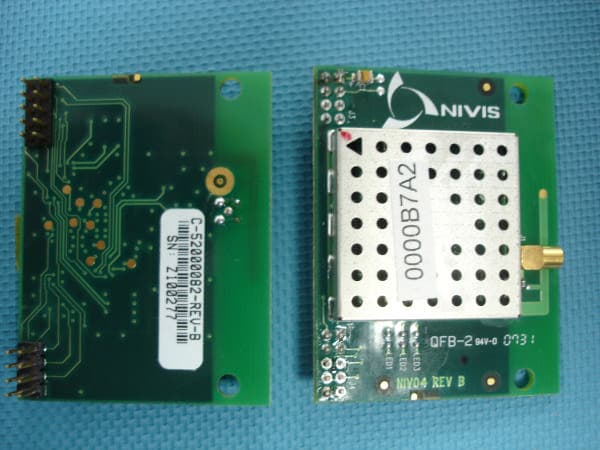
SQB-NIVISAN0010
Mar 27, 20082.4 GHz Ainode
Equipment Class
DTS - Digital Transmission System
SQB-NIVISNRD20101
Nov 06, 2006RF MODEM Module
Equipment Class
DSS - Part 15 Spread Spectrum Transmitter
SQB-NIVISRN0003
Sep 20, 2006Networking Device
Equipment Class
DSS - Part 15 Spread Spectrum Transmitter
SQB-NIVISSNF0002
May 23, 2006Networking Device
Equipment Class
DSS - Part 15 Spread Spectrum Transmitter