SQB-NIVISP9060101Transceiver Module
HDJ WIRELESS ENTERPRISE, LLC d/b/a NIVIS
Click to zoom
Application Details
- Equipment Class
- DSS - Part 15 Spread Spectrum Transmitter
- Date of Grant
- Jan 03, 2006
- Application Purpose
- Original Equipment
- Date of Application
- Jan 03, 2006
- Equipment Note
- Transceiver Module
- Frequency Range
- 910.50000000 - 927.50000000
- Country
- United States
Documents & Files
Document Text
Text extracted from the exhibit documents filed with the FCC. Open a document above to read the original.
Users Manual
RF Modem User’s Manual Version 1.1 Modified: January 4, 2006 User Manual Proprietary & Confidential Version 1.1 Revision History Date Revision Description Author 12.02.2005 1.0 Document Creation Szabi Zigovski 01.04.2006 1.1 Added section 6 “OEM Responsibility...” Szabi Zigovski User Manual Proprietary & Confidential Version 1.1 Table of Contents 1. Purpose and Scope of Document......................................................................... 1 2. Overview of the Radio Modem Hardware............................................................. 1 3. Operation of the Nivis Radio Modem ................................................................... 3 3.1. Getting started ...................................................................................................... 3 3.2 Read Calibration EEPROm ................................................................................... 4 3.3 Transmission ......................................................................................................... 5 3.4 Reception .............................................................................................................. 5 3.5 Modify Register Values .......................................................................................... 5 3.6 Additional Features................................................................................................ 5 4. RF Exposure Limit Warning ..................................................................................... 6 5. Compliance Statement (Part 15.19) ......................................................................... 6 6. OEM Responsibility to the FCC Rules and Regulations ........................................ 6 7. Warning (Part 15.21).................................................................................................. 7 User Manual Proprietary & Confidential Page 1 version 1.0 1. Purpose and Scope of Document This document was incepted in order to provide to the user clear guidelines regarding the usage of the Nivis RF-P9-06-01-01 modem. The scope of this document is limited to the first revision of the Nivis Amplified Radio Modem, part number RF-P9-06-01-01. 2. Overview of the Radio Modem Hardware The Nivis Radio modem RF-P9-06-01-01 is a frequency-hopping wireless module that allows wireless communication using a standard asynchronous serial data stream. The half-duplex transmission of the modem can sustain a continuous data stream at the specified data rate of 9600 bps. The pin-out of the Nivis radio modem is presented in the figure below. UTXD0 12 URXD0 11 GPIO1 10 GPIO2 9 TD I / TD O 8 TD I 7 TMS 6 TC K 5 RST/NMI 4 NC 3 GND 2 VCC 1 NC 14 INT1 15 INT2 16 SCL 17 SDA 18 ANALOG2 19 ANALOG1 20 NC 13 DIO4 21 DIO3 22 DIO2 23 DIO1 24 The radio modem consists of three functional entities: 1. Digital section – processor, EEPROMs, Power-on-reset circuitry 2. RF section – Chipcon RF transceiver and LNA 3. Power amplification section – MAX2235 power amplifier Power is supplied to the modem through pins 1 and 2. Pin 1 must be supplied with 3.6 Volts and powers the digital and RF functional entities of the modem. The modem has two internal 3.3 V LDOs which are powered through this pin. The LDOs require a dropout voltage of 200 mV. User Manual Proprietary & Confidential Page 2 version 1.0 All of the remaining pins of the modem are I/O lines of the processor. The voltage on any of the I/O lines should never exceed 3.3 V. Pins 11 and 12 are the TX and RX pins of UART 1. If connecting to the serial port of a PC, a level-shifting transceiver must be employed in order to provide the appropriate voltage levels on the RX and TX lines. A table of the radio modem pins is provided below, describing the purpose and functionality of the pins and the max voltage range on the pins. Pin number Pin name Function of pin Nominal voltage Max voltage 1 VCC Voltage supply 3.6 V 3.6 V 2 GND Ground pin SDA line of external I2C bus 3.3 V 3.6 V 3 NC N/A N/A N/A 4 RST/NMI Reset line of the processor 3.3 V 3.6 V 5 TCK JTAG line 3.3 V 3.6 V 6 TMS JTAG line 3.3 V 3.6 V 7 TDI JTAG line 3.3 V 3.6 V 8 TDI/TDO JTAG line 3.3 V 3.6 V 9 GPIO2 General purpose digital line of the processor 3.3 V 3.6 V 10 GPIO1 General purpose digital line of the processor 3.3 V 3.6 V 11 URXD0 RX line of UART 0 3.3 V 3.6 V 12 UTXD0 TX line of UART 0 3.3 V 3.6 V 13 NC N/A N/A N/A 14 NC N/A N/A N/A 15 INT1 Interrupt – digital line of processor 3.3 V 3.6 V 16 INT2 Interrupt – digital line of processor 3.3 V 3.6 V User Manual Proprietary & Confidential Page 3 version 1.0 17 SCL SCL line of external I2C bus – analog input to ADC 3.3 V 3.6 V 18 SDA SDA line of external I2C bus – analog input to ADC 3.3 V 3.6 V 19 AIN2 General purpose digital line of the processor – analog input to ADC 3.3 V 3.6 V 20 AIN1 General purpose digital line of the processor – analog input to ADC 3.3 V 3.6 V 21 DIO4 General purpose digital line of the processor – analog input to ADC 3.3 V 3.6 V 22 DIO3 General purpose digital line of the processor – analog input to ADC 3.3 V 3.6 V 23 DIO2 General purpose digital line of the processor – analog input to ADC 3.3 V 3.6 V 24 DIO1 General purpose digital line of the processor – analog input to ADC 3.3 V 3.6 V 3. Operation of the Nivis Radio Modem The NivisLink application was developed in order to exercise the features of the Nivis Radio modem. The NivisLink application is software application composed of a firmware hex file which is to be loaded onto the modem and a GUI that controls various features of the modem. 3.1. Getting started Install the NivisLink GUI on a PC and connect the serial port of the PC to the Nivis radio modem evaluation board RFB-01-01. Load the radio modem with the NivisLink hex file provided. User Manual Proprietary & Confidential Page 4 version 1.0 The figure below depicts the “Serial” tab of the NivisLink GUI. 3.2 Read Calibration EEPROm Note: The following procedure assumes that the modem used has already underg…
Text truncated - open the document above for the full version.
External Photos
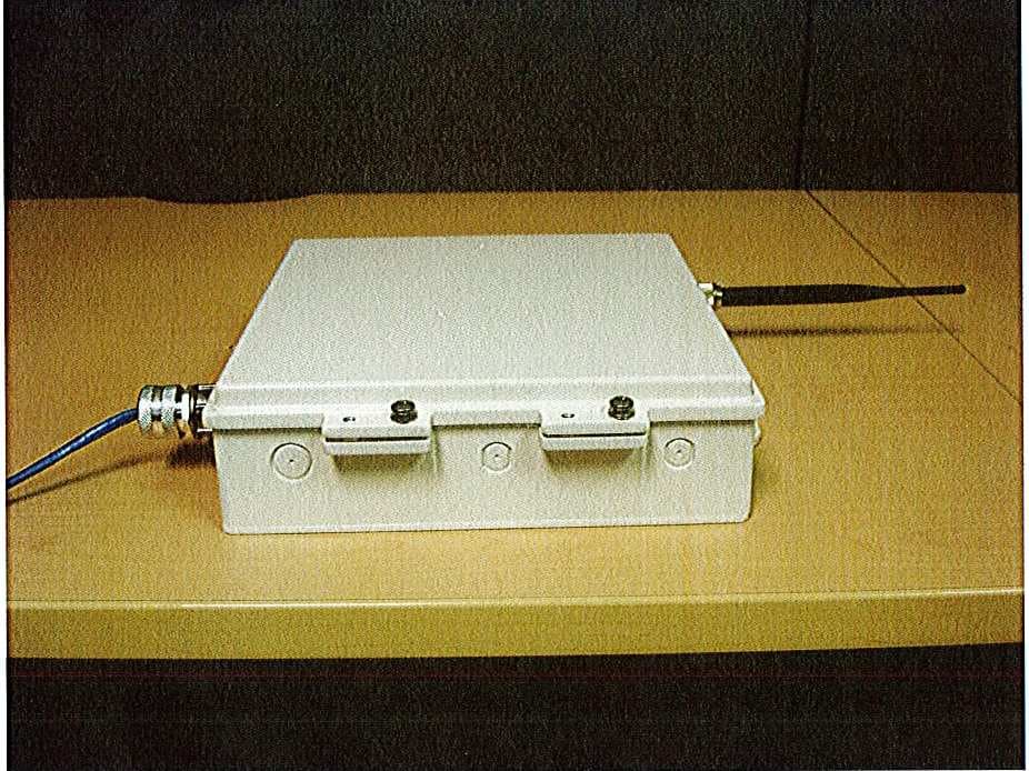
Nivis Focus RF Module FCC ID#: SQB-NIVISP9060101 SQB-NIVISP9060101 Photo One – External Front View of RF Module, with Antenna Flat Nivis Focus RF Module FCC ID#: SQB-NIVISP9060101 Photo Two – External RF Module with Antenna at Right Angle Nivis Focus RF Module FCC ID#: SQB-NIVISP9060101 Photo Three – External Close-up of Antenna Connection Nivis Focus RF Module FCC ID#: SQB-NIVISP9060101 Photo Four – External Close-up of FCC ID Label
ID Label/Location Info
REVISIONS REVSION DESCRIPTION DATE APPROVED 1 RELEASED FOR PROTOTYPE 11/29/05 1. MATERIAL: .002” THICK POLYESTER WITH 3M #400 OR #7921 ACRYLIC ADHESIVE a. BACKING: SILICONE RELEASE LINER b. FACE COLOR: WHITE WITH BLACK INK 2. ENVIRONMENTAL: a. TEMPERATURE RANGE: -40 º C TO +85 º C b. ADHESIVE, MATERIAL AND INK SHALL BE RESISTANCE TO UV DEGRADATION c. LIGHT AND HUMIDITY AS SPECIFIED IN UL 969 – OUTDOOR EXPOSURE TEST 3. FONT: ARIAL APPROXIMATELY AS SHOWN a. HEIGHT: .050” BOLD, .035 REGULAR 4. LABEL SIZE: 1.00” WIDE X .50” HIGH Machine readable Barcode Part 39 of the text above DRAWN BY: C.ENE DATE: 11/29/05 APPROVALS NIVIS LLC. ATLANTA , GEORGIA DOC CONTROL: DATE: TITLE: PURCH’G: DATE: DEV ENG: DATE: QUAL ASSR: DATE: LABEL, FCC NIVIS RADIO MFG ENG: DATE: SIZE A FCSM NO. DWG. NO. REV. 1 PRODUCT MGR: DATE: SCALE: NONE SHEET: 1 MODEL ID # : RF-P9-06-01-01 FCC ID: SQB-NIVISP9060101 XXXXXXXX SPECIFICATION CONTROL
ID Label/Location Info
REVISIONS REVSIONDESCRIPTIONDATEAPPROVED 1RELEASED FOR PROTOTYPE11/29/05 1. MATERIAL: .002” THICK POLYESTER WITH 3M #400 OR #7921 ACRYLIC ADHESIVE a.BACKING: SILICONE RELEASE LINER b.FACE COLOR: WHITE WITH BLACK INK 2. ENVIRONMENTAL: a.TEMPERATURE RANGE:-40 º C TO +85 º C b.ADHESIVE, MATERIAL AND INK SHALL BE RESISTANCE TO UV DEGRADATION c.LIGHT AND HUMIDITY AS SPECIFIED IN UL 969–OUTDOOR EXPOSURE TEST 3. FONT: ARIAL APPROXIMATELY AS SHOWN a. HEIGHT: .050” BOLD, .035 REGULAR 4. LABEL SIZE:1.50” WIDE X 1.10” HIGH DRAWN BY: C.ENEDATE: 11/29/05 APPROVALS NIVIS LLC. ATLANTA , GEORGIA DOC CONTROL:DATE: TITLE: PURCH’G:DATE: DEV ENG:DATE: QUAL ASSR:DATE: L ABEL, FCC NIVIS RADIO MFG ENG:DATE: SIZE A FCSM NO.DWG. NO.REV. 1 PRODUCT MGR:DATE:SCALE: NONESHEET: 1 SPECIFICATION CONTROL MODEL ID # : RF-P9-06-01-01 FCC ID:SQB-NIVISP9060101 THIS DEVICE COMPLIES WITH PART 15 OF THE FCC RULES. OPERATION IS SUBJECT TO THE FOLLOWING TWO CONDITIONS. (1) THIS DEVICE MAY NOT CAUSE HARMFUL INTERFERENCE, AND (2) THIS DEVICE MUST ACCEPT ANY INTERFERENCE RECEIVED, INCLUDING INTERFERENCE THAT MAY CAUSE UNDESIRED OPERATION.
Internal Photos
Nivis Focus RF Module FCC ID#: SQB-NIVISP9060101 Photo One – Internal Open for Inspection, with Shield Removed Nivis Focus RF Module FCC ID#: SQB-NIVISP9060101 Photo Two – Internal Close-Up/Shield Removed Nivis Focus RF Module FCC ID#: SQB-NIVISP9060101 Photo Three – Internal Close up of Antenna Connector Nivis Focus RF Module FCC ID#: SQB-NIVISP9060101 Photo Four – Internal RF Module PCB Board – Close-up/Flip Side
RF Exposure Info
Prediction of MPE limit at a given distance Equation from page 18 of OET Bulletin 65, Edition 97-01 where:S = power density P = power input to the antenna G = power gain of the antenna in the direction of interest relative to an isotropic radiator R = distance to the center of radiation of the antenna Maximum peak output power at antenna input terminal:27.00(dBm) Maximum peak output power at antenna input terminal:501.187(mW) Antenna gain(typical):2(dBi) Maximum antenna gain:1.585(numeric) Prediction distance:20(cm) Prediction frequency:915(MHz) MPE limit for uncontrolled exposure at prediction frequency:0.6(mW/cm^2) Power density at prediction frequency:0.158027(mW/cm^2) Maximum allowable antenna gain:7.8(dBi) 20cm =5.8dB Margin of Compliance at 2 4R PG S π =
Test Report
L.S. Compliance, Inc. W66 N220 Commerce Court Cedarburg, WI 53012 262-375-4400 Fax: 262-375-4248 COMPLIANCE TESTING OF : Focus RF Module Prepared For: Nivis, Incorporated Attention: Mr. Trae Harrison 900 Circle 75 Parkway, Suite 1700 Atlanta, GA 30339 Test Report Number: 305170-Tx-v0 Test Dates: November 10 TH Through November 14 TH , 2005 All results of this report relate only to the items that were tested. This report is not to be reproduced, except in full, without written approval of L. S. Compliance, Inc. L.S. Compliance, Inc. Page 2 of 45 Test Report Number: 305170-Tx-v0 Prepared For: Nivis, Incorporated Table of Contents Section Description Page Index 2 1 L. S. Compliance in Review 3 2 A2LA Certificate of Accreditation 4 3 Validation Letter-U.S. Competent Body for EMC Directive 89/336/EEC 5 4 Signature Page 6 5 Product and General Information 7 6 Introduction 7 7 Product Description 8 8 Test Requirements 9 9 Summary of Test Report 9 10 Radiated Emissions Test 10-20 11 Band-Edge Measurements 21 12 Conducted RF Emissions onto AC Power Line 22-26 13 Occupied Bandwidth 27-28 14 Power Output 15.247(b) 29-30 15 Spurious RF Emissions 15.247(d) 31-32 16 Minimum Channel Separation 33-36 17 Channel Occupancy 37-38 18 Frequency and Power Stability requirements 39 19 Pseudorandom Hopping Pattern and Equal Channel Usage 40 20 Receiver Synchronization and Receiver Input Bandwidth 40 21 MPE Calculations 41 Appendix A Test Equipment List 42 B Antenna Specification 43 C Firmware and Setup Instructions 44-45 L.S. Compliance, Inc. Page 3 of 45 Test Report Number: 305170-Tx-v0 Prepared For: Nivis, Incorporated 1. L. S. Compliance In Review L.S. Compliance - Accreditations and Listing’s As an EMC Testing Laboratory, our Accreditation and Assessments are recognized through the following: A2LA – American Association for Laboratory Accreditation Accreditation based on ISO/IEC 17025 : 1999 with Electrical (EMC) Scope of Accreditation A2LA Certificate Number: 1255.01 Federal Communications Commission (FCC) – USA Listing of 3 Meter Semi-Anechoic Chamber based on Title 47 CFR – Part 2.948 FCC Registration Number: 90756 Industry Canada On file, 3 Meter Semi-Anechoic Chamber based on RSS-212 – Issue 1 File Number: IC 3088-A On file, 3 and 10 Meter OATS based on RSS-212 – Issue 1 File Number: IC 3088 U. S. Conformity Assessment Body (CAB) Validation Validated by the European Commission as a U. S. Competent Body operating under the U. S. /EU, Mutual Recognition Agreement (MRA) operating under the European Union Electromagnetic Compatibility –Council Directive 89/336/EEC, Article 10.2. Date of Validation: January 16, 2001 Validated by the European Commission as a U.S. Notified Body operating under the U.S./EU, Mutual Recognition Agreement (MRA) operating under the European Union Telecommunication Equipment – Council Directive 99/5/EC, Annex V. Date of Validation: November 20, 2002 Notified Body Identification Number: 1243 L.S. Compliance, Inc. Page 4 of 45 Test Report Number: 305170-Tx-v0 Prepared For: Nivis, Incorporated 2. A2LA Certificate of Accreditation L.S. Compliance, Inc. Page 5 of 45 Test Report Number: 305170-Tx-v0 Prepared For: Nivis, Incorporated 3. Validation Letter – U.S. Competent Body for EMC Directive 89/336/EEC L.S. Compliance, Inc. Page 6 of 45 Test Report Number: 305170-Tx-v0 Prepared For: Nivis, Incorporated 4. Signature Page Prepared By: December 2, 2005 Teresa A. White, Document Coordinator Date Tested By: December 2, 2005 Abtin Spantman, EMC Engineer Date Approved By: December 2, 2005 Brian E. Petted, VP of Engineering Date L.S. Compliance, Inc. Page 7 of 45 Test Report Number: 305170-Tx-v0 Prepared For: Nivis, Incorporated 5. Product and General Information Manufacturer: Nivis Incorporated Date(s) of Test: November 10 TH through November 14 TH , 2005 Test Engineer(s): Tom Smith √ Abtin Spantman Ken Boston Model #: Focus RF Module Board Serial #: 3AC5, 3A51 and 3AC9 Voltage: 3.6 VDC Operation Mode: Normal, continuous transmit, and ‘Hopping’ mode 6. Introduction Between November 10 TH and November 14 TH , 2005, a series of Conducted and Radiated RF Emission tests were performed on three samples of the Nivis RF modules, Model type “Focus RF Module”, Serial Numbers: 3AC5 (coded for test modes), 3AC9 and 3A51 (coded for frequency hopping communication), here forth collectively referred to as the “Equipment Under Test” or “EUT”. These tests were performed using the procedures outlined in ANSI C63.4-2003 for intentional radiators, and in accordance with the limits set forth in FCC Part 15.247 (Industry Canada RSS-210) for a low power transmitter. These tests were performed by Abtin Spantman, EMC Engineer of L.S. Compliance, Incorporated. All Radiated and Conducted RF Emission tests were performed upon the EUT to measure the emissions in the frequency bands described in FCC Title 47 CFR Part 15, including 15.35, 15.209, 15.247 and Industry Canada RSS-210 to determine whether these emissions are below the limits expressed within the standards. These tests were performed in accordance with the procedures described in the American National Standard for methods of measurement of Radio- Noise Emissions from Low-Voltage Electrical and Electronic Equipment in the Range of 9 kHz to 40 GHz (ANSI C63.4-2003). Another document used as a reference for the EMI Receiver specification was the Comite International Special Des Perturbations Radioelelectriques (CISPR) Number 16-1, 2003. All tests were performed at L.S. Compliance, Inc., in Cedarburg, Wisconsin, unless otherwise noted. L.S. Compliance, Inc. Page 8 of 45 Test Report Number: 305170-Tx-v0 Prepared For: Nivis, Incorporated 7. Product Description The Nivis “Focus Module” is a modular transceiver radio designed to operate as a Modem in electric meter applications. This module will use an external antenna to communicate with a network of electric meters and other Modem devices. The transceiver module is designed to operate as a frequency-hopper on 50 chan…
Text truncated - open the document above for the full version.
Test Setup Photos
Nivis SQB-NIVIS9060101 TEST SETUP PHOTOS View of the EUT setup in vertical orientation View of the EUT setup in Horizontal orientation View of the EUT setup in Side orientation View of the EUT setup in Vertical orientation on the test pedestal. View of the EUT setup during the Conducted Emissions Test
Contact Information
Applicant
Doug Johns
Test Firm
LS Research, LLCRyan Urness
Technical Specifications
| # | Rule Parts | Frequency Range | Power Output |
|---|---|---|---|
| 1 | 15C | 910.5 MHz - 927.5 MHz | 366.00 mW |
Other Applications from HDJ WIRELESS ENTERPRISE, LLC d/b/a NIVIS
SQB-NIVISMOD0004
May 09, 2011VN210 RF Modem
Equipment Class
DTS - Digital Transmission System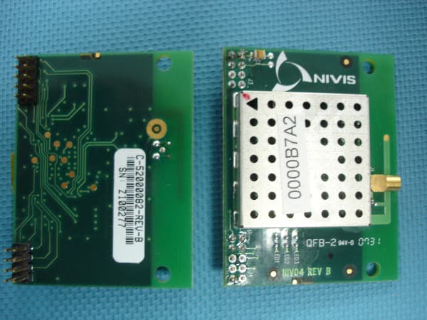
SQB-NIVISAN0010
Mar 27, 20082.4 GHz Ainode
Equipment Class
DTS - Digital Transmission System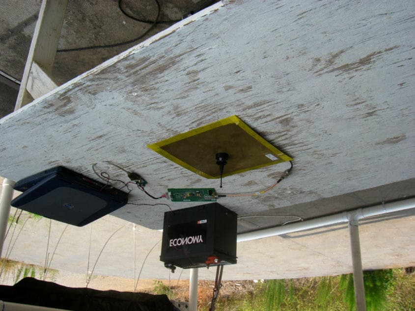
SQB-NIVISNRD20101
Nov 06, 2006RF MODEM Module
Equipment Class
DSS - Part 15 Spread Spectrum Transmitter
SQB-NIVISRN0003
Sep 20, 2006Networking Device
Equipment Class
DSS - Part 15 Spread Spectrum Transmitter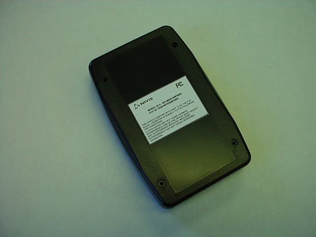
SQB-NIVISSNF0002
May 23, 2006Networking Device
Equipment Class
DSS - Part 15 Spread Spectrum Transmitter