T7V1740ABluetooth LE Module
Panasonic Industrial Devices Europe GmbH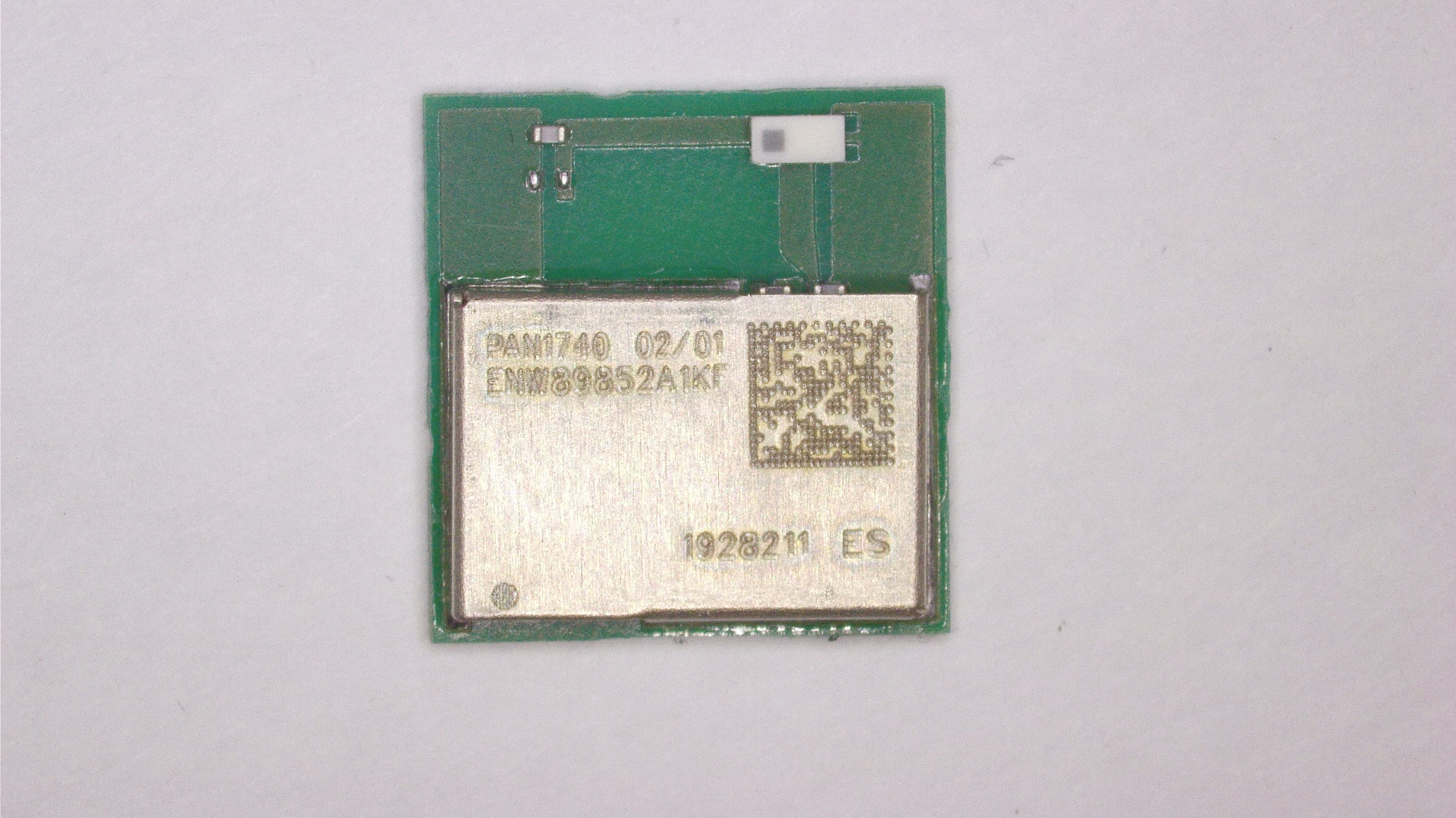
Click to zoom
Application Details
- Equipment Class
- DTS - Digital Transmission System
- Date of Grant
- May 13, 2020
- Application Purpose
- Original Equipment
- Date of Application
- May 13, 2020
- Equipment Note
- Bluetooth LE Module
- Frequency Range
- 2402.00000000 - 2480.00000000
- Country
- Germany
Documents & Files
Document Text
Text extracted from the exhibit documents filed with the FCC. Open a document above to read the original.
Users Manual
Wireless Connectivity PAN1740A Bluetooth ® Low Energy Module Module Integration Guide Rev. 1.1 PAN1740A Bluetooth Module 1 About This Document Module Integration Guide Rev. 1.1 Page 2 of 44 Overview The PAN1740A is an optimized version of the PAN1740, offering a reduced boot time and supporting up to eight connections. It has a fully integrated radio transceiver and baseband processor for Bluetooth ® 5 Low Energy (LE). It can be used as a stand-alone application processor or as a data pump in hosted systems. The device is optimized for remote control units (RCU) requiring support for voice commands and motion/gesture recognition. Its integrated Audio Unit (AU) offers easy interface for MEMS microphones over PDM, external codecs over PCM/I 2 S, and a Sample Rate Converter unit. The Bluetooth LE firmware includes the L2CAP service layer protocols, Security Manager (SM), Attribute Protocol (ATT), the Generic Attribute Profile (GATT), and the Generic Access Profile (GAP). All profiles published by the Bluetooth SIG as well as custom profiles are supported. The transceiver interfaces directly to the antenna and is fully compliant with the Bluetooth 5 standard. The PAN1740A has dedicated hardware for the Link Layer implementation of Bluetooth LE and interface controllers for enhanced connectivity capabilities. Features • Pre-programmed Bluetooth/MAC address • Includes 16 MHz and 32 768 kHz crystal calibrated up to 1 ppm • Single mode Bluetooth 5 System-on-Chip • Programmable ARM ® Cortex ® -M0 CPU • Autonomous Bluetooth LE stand-alone operation • Bluetooth 5 (LE) embedded GATT profile (LE single mode) • Dimensions: 9 mm x 9.5 mm x 1.8 mm (SMD package with antenna) • Less than a few μA in low power modes • Integrated shielding to resist EMI • No external components needed Characteristics • Peak power consumption: 4.9 mA (Rx and Tx) • Link budget: 93 dB (Rx sensitivity: -93 dBm, Tx sensitivity 0 dBm) • Operating temperature range -40 °C to 85 °C Block Diagram PAN1740A Bluetooth Module 1 About This Document Module Integration Guide Rev. 1.1 Page 3 of 44 By purchase of any of the products described in this document the customer accepts the document's validity and declares their agreement and understanding of its contents and recommendations. Panasonic Industrial Devices Europe GmbH (Panasonic) reserves the right to make changes as required at any time without notification. Please consult the most recently issued Module Integration Guide before initiating or completing a design. © Panasonic Industrial Devices Europe GmbH 2020. This specification sheet is copyrighted. Reproduction of this document is permissible only if reproduction is without alteration and is accompanied by all associated warranties, conditions, limitations, and notices. Do not disclose it to a third party. All rights reserved. This Module Integration Guide does not lodge the claim to be complete and free of mistakes. Engineering Samples (ES) If Engineering Samples are delivered to the customer, these samples have the status “Engineering Samples”. This means that the design of this product is not yet concluded. Engineering Samples may be partially or fully functional, and they may differ from the published Product Specification. Engineering Samples are not qualified and they are not to be used for reliability testing or series production. Disclaimer The customer acknowledges that samples may deviate from the Module Integration Guide and may bear defects due to their status of development and the lack of qualification mentioned above. Panasonic rejects any liability or product warranty for Engineering Samples. In particular, Panasonic disclaims liability for damages caused by: The use of the Engineering Sample other than for evaluation purposes, particularly the installation or integration in another product to be sold by the customer, Deviation or lapse in function of the Engineering Sample, Improper use of the Engineering Sample. Panasonic Industrial Devices Europe GmbH disclaims any liability for consequential and incidental damages. In case of any queries regarding the Engineering Samples, please contact your local sales partner or the related product manager. The information contained herein is presented only as guidance for Product use. No responsibility is assumed by Panasonic for any infringement of patents or any other intellectual property rights of third parties that may result from the use of Product. No license to any intellectual property right is granted by this document, whether express or implied, by estoppel or otherwise. Description of hardware, software, and other information in this document is only intended to illustrate the functionality of the referred Panasonic product. It should not be construed as guaranteeing specific functionality of the product as described or suitable for a particular application. Any provided (source) code shall not be used or incorporated into any products or systems whose manufacture, use or sale is prohibited under any applicable laws or regulations. Any outlined or referenced (source) code within this document is provided on an “as is” basis without any right to technical support or updates and without warranty of any kind on a free of charge basis according to § 516 German Civil Law (BGB) including without limitation, any warranties or conditions of title, non infringement, merchantability, or fitness for a particular purpose. Customer acknowledges that (source) code may bear defects and errors. PAN1740A Bluetooth Module 1 About This Document Module Integration Guide Rev. 1.1 Page 4 of 44 The third-party tools mentioned in this document are offered by independent third-party providers who are solely responsible for these products. Panasonic has no responsibility whatsoever for the performance, product descriptions, specifications, referenced content, or any and all claims or representations of these third-party providers. Panasonic makes no warranty whatsoever, neith…
Text truncated - open the document above for the full version.
Cover Letter(s)
CONFIDENTIALITY REQUEST for Certification Service in USA Federal Communication Commission Equipment Authorization Division, Application Processing Branch 7435 Oakland Mills Road Columbia, MD 21048 2020-05-06 TO WHOM IT MAY CONCERN Pursuant to Paragraphs §0.457 and 0.459 of the Commission’s Rules (47 C.F.R.) and Section §552(b)(4) of the Freedom of Information Act, we requests confidentiality for the following products: FCC ID Number Product Title/Model T7V1740A PAN1740A For the product stated above, we request permanent confidentiality for exhibits which contain Operational Description, Block Diagram, Schematics, Parts Lists or Tune Up Information. The above exhibits contain our trade secrets and proprietary information that could be of benefit to our competitors. If you have any questions, please feel free to contact me at the address shown below. Sincerely, (signed) Name: Olaf Knoth Company: Panasonic Industrial Devices Europe GmbH Address: Zeppelinstraße 19, 21337 Lüneburg Phone: +49 4131 899 257 Email: [email protected]
Cover Letter(s)
Federal Communication Commission Equipment Authorization Division, Application Processing Branch 7435 Oakland Mills Road Columbia, MD 21048 Certification and Engineering Bureau Industry Canada Spectrum Engineering Branch 3701 Carling Avenue, Building 94 Ottawa, Ontario K2H 8S2 Subject: FCC / ISED Modular Approval Statement FCC ID: Only applicable for ISED certification: IC Company Number: UPN: HVIN: (Hardware Version Identification Number) PMN: (Product Marketing Name) HMN: (Host Marketing Name) FVIN: (Firmware Version Identification Number) TO WHOM IT MAY CONCERN Pursuant to Paragraphs RSP-100 Issue 10 November 2014 Item 7.3 and CFR § 15.212, we herewith declare for our module. Modular approval requirement Yes No * (a) The radio elements must have the radio frequency circuitry be shielded. Physical/discrete and tuning capacitors may be located external to the shield, but must be on the module assembly. *Please provide a detailed explanation if the answer is “No.”: (b) The module shall have buffered modulation/data input(s) (if such inputs are provided) to ensure that the module will comply with the requirements set out in the applicable RSS standard under conditions of excessive data rates or over-modulation. *Please provide a detailed explanation if the answer is “No.”: (c) The module shall have its own power supply regulation on the module. This is to ensure that the module will comply with the requirements set out in the applicable standard regardless of the design of the power supplying circuitry in the host device which houses the module. *Please provide a detailed explanation if the answer is “No.”: (d) The module shall comply with the provisions for external power amplifiers and antennas detailed in this standard. The equipment certification submission shall contain a detailed description of the configuration of all antennas that will be used with the module. *Please provide a detailed explanation if the answer is “No.”: Yes No * (e) The module shall be tested for compliance with the applicable standard in a stand-alone configuration, i.e. the module must not be inside another device during testing. *Please provide a detailed explanation if the answer is “No.”: (f) The module shall comply with the Category I equipment labeling requirements and CFR § 15.212(a)(1)(vi). *Please provide a detailed explanation if the answer is “No.”: (g) The module shall comply with applicable RSS-102 exposure requirements and any applicable FCC RF exposure requirement which are based on the intended use/configurations. *Please provide a detailed explanation if the answer is “No.”: Only applicable for ISED certification: (h) Is the modular device for an Industry Canada licensed exempt service? (i) The modular transmitter complies with all applicable FCC rules. Instructions for maintaining compliance are given in the user instructions. If you have any questions, please feel free to contact us at the address shown below Be st Regards, Company Name: Ph one: Company Address: Fa x: Email: Contact Name: Signature: Si gnature Date: INF O for applicant: LMA may be granted when one or more of the requirements in the table above cannot be demonstrated. LMA will also be issued in those instances where applicants can demonstrate that they will retain control over the final installation of the device, such that compliance of the end product is assured. In such cases, an operating condition on the LMA for the module must state that the module is only approved for use when installed in devices produced by a specific manufacturer. When LMA is sought, the application for equipment certification must specifically state how control of the end product, into which the module will be installed, will be maintained, such that full compliance of the end product is always ensured. 2019-03-25
ID Label/Location Info
PAN1740A Bluetooth Module 3 Detailed Description Product Specification Rev. 1.0 Page 23 of 41 3.4 Case Marking Example: 1 2 3 4 5 6 7 8 9 Model name Hardware/software version Order number IC ID Lot code Engineering sample marking, if applicable FCC ID Marking for Pin 1 2D barcode, for internal usage only • Dimensions: 9 mm x 9.5 mm x 1.8 mm (SMD package with antenna)
RF Exposure Info
BNetzA - CAB - 02/21 - 102 D - P L - 1 2 0 7 6 - 0 1 - 0 3 SAR Test exclusion documentation according to FCC KDB 447498, RSS-102 Report identification number: 1-9205/19-01-09-A Exclusion (FCC_ISED) contains the module with the following certification numbers FCC ID T7V1740A ISED number 216Q-1740A HVIN (Hardware Version Identification Number) ENW89852A1KF PMN (Product Marketing Name) PAN1740A FVIN (Firmware Version Identification Number) ROM Dialog DA14585 HMN (Host Marketing Name) -/- This report is electronically signed and valid without handwriting signature. For verification of the electronic signatures, the public keys can be requested at the testing laboratory. Document authorised: p.o. Alexander Hnatovskiy Marco Scigliano Lab Manager Testing Manager Radio Communications & EMC Radio Communications & EMC Test report no.: 1-9205/19-01-09-A © CTC advanced GmbH Page 2 of 2 EUT technologies: Technologies: Max. rated power: (AVG) Max. gain: Min. pathloss: Bluetooth LE Declared: max 0 dBm -1.7 dBi 0 dB (if applicable) Note: Bluetooth LE test results see CTC advanced test report 1-9205/19-02-03 and for antenna gain the WM PAN1740_1740A Module Integration Guide_rev000.pdf document. SAR test exclusion according to KDB447498 (General RF Exposure Guidance v06) Equation from Chapter 4.3.1: Standalone SAR test exclusion considerations page 11 and ff. (1) Standalone SAR test exclusion for 100 MHz to 6 GHz at test separation distances ≤ 50mm ( Threshold 1-g;10-g ) × d seperation / f 0.5 where Threshold 1-g;10-g is 3 for 1-g; 7.5 for 10-g d seperation is the min. test separation distance; 5mm is used if the distance is less f is the RF channel transmit frequency The table below gives the calculated maximal power that could be used for source based time averaged conducted or radiated power, adjusted for tune up tolerance. If this is at or below the calculated value the DUT is exempted from SAR evaluation. frequency d separation Powerlimit [MHz] [mm] [mW] [dBm] [mW] 2450.00 5 3 9.58 0.00 1.00 yes Threshold 1-g Exclusion P max-declared SAR test exclusion according to RSS-102 Issue 5 Section 2.5.1/Table 1 The table below gives the calculated maximal power that could be used for source based time averaged conducted or radiated power, adjusted for tune up tolerance. If this is at or below the calculated value the DUT is exempted from SAR evaluation. frequencyd separation Powerlimit [MHz][mm][mW][dBm][mW] 2450.0051 g 4.002.001.58yes tissue volume P max-declared Exclusion The limits above are defined for body worn application and therefore cover all use cases.
Test Report
BNetzA - CAB - 02/21 - 102 TEST REPORT Test report no.: 1-9205/19-02-03 Testing laboratory Applicant CTC advanced GmbH Untertuerkheimer Strasse 6 – 10 66117 Saarbruecken / Germany Phone: + 49 681 5 98 - 0 Fax: + 49 681 5 98 - 9075 Internet: http://www.ctcadvanced.com e-mail: [email protected] Accredited Testing Laboratory: The testing laboratory (area of testing) is accredited according to DIN EN ISO/IEC 17025 (2005) by the Deutsche Akkreditierungsstelle GmbH (DAkkS) The accreditation is valid for the scope of testing procedures as stated in the accreditation certificate starting with the registration number: D-PL-12076-01. Panasonic Industrial Devices Europe GmbH Zeppelinstrasse 19 21337 Lüneburg / GERMANY Phone: +49-4131-899-0 Contact: Marcus Nottorf e-mail: [email protected] Phone: +49 41 31 89 94 35 Manufacturer Panasonic Industrial Devices Slovakia s.r.o Tovarenska 13 06401 Stara Lubovna / SLOVAK REPUBLIC Test standard/s FCC - Title 47 CFR Part 15 FCC - Title 47 of the Code of Federal Regulations; Chapter I; Part 15 - Radio frequency devices RSS - 247 Issue 2 Digital Transmission Systems (DTSs), Frequency Hopping Systems (FHSs) and Licence - Exempt Local Area Network (LE-LAN) Devices For further applied test standards please refer to section 3 of this test report. Test Item Kind of test item: Bluetooth Low Energy Module Model name: PAN1740A FCC ID: T7V1740A IC: 216Q-1740A Frequency: DTS band 2400 MHz to 2483.5 MHz Technology tested: Bluetooth ® LE Antenna: Internal ceramic antenna Power supply: 3.0 V DC by external power supply Temperature range: -40°C to +85°C This test report is electronically signed and valid without handwritten signature. For verification of the electronic signatures, the public keys can be requested at the testing laboratory. Test report authorized: Test performed: David Lang Mihail Dorongovskij Lab Manager Lab Manager Radio Communications Radio Communications Test report no.: 1-9205/19-02-03 © CTC advanced GmbH Page 2 of 50 1 Table of contents 1 Table of contents ............................................................................................................................................. 2 2 General information ......................................................................................................................................... 3 2.1 Notes and disclaimer ............................................................................................................................ 3 2.2 Application details ................................................................................................................................ 3 2.3 Test laboratories sub-contracted ......................................................................................................... 3 3 Test standard/s, references and accreditations .............................................................................................. 4 4 Test environment ............................................................................................................................................. 5 5 Test item .......................................................................................................................................................... 5 5.1 General description ............................................................................................................................... 5 5.2 Additional information .......................................................................................................................... 5 6 Sequence of testing ......................................................................................................................................... 6 6.1 Sequence of testing radiated spurious 9 kHz to 30 MHz ..................................................................... 6 6.2 Sequence of testing radiated spurious 30 MHz to 1 GHz .................................................................... 7 6.3 Sequence of testing radiated spurious 1 GHz to 18 GHz ..................................................................... 8 6.4 Sequence of testing radiated spurious above 18 GHz ......................................................................... 9 7 Description of the test setup.......................................................................................................................... 10 7.1 Shielded semi anechoic chamber ....................................................................................................... 11 7.2 Shielded fully anechoic chamber ........................................................................................................ 12 7.3 Radiated measurements > 18 GHz ...................................................................................................... 13 7.4 Conducted measurements Bluetooth system .................................................................................... 14 7.5 AC conducted ...................................................................................................................................... 15 8 Measurement uncertainty .............................................................................................................................. 16 9 Summary of measurement results ................................................................................................................ 17 10 Additional comments .............................................................................................................................. 18 11 Measurement results .............................................................................................................................. 19 11.1 System gain ..................................................................................................................................... 19 11.2 Power spectral density .....................................................................…
Text truncated - open the document above for the full version.
Test Report
Measurement Results 1-9205/19-02-03_log1_conducted Test logging This addendum is electronically signed and valid without handwritten signature. For verification of the electronic signatures, the public keys can be requested at the testing laboratory. Document authorized: Mihail Dorongovskij Lab Manager Radio Communications & EMC CTC advanced GmbHUntertuerkheimer Strasse 6-10 66117 Saarbruecken / Germany Phone: +49 681 5 98 - 0 Fax: +49 681 5 98 - 9075 web: ctcadvanced.com e-mail: [email protected] Table of Content IUT Summary3 1. Common2G4 Peak Output Power conducted 3MHz_3MHz ~ BT LE 1 Msps4 2. FCC Part 15.247 Maximum Peak Conducted Output Power DTS ~ BT LE 1 Msps8 3. FCC Part 15.247 Bandwidth 6dB DTS ~ BT LE 1 Msps15 4. FCC Part 15.247 Peak Power Spectral Density DTS ~ BT LE 1 Msps19 5. FCC Part 15.247 Bandwidth 99PCT-20dB ~ BT LE 1 Msps23 6. FCC Part 15.247 TX Spurious Conduced ~ BT LE 1 Msps30 7. FCC Part 15.247 Restricted Band Edge Conducted Peak DTS ~ BT LE 1 Msps34 Document No. 1-9205/19-02-03_log1_conducted2/36 IUT Summary IUT DEFINITION & Common settings Manufacturer Panasonic Industrial Devices Europe GmbH Type PAN1740A Serial No. | Setup No.NI | 1.0 SW Version | HW Version 01 | 02 Comment 1 | 2 | Tlow | Tmid | Thigh [°C] -40 | 20 | 85 Vlow | Vmid | Vhigh [V] @Imax [A] 5.0 | 5.0 | 5.0 @1 Auto Control enabled Power Supply | Climatic BoxNo | No Antenna Gain [dBi]0 Additional Path Loss [dB]1.2 IUT Common Settings BT Low Energy Intermodulation Value N3 Image Freq. Low | Mid | High [MHz]0 | 0 | 0 Power Class2 1 Mbps supportedTrue | TXpayload 255 | RXpayload 255 2 Mbps supportedFalse | TXpayload 255 | RXpayload 255 Longrange S8 supportedFalse | TXpayload 255 | RXpayload 255 Longrange S2 supportedFalse | TXpayload 255 | RXpayload 255 Signaling Settings USB_RS232 | HCI | 24 | 115200 | None | S1 | None | On Signaling RF Settings RF1com | 0 | 0 | On | User InteractionNo Switch Matrix & Pathcompensation enabledYes Document No. 1-9205/19-02-03_log1_conducted3/36 1. Common2G4 Peak Output Power conducted 3MHz_3MHz ~ BT LE 1 Msps Test References TC Start09.12.2019 11:48:11 System Version1.0.0.24 Test SpecificationNone Test Method Class / TC Version / TC IDTC_VM_Common2G4_Peak_Output_Power_Conducted_3MHz_3MHz_V01 Version: 0.0.1 | TCID_Common2G4_1 My DescriptionPeak Output Power conducted 3MHz/3MHz - BT LE 1 Msps Add. Information Test Parameter Technology to testBT LE 1 Msps Antenna Port used1 Temperaturemid Voltagemid Frequency low to testTrue | Freq [MHz] 2402 Frequency mid to testTrue | Freq [MHz] 2440 Frequency high to testTrue | Freq [MHz] 2480 Switched PathIUT - SignalingUnit - SpectrumAnalyzer Devices in useSigBT: Rohde&Schwarz,CMW,1201.0002k75/100683,3.7.70 | SA: Rohde&Schwarz,FSV-30,1321.3008K30/103170,3.60 Document No. 1-9205/19-02-03_log1_conducted4/36 Test at TX 2402 MHz RESULT: DTM Connection check Test DescriptionLower LimitUpper LimitMeasuredUnitVerdict Connection result-----------PASS READ SA SETTINGS: RefLevel [dBm] | RefLevelOffset [dB] | InpAtt [dB]9.56 | 11.01 | 15 Start [MHz] | Stop [MHz]2399.500 | 2404.500 RBW [MHz] | VBW [MHz]3.000000 | 3.000000 Detector | TraceModePOS | MAXH Sweep: Time [ms] | Count | Points per Section | Type1000 | 10 | 1001 | SWE RESULT: TC_VM_Common2G4_Peak_Output_Power_Conducted_3MHz_3MHz_V01 Test DescriptionLower LimitUpper LimitMeasuredUnitVerdict Peak Power-------0.46dBmInformation Peak Power------0.899498mWInformation Frequency at Peak------2401.745MHzInformation Plot_Common2G4 Peak Output Power conducted 3MHz_3MHz ~ BT LE 1 Msps_09122019_114837.png Document No. 1-9205/19-02-03_log1_conducted5/36 Test at TX 2440 MHz RESULT: DTM Connection check Test DescriptionLower LimitUpper LimitMeasuredUnitVerdict Connection result-----------PASS READ SA SETTINGS: RefLevel [dBm] | RefLevelOffset [dB] | InpAtt [dB]9.89 | 11.1 | 15 Start [MHz] | Stop [MHz]2437.500 | 2442.500 RBW [MHz] | VBW [MHz]3.000000 | 3.000000 Detector | TraceModePOS | MAXH Sweep: Time [ms] | Count | Points per Section | Type1000 | 10 | 1001 | SWE RESULT: TC_VM_Common2G4_Peak_Output_Power_Conducted_3MHz_3MHz_V01 Test DescriptionLower LimitUpper LimitMeasuredUnitVerdict Peak Power-------0.16dBmInformation Peak Power------0.963829mWInformation Frequency at Peak------2439.765MHzInformation Plot_Common2G4 Peak Output Power conducted 3MHz_3MHz ~ BT LE 1 Msps_09122019_114901.png Document No. 1-9205/19-02-03_log1_conducted6/36 Test at TX 2480 MHz RESULT: DTM Connection check Test DescriptionLower LimitUpper LimitMeasuredUnitVerdict Connection result-----------PASS READ SA SETTINGS: RefLevel [dBm] | RefLevelOffset [dB] | InpAtt [dB]9.37 | 11.15 | 15 Start [MHz] | Stop [MHz]2477.500 | 2482.500 RBW [MHz] | VBW [MHz]3.000000 | 3.000000 Detector | TraceModePOS | MAXH Sweep: Time [ms] | Count | Points per Section | Type1000 | 10 | 1001 | SWE RESULT: TC_VM_Common2G4_Peak_Output_Power_Conducted_3MHz_3MHz_V01 Test DescriptionLower LimitUpper LimitMeasuredUnitVerdict Peak Power-------0.65dBmInformation Peak Power------0.860994mWInformation Frequency at Peak------2479.715MHzInformation Plot_Common2G4 Peak Output Power conducted 3MHz_3MHz ~ BT LE 1 Msps_09122019_114925.png TEST FINISHED General Verdict09.12.2019 11:49:25 / RT: 74 sPASS Document No. 1-9205/19-02-03_log1_conducted7/36 2. FCC Part 15.247 Maximum Peak Conducted Output Power DTS ~ BT LE 1 Msps Test References TC Start09.12.2019 11:51:48 System Version1.0.0.24 Test SpecificationFCC Part 15.247 Test MethodDTS: KDB 558074 D01 V05 - Chapter 8.3.1.1 RBW ≥ DTS Bandwidth Class / TC Version / TC IDTC_VM_FCC15247_Maximum_Peak_Conducted_Output_Power_DTS_V01 Version: 0.0.1 | TCID_FCC15247_3 My DescriptionFCC 15.247 Maximum Peak Output Power Conducted DTS - BT LE 1 Msps Add. Information Test Parameter Technology to testBT LE 1 Msps Antenna Port used1 Temperaturemid Voltagemid Frequency low to testTrue | Freq [MHz] 2402 Frequency mid to testTrue | Freq [MHz] 2440 Frequency high to testTrue | Freq [MHz] 2480 Switched PathIUT - SignalingUnit - SpectrumAnalyz…
Text truncated - open the document above for the full version.
Test Setup Photos
Annex D 1-9205/19-02-01_AnnexD Setup photos of the Equipment Under Test This addendum is electronically signed and valid without handwritten signature. For verification of the electronic signatures, the public keys can be requested at the testing laboratory. Document authorized: Mihail Dorongovskij Lab Manager Radio Communications & EMC CTC advanced GmbHUntertuerkheimer Str. 6-10 66117 Saarbruecken / Germany Phone: +49 681 5 98 - 0 Fax: +49 681 5 98 - 9075 web: ctcadvanced.com e-mail: [email protected] Photos Photo 1: EUT at the anechoic chamber Photo 2: EUT at the anechoic chamber 2019-12-12Document No. 1-9205/19-02-01_AnnexD2/7 Photo 3: EUT at the anechoic chamber Photo 4: EUT at the anechoic chamber 2019-12-12Document No. 1-9205/19-02-01_AnnexD3/7 Photo 5: EUT at the anechoic chamber Photo 6: EUT at the anechoic chamber 2019-12-12Document No. 1-9205/19-02-01_AnnexD4/7 Photo 7: EUT at the anechoic chamber Photo 8: EUT at the anechoic chamber 2019-12-12Document No. 1-9205/19-02-01_AnnexD5/7 Photo 9: EUT at the semi-anechoic chamber Photo 10: AC conducted emission test setup 2019-12-12Document No. 1-9205/19-02-01_AnnexD6/7 Document history VersionApplied changesDate of release initial release2019-12-12 - END OF DOCUMENT - 2019-12-12Document No. 1-9205/19-02-01_AnnexD7/7
Contact Information
Applicant
Olaf Knoth(Product Safety)
Test Firm
cetecom advanced GmbHGerald Schmidt
Technical Specifications
| # | Rule Parts | Frequency Range | Power Output |
|---|---|---|---|
| 1 | 15C | 2.40 GHz - 2.48 GHz | 950.00 µW |
Other Applications from Panasonic Industrial Devices Europe GmbH
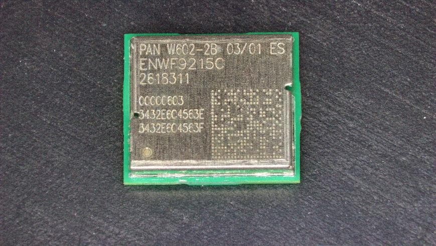
T7V-W602
Jul 14, 2026WiFi / BLE Module
Equipment Class
NII - Unlicensed National Information Infrastructure TX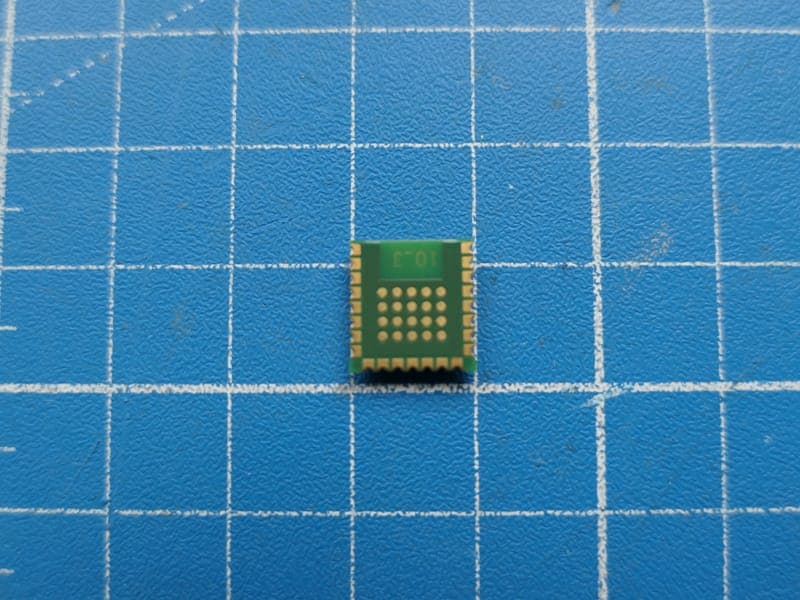
T7V-B611
Dec 19, 2025Bluetooth LE LR Module
Equipment Class
DTS - Digital Transmission System
T7V9019
Apr 18, 2024Wi-Fi 6 Dual Band 2.4 GHz/5 GHz, Bluetooth and 802.15.4 Module
Equipment Class
NII - Unlicensed National Information Infrastructure TX
T7V9520
May 31, 2021Wi-Fi Module
Equipment Class
DTS - Digital Transmission System
T7V301X
Apr 28, 2021Bluetooth Low Energy Module
Equipment Class
DTS - Digital Transmission System