WONSA91004005Badge Tag V2 SA91/004005
Precyse Technologies Inc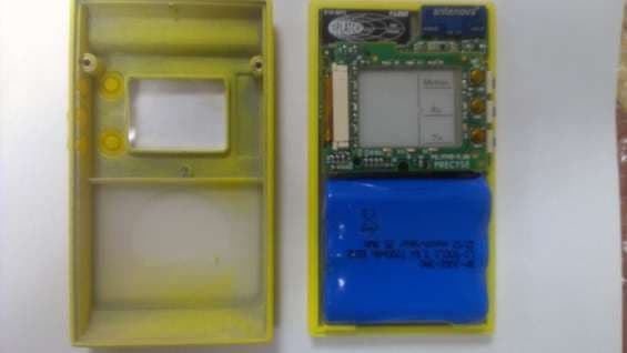
Click to zoom
Application Details
- Equipment Class
- DTS - Digital Transmission System
- Date of Grant
- Mar 20, 2013
- Application Purpose
- Original Equipment
- Date of Application
- Mar 20, 2013
- Equipment Note
- Badge Tag V2 SA91/004005
- Frequency Range
- 905.00000000 - 917.14000000
- Company
- Precyse Technologies Inc
- Country
- Israel
Documents & Files
Document Text
Text extracted from the exhibit documents filed with the FCC. Open a document above to read the original.
Users Manual
Precyse Technologies, Inc. Date: 21 March 2013 Page 1 of 9 Precyse Technologies 100 Ashford Center North Suite 360 Atlanta, GA 30338 Document No.:20121023-1 Revision: 1.2 Badge Tag V2 915MHz User Manual Release Date: 013/230/12 Prepared by: Yossi Nurok Distribution (Check all appropriate): [ ] Precyse Only [ ] Project Team Only [ ] Customer and Supplier Precyse Technologies, Ltd.. Date: 21 March 2013 Page 2 of 9 P.W.Precyse WirelessLtd. Rosh Ha’ayin 48092 Tel: +972 (0)3 9227093 Fax: +972 (0)3 9227515 Revision Record Rev. Effective Date Description 1.0 23/01/13 Badge Tag V2 user manual initial release 1.1 10/03/13 Correction for Frequency range 905-917.14MHz. 1.2 21/03/13 Tag wearing instruction on p.7 Reference documents # Doc # Description 1 Precyse Technologies, Ltd.. Date: 21 March 2013 Page 3 of 9 P.W.Precyse WirelessLtd. Rosh Ha’ayin 48092 Tel: +972 (0)3 9227093 Fax: +972 (0)3 9227515 TABLE OF CONTENTS Section/Title Page Introduction ...................................................................................................... 4 Regulatory Information/disclaimers .................................................................. 4 Product description .......................................................................................... 6 Badge Tag: ................................................................................................... 6 Technical Parameters ...................................................................................... 6 Models: ......................................................................................................... 6 Performance: ................................................................................................ 6 Communication: ............................................................................................ 6 Electrical: ...................................................................................................... 6 Environmental: .............................................................................................. 7 System test configuration ................................................................................. 7 SAT ............................................................................................................... 7 Tag wearing ..................................................................................................... 7 Theory of operation .......................................................................................... 8 iLocate system block diagram .......................................................................... 8 Precyse Technologies, Ltd.. Date: 21 March 2013 Page 4 of 9 P.W.Precyse WirelessLtd. Rosh Ha’ayin 48092 Tel: +972 (0)3 9227093 Fax: +972 (0)3 9227515 Introduction This document provides you with technical support information, and sources for additional product information. Regulatory Information/disclaimers Installation and use of this Wireless Radio device must be in strict accordance with the instructions included in the user documentation provided with the product. Any changes or modifications made to this device that are not expressly approved by the manufacturer may void the user’s authority to operate the equipment. The Manufacturer is not responsible for any radio or television interference caused by unauthorized modification of this device, of the substitution or attachment. Manufacturer and its authorized resellers or distributors will assume no liability for any damage or violation of government regulations arising from failing to comply with these guidelines. This equipment has been tested and found to comply with the limits for a Class B digital device, pursuant to Part 15 of the FCC rules. These limits are designed to provide reasonable protection against harmful interference in a residential installation. This equipment generates, uses, and can radiate radio frequency energy and, if not installed and used in accordance with the instructions, may cause harmful interference to radio communications. This document is confidential and proprietary. No part of this document may be reproduced, stored, or transmitted in any form or by any means without prior written permission from Precyse technologies Inc. This device complies with Part 15 of the FCC Rules. Operation is subject to the following two conditions: (1) This device may not cause harmful interference and (2) This device must accept any interference received, including interference that may cause undesired operation." Precyse Technologies, Ltd.. Date: 21 March 2013 Page 5 of 9 P.W.Precyse WirelessLtd. Rosh Ha’ayin 48092 Tel: +972 (0)3 9227093 Fax: +972 (0)3 9227515 The FCC Wants You to Know This equipment has been tested and found to comply with the limits for a Class B digital device, pursuant to Part 15 of the FCC rules. These limits are designed to provide reasonable protection against harmful interference in a residential installation. This equipment generates, uses and can radiate radio frequency energy and, if not installed and used in accordance with the instructions, may cause harmful interference to radio communications. However, there is no guarantee that interference will not occur in a particular installation. If this equipment does cause harmful interference to radio or television reception, which can be determined by turning the equipment off and on, the user is encouraged to try to correct the interference by one or more of the following measures: a) Reorient or relocate the receiving antenna. b) Increase the separation between the equipment and receiver. c) Connect the equipment to an outlet on a circuit different from that to which the receiver is connected. d) Consult the dealer or an experienced radio/TV technician. FCC Warning Modifications not expressly approved by the manufacturer could void the user authority to operate the equipment under FCC Rules. Precyse Technologies, Ltd.. Date: 21 March 2013 Page 6 of 9 P.W.Precyse W…
Text truncated - open the document above for the full version.
Attestation Statements
Precyse Technologies 100 Ashford Center North Suite 360 Atlanta, GA 30338 attn: Reviewing Engineer Federal Communications Commission 7435 Oakland Mills Road Columbia, MD 21046 To Whom It May Concern: The SA91004005 FCC ID: WONSA91004005 and label is so small that it cannot include the statement specified in FCC Part 15 Sub-part A, Section 15.19 (a) (3) “This device complies with Part 15 of the FCC Rules. Operation is subject to the following two conditions: (1) This device may not cause harmful interference and (2) This device must accept any interference received, including interference that may cause undesired operation." Due to this reason, we are using the provisions of Part 15 Sub-part A, Section 15.19 (a) (5) and this testament appears in a prominent location in the user manual. Please contact me if there is any information you may need. Sincerely, Yossi Nurok HW engineer Precyse Technologies Inc Tel: 972-3-9227107 Mobile: 972-54-4482062 Fax: 972-3-9227515
Block Diagram
CC1101 SWRS061H Page 22 of 98 6 Circuit Description BIAS PA RBIAS XOSC_Q1 XOSC_Q2 CSn SI SO (GDO1) XOSC SCLK LNA 0 90 FREQ SYNTH ADC ADC DEMODULATOR FEC / INTERLEAVER PACKET HANDLER RXFIFO MODULATOR TXFIFO DIGITAL INTERFACE TO MCU RADIO CONTROL RF_P RF_N GDO2 GDO0 (ATEST) RC OSC Figure 9: CC1101 Simplified Block Diagram A simplified block diagram of CC1101 is shown in Figure 9. CC1101 features a low-IF receiver. The received RF signal is amplified by the low-noise amplifier (LNA) and down-converted in quadrature (I and Q) to the intermediate frequency (IF). At IF, the I/Q signals are digitised by the ADCs. Automatic gain control (AGC), fine channel filtering, demodulation, and bit/packet synchronization are performed digitally. The transmitter part of CC1101 is based on direct synthesis of the RF frequency. The frequency synthesizer includes a completely on-chip LC VCO and a 90 degree phase shifter for generating the I and Q LO signals to the down-conversion mixers in receive mode. A crystal is to be connected to XOSC_Q1 and XOSC_Q2. The crystal oscillator generates the reference frequency for the synthesizer, as well as clocks for the ADC and the digital part. A 4-wire SPI serial interface is used for configuration and data buffer access. The digital baseband includes support for channel configuration, packet handling, and data buffering. 7 Application Circuit Only a few external components are required for using the CC1101. The recommended application circuits for CC1101 are shown in Figure 10 and Figure 11. The external components are described in Table 20, and typical values are given in Table 21. The 315 MHz and 433 MHz CC1101EM reference design [1] use inexpensive multi- layer inductors. The 868 MHz and 915 MHz CC1101EM reference design [2] use wire- wound inductors as this give better output power, sensitivity, and attenuation of harmonics compared to using multi-layer inductors. Refer to design note DN032 [24] for information about performance when using wire-wound inductors from different vendors. See also Design Note DN013 [15], which gives the output power and harmonics when using multi-layer inductors. The output power is then typically +10 dBm when operating at 868/915 MHz. 7.1 Bias Resistor The bias resistor R171 is used to set an accurate bias current.
Block Diagram
LNA_OUT PA_IN PA_OUT HGM BIAS PA_EN LNA_EN PREAMP ENEN LNA EN LOGIC BIAS LNA_IN VDD_PA1VDD_LNA TR_SW PA VDD_PA2 CC1190 www.ti.comSWRS089 A –NOVEMBER 2009–REVISED FEBRUARY 2010 850 – 950 MHz RF Front End Check for Samples:CC1190 1 FEATURESAPPLICATIONS • 850 - 950 MHz ISM Bands Wireless Systems • Seamless Interface to Sub-1 GHz Low Power RF Devices from Texas Instruments • Wireless Sensor Networks • Wireless Industrial Systems • Up to 27 dBm (0.5 W) Output Power • IEEE 802.15.4 Systems • 6 dB Typical Sensitivity Improvement with • Wireless Consumer Systems CC11xx and CC430 • Wireless Metering (AMR/AMI) Systems • Few External Components • Smart Grid Wireless Networks – Integrated PA – Integrated LNA DESCRIPTION – Integrated Switches CC1190 is a cost-effective and high-performance RF – Integrated Matching Network Front End for low-power and low-voltage wireless – Integrated Inductors applications at 850 - 950 MHz. • Digital Control of LNA and PA Gain by HGM CC1190 is a range extender for the sub-1 GHz Pin low-power RF transceivers, transmitters, and • 50-nA in Power Down (LNA_EN = PA_EN = 0) System-on-Chip devices from Texas Instruments. • High Transmit Power Efficiency CC1190 integrates a power amplifier (PA), a – PAE = 50% at 26 dBm Output Power low-noise amplifier (LNA), switches, and RF matching for the design of a high-performance wireless • Low Receive Current Consumption systems. – 3 mA for High Gain Mode CC1190 increases the link budget by providing a – 26 μA for Low Gain Mode power amplifier for increased output power, and an • 2.9 dB LNA Noise Figure, Including Switch and LNA with low noise figure for improved receiver External Antenna Match sensitivity. • RoHS Compliant 4-mm × 4-mm QFN-16 CC1190 provides an efficient and easy-to-use range Package extender in a compact 4-mm × 4-mm QFN-16 • 2 V to 3.7 V Operation package. CC1190 BLOCK DIAGRAM 1 Please be aware that an important notice concerning availability, standard warranty, and use in critical applications of Texas Instruments semiconductor products and disclaimers thereto appears at the end of this data sheet. PRODUCTION DATA information is current as of publication date. Copyright © 2009–2010, Texas Instruments Incorporated Products conform to specifications per the terms of the Texas Instruments standard warranty. Production processing does not necessarily include testing of all parameters.
Cover Letter(s)
Precyse Technologies 100 Ashford Center North Suite 360 Atlanta, GA 30338 To Whom It May Concern, We hereby authorize Maurice Dadoun QualiTech Laboratories to act on our behalf regarding the FCC ID Certification Process for the following application: iLocate SA tag Model SA91004005 FCC ID: WONSA91004005 Thank you, Yossi Nurok Hardware engineer Precyse Technologies Tel: 972-3-9227107 Mobile: 972-54-4482062 Fax: 972-3-9227515
Cover Letter(s)
Federal Communications Commission Authorization and Evaluation Division Confidentiality Request regarding application for certification of FCC ID: WONSA91004005. Pursuant to Sections 0.457 and 0.459 of the Commission’s Rules, we hereby request confidential treatment of information accompanying this application as outlined below: SA91004005 BlkDia.pdf SA91004005 schem.pdf SA91004005 Partlist.pdf The above materials contain trade secrets and proprietary information not customarily released to the public. The public disclosure of these materials may be harmful to the applicant and provide unjustified benefits to its competitors. The applicant understands that pursuant to Section 0.457 of the Rules, disclosure of this application and all accompanying documentation will not be made before the date of the Grant for this application. Sincerely, Yossi Nurok Hardware engineer
External Photos
External Photographs - BadgeTag V2 Photograph 1- Front View Precyse Technologies, Inc. Page 2 of 5 BadgeTag V2 EMC Lab Photograph 2 Photograph 3 Precyse Technologies, Inc. Page 3 of 5 BadgeTag V2 EMC Lab Photograph 4 Photograph 5 Precyse Technologies, Inc. Page 4 of 5 BadgeTag V2 EMC Lab Photograph 6 Photograph 7 Precyse Technologies, Inc. Page 5 of 5 BadgeTag V2 EMC Lab Photograph 8
Internal Photos
Internal Photographs - BadgeTag V2 Photograph 1 Precyse Technologies, Inc. Page 2 of 10 BadgeTag V1 Vehicle EMC Lab Photograph 2 Precyse Technologies, Inc. Page 3 of 10 BadgeTag V1 Vehicle EMC Lab Photograph 3 Precyse Technologies, Inc. Page 4 of 10 BadgeTag V1 Vehicle EMC Lab Photograph 4 Precyse Technologies, Inc. Page 5 of 10 BadgeTag V1 Vehicle EMC Lab Photograph 5 Precyse Technologies, Inc. Page 6 of 10 BadgeTag V1 Vehicle EMC Lab Photograph 6 Precyse Technologies, Inc. Page 7 of 10 BadgeTag V1 Vehicle EMC Lab Photograph 7 Precyse Technologies, Inc. Page 8 of 10 BadgeTag V1 Vehicle EMC Lab Photograph 8 Precyse Technologies, Inc. Page 9 of 10 BadgeTag V1 Vehicle EMC Lab Photograph 9 Precyse Technologies, Inc. Page 10 of 10 BadgeTag V1 Vehicle EMC Lab Photograph 10
Operational Description
Badge Tag V2 Description of the EUT system/test Item: Product name: Badge Tag V2 SA9100405 General Description: The SA Tag is used to track assets in real time. It is based on an RF transceiver and a microcontroller. It uses the Precyse N3 proprietary protocol which provides a 2 way, half duplex communication with the base station. The unit is powered by a 3.6V 3xAA battery pack. Specifications: Frequency: 905-917.14MHz ISM license free band Number of Channels: 16 Modulation: 2-FSK Channel bandwidth: 800 KHz EIRP: Up to 17dBm, digitally controlled Communication protocol: N3. Transmission: Event base and on demand External interfaces: 3 user buttons, buzzer, GPS receiver. Internal sensors: Motion, temperature sensors. Antenna Gain: 0 dBi Clock frequencies: Frequency [MHz] Location 26MHz PB_MTRF915-01 32MHz PB_MTMB-A_00 32.768KHz PB_MTMB-A_00 CC1101 Transceiver Data sheet CC1190 PA-LNA Data Sheet
Operational Description
The Badge Tag-V2 device cannot charge the battery pack (see below): A. Diagram of battery pack. The diodes set the current direction only towards unit. B. Picture of the inside of the battery pack.
RF Exposure Info
Badge Tag V2 Product name: Badge Tag V2 SA91004005 Specifications: Frequency: 905-917.14MHz ISM license free band Number of Channels: 16 Modulation: 2-FSK Channel bandwidth: 800 KHz EIRP: Up to 17dBm, digitally controlled Communication protocol: N3. Transmission: Event base and on demand External interfaces: 3 user buttons, buzzer, GPS receiver. Internal sensors: Motion, temperature sensors. Antenna Gain: 0 dBi RF EXPOSURE In compliance with FCC Section 1.1307 (b) (1) for FCC RF exposure: 1. Badge Tag V2 operates in worst case condition with 0.5% duty cycle @ 17dBm peak power, meaning 17dBm+10*log(0.5/100)=-6dBm average power, equivalent to 0.25mW ; this is the source based time averaged maximum conducted power of channel, including tune-up tolerance. 2. The highest operating frequency 917.14GHz and √f(GHz)=0.958 3. The distance between the EUT antenna and human body is 23.7mm, see measurement dY in picture below. 4. SAR test exclusion is based on the following calculation according to the KDB procedure: [(max. power of channel, including tolerance, mW)/ (min. test separation distance, mm)] · [√f (GHz)] ≤ 3.0 for 1-g , [0.25 / 23.7]* √917.14 = 0.011 ≤ 3.0
Test Report
Electromagnetic Compatibility Test Report Test Report No: PCE 310113 Issued on: January 31, 2013 Product Name BadgeTag V2 Tested According to FCC 47 CFR, Part 15.247 Tests Performed for Precyse Technologies, Inc. 11 Amal Street, Afek Industrial Park, P. O. Box 11761, 48092 Rosh Haayin Tel: +972-3-922 7093 QualiTech EMC Laboratory 30 Hasivim Street,P.O.Box 7500 Petah-Tikva, 4951169, Israel Tel: +972-3-926 8443 Fax: +972-3-928 7490 EMC Test Report: PCE 310113 Date: 31.01.2013, Rev.1 Precyse Technologies, Inc. Page 2 of 36 BadgeTag V2 EMC Lab The information contained herein is the property of QualiTech, EMC Lab and is supplied without liability for errors or omissions. The copyright for this document vests in QualiTech, EMC Lab. All rights reserved. This Test Report may not be reproduced, by any method, without the written permission of the QualiTech, EMC Lab. If and when such permission is granted, the report must be reproduced only in the full format. Test Personnel Tests Performed By: ----------------------------------- Sergey Kapustin Report Prepared By: ------------------------------------- Bina Talkar Report Reviewed By: ------------------------------------- Rami Nataf Compliance Engineer & Operation Manager QualiTech EMC Laboratory Report approved By: ------------------------------------- Maurice Dadoun EMC Lab. Manager QualiTech EMC Laboratory EMC Test Report: PCE 310113 Date: 31.01.2013, Rev.1 Precyse Technologies, Inc. Page 3 of 36 BadgeTag V2 EMC Lab Test Report details: Test commencement date: 14.01.2013 Test completion date: 17.01.2013 Customer’s representative: Yossi Nurok Issued on: 31.01.2013 Assessment information: This report contains an assessment of the EUT against Electromagnetic Compatibility based upon tests carried out on the samples submitted. The results contained in this report relate only to the items tested. Manufactured products will not necessarily give identical results due to production and measurement tolerances. QualiTech, EMC Lab does not assume responsibility for any conclusion and generalization drawn from the test results with regards to other specimens or samples of type of the equipment represented by test item. The EUT was set up and exercised using the configuration, modes of operation and arrangements defined in this report only. Modifications: Modifications made to the EUT None Modifications made to the Test Standard None EMC Test Report: PCE 310113 Date: 31.01.2013, Rev.1 Precyse Technologies, Inc. Page 4 of 36 BadgeTag V2 EMC Lab Summary of Compliance Status Test Spec. Clause Test Case Remarks 47 CFR §15.247 (a) (2) 6 dB Bandwidth Comply 47 CFR §15.247 (b) (3) (4) Maximum Conducted (Average) Output Power Comply 47 CFR §15.247 (e) Maximum Power Spectral Density in the Fundamental Emissions Comply 47 CFR §15.247 (d) Unwanted Conducted Emissions into Non-Restricted Bands Comply 47 CFR §15.247 (d), & §15.205, & §15.209(a) Unwanted Radiated Emissions into Restricted Frequency Bands Comply 47 CFR §15.203 Antenna Connector Requirements Comply EMC Test Report: PCE 310113 Date: 31.01.2013, Rev.1 Precyse Technologies, Inc. Page 5 of 36 BadgeTag V2 EMC Lab Table of Contents 1. GENERAL DESCRIPTION .............................................................................................................................. 6 2. METHOD OF MEASUREMENTS .................................................................................................................. 7 2.1. Conducted RF Measurements: ................................................................................................. 7 2.2. Radiated Emission measurements: ........................................................................................... 7 2.3. Worst Case Results: ................................................................................................................... 8 3. TEST FACILITY & UNCERTAINTY OF MEASUREMENT ..................................................................... 9 3.1. Accreditation/ Registration reference: ..................................................................................... 9 3.2. Test Facility description ............................................................................................................ 9 3.3. Uncertainty of Measurement: ................................................................................................... 9 4. BADGETAG V2: REPORT OF MEASUREMENTS AND EXAMINATIONS ......................................... 10 4.1. 6 dB Bandwidth ........................................................................................................................ 10 4.2. Maximum Conducted (Average) Output Power ................................................................... 14 4.3. Maximum Power Spectral Density Level in the Fundamental Emissions .......................... 15 4.4. Unwanted Conducted Emissions into Non-Restricted Frequency Bands ........................... 18 4.5. Unwanted Radiated Emissions into Restricted Frequency Bands ...................................... 26 4.6. Antenna Connector Requirements ......................................................................................... 32 5. APPENDIX ....................................................................................................................................................... 33 EMC Test Report: PCE 310113 Date: 31.01.2013, Rev.1 Precyse Technologies, Inc. Page 6 of 36 BadgeTag V2 EMC Lab 1. General Description Description of the EUT system/test Item: Product name: FCC ID: WONSA91004005 Description: The SA Tag is used to track assets in real time. It is based on an RF transceiver and a microcontroller. It uses the Precyse N3 proprietary protocol which provides a 2 way, half duplex communication with the base station. The unit is powered by a 3.6V 3xAA battery pack. Frequency range: 902 – 928 MHz Type of Modulation: 2-FSK Antenna Gain: 902 – 928 MHz: 0 dBi EMC Test Report: PCE 310113 Date: 31.01.2013, Rev.1 …
Text truncated - open the document above for the full version.
Test Setup Photos
Exhibit - BadgeTag V2 Photograph 1: Radiated Emissions Precyse Technologies, Inc. Page 2 of 2 BadgeTag V2 EMC Lab Photograph 2: Conducted emissions
Contact Information
Applicant
Yossi Nurok(Hardware Engineer)
Technical Contact
Precyse Technologies IncYossi Nurok
[email protected]972-3-922-7107
Ha'amal 11 · Rosh Ha'ayin · Israel
Non-Technical Contact
Precyse Technologies IncReuven Ben Haim
[email protected]972-3-922-7093
Test Firm
QualiTech EMC Laboratory (ECI Telecom)Yossi Zucker
Technical Specifications
| # | Rule Parts | Frequency Range | Power Output |
|---|---|---|---|
| 1 | 15C | 905 MHz - 917.14 MHz | 41.78 mW |
Other Applications from Precyse Technologies Inc
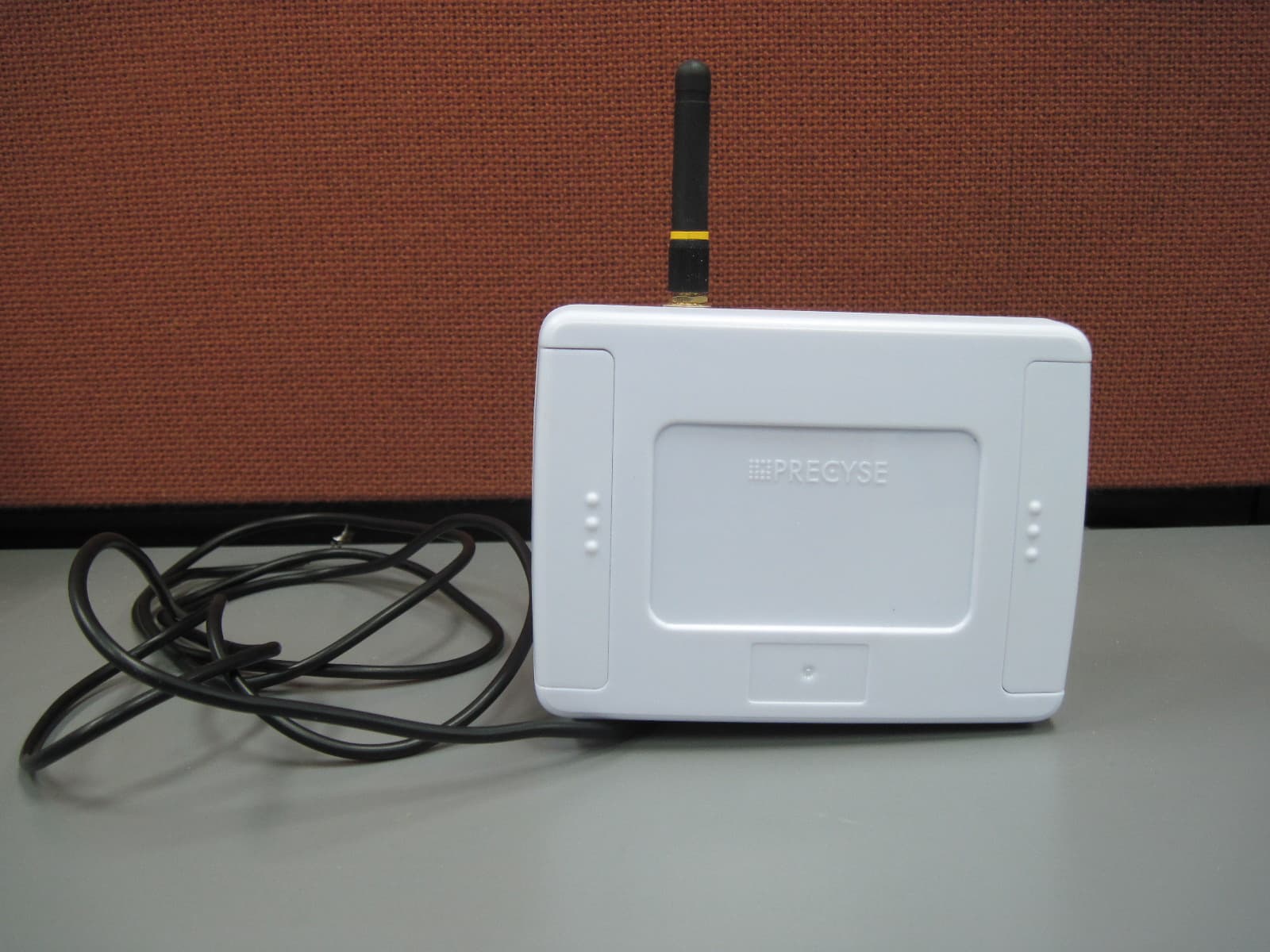
WONBC91005010
Nov 05, 2013915 MICRO BEACON
Equipment Class
DTS - Digital Transmission System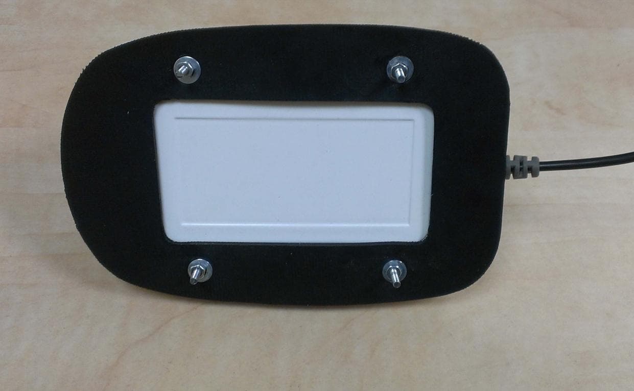
WONSA91004201
Mar 20, 2013Vehicle AGPStag V1 SA91/004201
Equipment Class
DTS - Digital Transmission System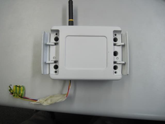
WONBC91005002
Dec 19, 2012MICRO BEACON EQ-55
Equipment Class
DTS - Digital Transmission System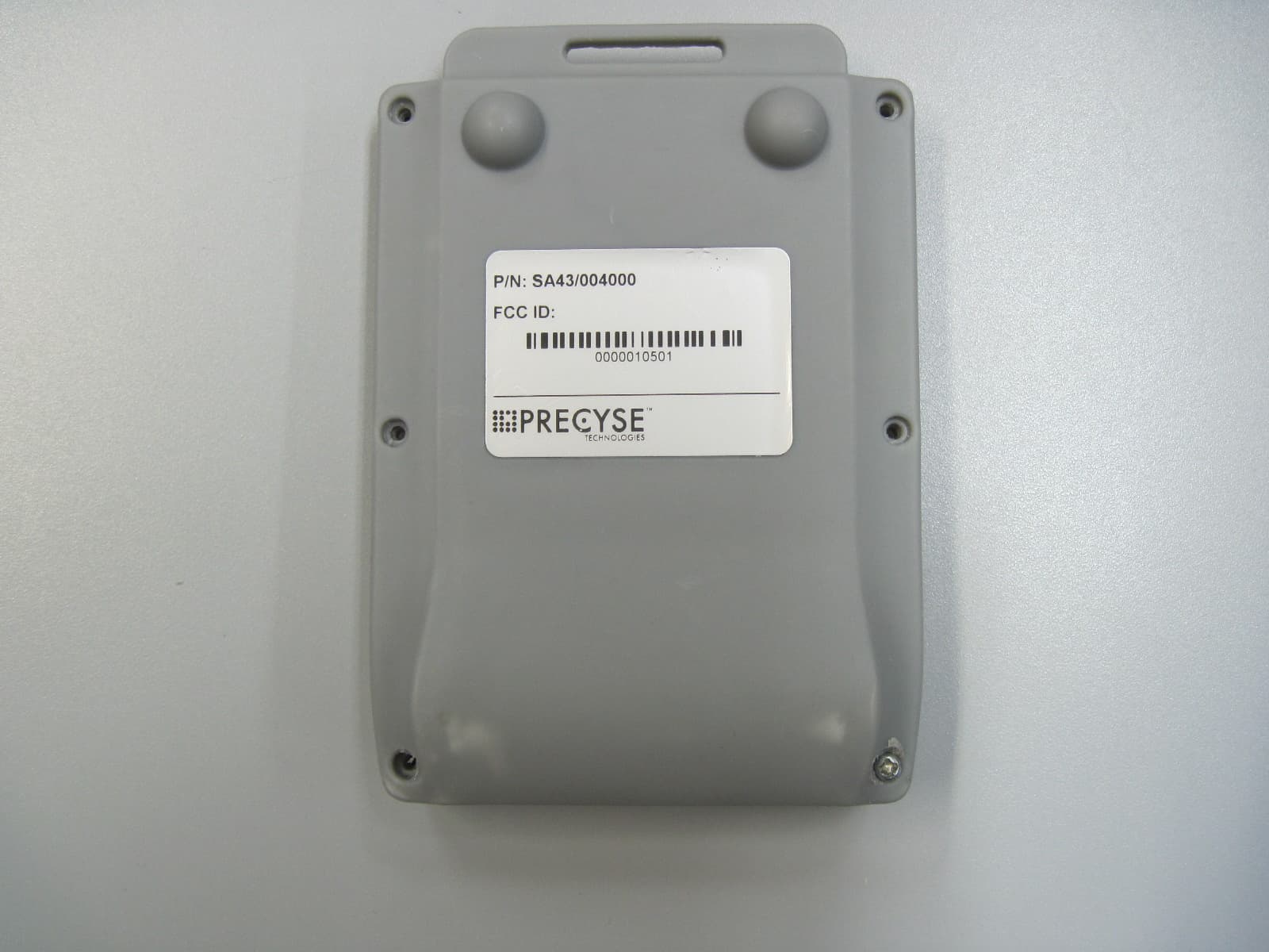
WONSA91004000
Jul 08, 2012SA TAG 915 MHz
Equipment Class
DTS - Digital Transmission System
WONBS91103000
Jun 20, 2012PBS BASE STATION
Equipment Class
DTS - Digital Transmission System