X4D-R4600-2AXCommnunications Control unit
ADLINK TECHNOLOGY INC.
Click to zoom
Application Details
- Equipment Class
- JAD - Part 15 Class A Digital Device
- Date of Grant
- Apr 25, 2021
- Application Purpose
- Original Equipment
- Date of Application
- Apr 25, 2021
- Equipment Note
- Commnunications Control unit
- Company
- ADLINK TECHNOLOGY INC.
- Country
- Taiwan
Documents & Files
Document Text
Text extracted from the exhibit documents filed with the FCC. Open a document above to read the original.
Users Manual
DOC#NCP-R4600 GEN2-SOW Nomad Digital R4600 GEN2 Communications Control Unit User’s Manual DOC#NCP-R4600 GEN2-SOW Revision History Revision Change Date 0.1 Initial version Nov. 2, 2018 DOC#NCP-R4600 GEN2-SOW Contents 1 NDL requirements ..................................................................................................................................... 4 Power ................................................................................................................................................. 4 Expansion ........................................................................................................................................... 5 ECC Memory option ........................................................................................................................... 7 Software ............................................................................................................................................. 7 2 Product Specifications ............................................................................................................................... 9 No CMOS battery - RTC will not maintain date time information ........................................................... 11 3 System Block Diagram ............................................................................................................................. 12 4 Mechanical Drawing reference ............................................................................................................... 13 External chassis drawings and mounting plate ................................................................................ 13 Front panel labelling ........................................................................................................................ 14 5 Internal drawings..................................................................................................................................... 15 Drawing of modem area and PCB designations ............................................................................... 15 Suggested Pigtail routing ................................................................................................................. 16 6 Design Details .......................................................................................................................................... 17 Power ignition control ...................................................................................................................... 17 7 Connector details and Pin out................................................................................................................. 18 External Connectors ......................................................................................................................... 18 External Connectors continued ........................................................................................................ 19 8 Additional data ........................................................................................................................................ 20 DOC#NCP-R4600 GEN2-SOW 1 NDL requirements Power Floating wide range DC input to support EN50155:2017 and ignition input to control system power plus initiate graceful operating system shutdown. The ignition control signal is to be referenced to input supply voltage as requested by NDL and is detailed in Section 2 Product Specifications. A flow diagram is shown under 6.2 power ignition control. A TVS diode is fitted between the plus and minus power inputs, there are no voltage clamping devices between these inputs and the chassis. A standard 1000VAC voltage withstand test with shorted plus – minus is supported. From EN 50155:2017:- 13.4.9.3 Voltage withstand test Nominal battery voltage and/or I/O voltage Test voltage 72 V DC ≤ V DC < 125 V DC or from 50 to 90 V AC rms 1 000 V AC or 1 500 V DC DOC#NCP-R4600 GEN2-SOW Expansion The unit is equipped with four mPCIe slots, two m.2 slots from I/O board and one m.2 slot from the motherboard as detailed in Section 2. Two m.2 slots from the modem area (Section 5.1 location M.2-1 & M.2-2) provide USB 3.0 signaling and one m.2 from the motherboard provides USB3.0 and SATA signaling for a storage device. Two mPCIe slots with USB 3.0 signaling (Section 5.1 mPCIe-3 & mPCIe-4) will be configurable to support isolation of pins 22, 28 and 48 using dipswitches, this is to allow fitment of modems requiring these pins to be left open. Two mPCIe slots with USB 2.0 and PCIe x1 signaling (Section 5.1 mPCIe-5 & mPCIe-6) will follow PCIe mini card spec V1.2. The expansion slot pin outs have been designed to support mPCIe USB3.0 and M.2 USB3.0. Installation of internal m.2 storage slot will require removal of the chassis covers. To help prevent damage to the screw head, a torx fitting will be used Torx type M3, F HEAD, L5 and their locations are shown in the chassis underside view under the mechanical drawings section. Slot Location Signal M.2 I/O board (AFM) USB 3.0 M.2 I/O board (AFM) USB 3.0 mPCIe I/O board (AFM) USB 3.0 mPCIe I/O board (AFM) USB 3.0 mPCIe I/O board (AFM) USB 2.0, PCIe x1 mPCIe I/O board (AFM) USB 2.0, PCIe x1 M.2 Motherboard (MB) S ATA, USB3.0 1.2.1 Pin-out of mini PCIe slots DOC#NCP-R4600 GEN2-SOW Remark: background in amber show the pin difference between MC7445 and LM960 Note : Pin 28 Dip Switch only present on Mass production units Pin # mPCIe slot 5 & 6 USB 2.0+PCIe x1 mPCIe slot 3 & 4 USB 3.0 Sierra MC7455 module Telit LM960 module Notes Location AFM AFM ---- 1 MPCIE_5_WAKE_N Module define WAKE# NC 2 P3V3_SB_MPCIE_5 3V3VCCVBATT 3 NC NCANT_CTRL0/GPIO1GPIO_01 4 GND GNDGNDGND 5 NC NCANT_CTRL1/GPIO2GPIO_02 6 P1V5_MPCIE_5 NCNCNC 7 MPCIE_5_CLKREQ_N NCUSIM2_RSTPCIE_CLKREQ_N* *datasheet r7 Information – PCIe bus is currently NOT supported, PCI pins marked with * are for future use only 8 MODEM_SIM5_VSIM SIM1_PWR USIM_PWR SIMVCC1 9 GND GNDGNDGND 10 MODEM_SIM5_DA…
Text truncated - open the document above for the full version.
External Photos
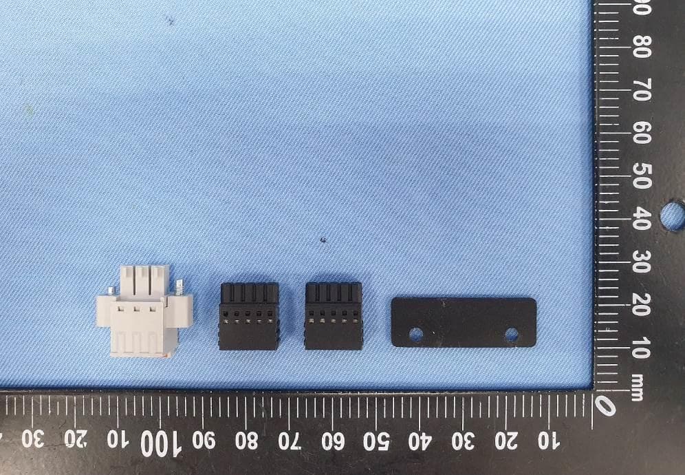
Pa ge: A1-1/ 9 Report No.: T210113D05 Ref No.:T200717D02 Rev.: 02 APPENDIX 1 - PHOTOGRAPHS OF EUT Pa ge: A1-2/ 9 Report No.: T210113D05 Ref No.:T200717D02 Rev.: 02 Pa ge: A1-3/ 9 Report No.: T210113D05 Ref No.:T200717D02 Rev.: 02
Internal Photos
Pa ge: A1-4/ 9 Report No.: T210113D05 Ref No.:T200717D02 Rev.: 02 Pa ge: A1-5/ 9 Report No.: T210113D05 Ref No.:T200717D02 Rev.: 02 Pa ge: A1-6/ 9 Report No.: T210113D05 Ref No.:T200717D02 Rev.: 02 Pa ge: A1-7/ 9 Report No.: T210113D05 Ref No.:T200717D02 Rev.: 02 Pa ge: A1-8/ 9 Report No.: T210113D05 Ref No.:T200717D02 Rev.: 02 Pa ge: A1-9/ 9 Report No.: T210113D05 Ref No.:T200717D02 Rev.: 02
Test Report
Page: 1/ 25 Report No.: T210113D05-D Ref No.:T200717D02-D Rev.: 04 No.163-1, Jhongsheng Rd., Xindian Dist., New Taipei City, Taiwan /新北市新店區中生路163-1號 t: (886-2) 2217-0894 f: (886-2) 2217-1029 www.sgs.com.tw www.ccsrf.com Unless otherwise stated the results shown in this test report refer only to the sample(s) tested and such sample(s) are retained for 90 days only. 除非另有說明,此報告結果僅對測試之樣品負責,同時此樣品僅保留90天。本報告未經本公司書面許可,不可部份複製。 This document is issued by the Company subject to its General Conditions of Service printed overleaf, available on request or accessible at http://www.sgs.com.tw/Terms-and-Conditions and, for electronic format documents, subject to Terms and Conditions for Electronic Documents at http://www.sgs.com.tw/Terms-and-Conditions. Attention is drawn to the limitation of liability, indemnification and jurisdiction issues defined therein. Any holder of this document is advised that information contained hereon reflects the Company’s findings at the time of its intervention only and within the limits of client’s instruction, if any. The Company’s sole responsibility is to its Client and this document does not exonerate parties to a transaction from exercising all their rights and obligations under the transaction documents. This document cannot be reproduced, except in full, without prior written approval of the Company. Any unauthorized alteration, forgery or falsification of the content or appearance of this document is unlawful and offenders may be prosecuted to the fullest extent of the law. Compliance Certification Services Inc. 程智科技股份有限公司 Member of the SGS Group FCC TEST REPORT for Communications Control Unit MODEL: R4600-XXX(X= A~Z, a~z, 0~9) Issued to: ADLINK TECHNOLOGY INC. 9F, No.166, Jian Yi Rd., Zhonghe Dist., New Taipei City, 235 Taiwan Issued by: Compliance Certification Services Inc . Xindian Lab. No.163-1, Jhongsheng Rd., Xindian Dist., New Taipei Cit y, Taiwan. TEL: 886-2-22170894 FAX: 886-2-22171029 Issued Date: April 23, 2021 Note: This document may be altered or revised by Compliance Certification Services Inc. personnel only, and shall be noted in the revision section of the document. The client should not use it to claim product endorsement by TAF, A2LA, NIST or any government agencies. Page: 2/25 Report No.: T210113D05-D Ref No.:T200717D02-D Rev.: 04 Revision History Rev. Issue Date Revisions Effect Pa ge Revised By 00 August 11, 2020 Initial Issue ALL Wendy Wang 01 March 8, 2021 Update ferrite core to internal cable. ALL Wendy Wang 02 April 7, 2021 1. Removed test setup photos, create a new file and mark ferrite core in red. 2. Added “----End of Test Report----" in last page. 3. Revised summary table in page 4: (a) Added 15.107 and 15.109 (b) Removed “ICES-003 Issue 6-2016" (c) Result of the conducted (power Port): “NA” 4. Removed test results of Conducted Emission in page 13. 5. Added test date in page 19~22. 4, 13, 19~22, 23 Wendy Wang 03 April 21, 2021 1. Removed conduction modes. 2. Add note at final Radiation mode. 3. Add conditions of power supplies which is 24VDC / Normal mode at Plots & Result tables. 6, 19~20, 23~24 Wendy Wang 04 April 23, 2021 1. Revised Equipment name from Power Supply to Power Module. 2. Add 110V pretest data and setup photo. 6~7, 13, 21~22 Wendy Wang Page: 3/25 Report No.: T210113D05-D Ref No.:T200717D02-D Rev.: 04 TABLE OF CONTENTS 1 TEST RESULT CERTIFICATION ...................................................................................................... 4 2 EUT DESCRIPTION ........................................................................................................................... 5 3 TEST METHODOLOGY ..................................................................................................................... 6 3.1. DECISION OF FINAL TEST MODE .................................................................................................... 6 3.2. EUT SYSTEM OPERATION ............................................................................................................... 6 4 SETUP OF EQUIPMENT UNDER TEST ........................................................................................... 7 4.1. DESCRIPTION OF SUPPORT UNITS ............................................................................................... 7 4.2. CONFIGURATION OF SYSTEM UNDER TEST ................................................................................ 8 5 FACILITIES AND ACCREDITATIONS ............................................................................................... 9 5.1. FACILITIES ......................................................................................................................................... 9 5.2. ACCREDITATIONS ............................................................................................................................. 9 5.3. MEASUREMENT UNCERTAINTY ...................................................................................................... 9 6 CONDUCTED EMISSION MEASUREMENT .................................................................................. 10 6.1. LIMITS OF CONDUCTED EMISSION MEASUREMENT ................................................................. 10 6.2. TEST INSTRUMENTS ...................................................................................................................... 10 6.3. TEST PROCEDURES ....................................................................................................................... 11 6.4. TEST SETUP .................................................................................................................................... 12 6.5. DATA SAMPLE ................................................................................................................................. 12 6.6. TEST RESULTS ................................................................................................................................ 13 7 RADIATED EMISSION MEASUREMENT ...…
Text truncated - open the document above for the full version.
Test Setup Photos
Pa ge: A1-1/ 3 Report No.: T210113D05 Rev.: 00 RADIATED EMISSION TEST 24VDC / Normal Mode Pa ge: A1-2/ 3 Report No.: T210226D03 Rev.: 00 110VDC / Normal Mode Pa ge: A1-3/ 3 Report No.: T210226D03 Rev.: 00 Ferrite core
Test Setup Photos
Pa ge: A1-1/ 2 Report No.: T210113D05 Rev.: 00 RADIATED EMISSION TEST Pa ge: A1-2/ 2 Report No.: T210226D03 Rev.: 00 Ferrite core
Contact Information
Applicant
Sean Ba(Senior Engineer)
Technical Contact
Compliance Certification Services Inc.Eva Fan
[email protected]886-2-22170894
No.163-1, Jhongsheng Rd., Xindian Dist., · New Taipei City · Taiwan
Non-Technical Contact
Compliance Certification Services Inc.Eva Fan
[email protected]886-2-22170894
Test Firm
Compliance Certification Services Inc.Rick Yeo
Technical Specifications
| # | Rule Parts | Frequency Range | Power Output |
|---|---|---|---|
| 1 | 15B | - | - |
Other Applications from ADLINK TECHNOLOGY INC.
X4D-EMU-200
Nov 09, 2023Arm-based IoT Gateway with WiFi
Equipment Class
NII - Unlicensed National Information Infrastructure TXX4D-SC-1
Jul 28, 2020SYSTEM TABLET CONTROLLER
Equipment Class
DTS - Digital Transmission System
X4D-STC-1505
Nov 16, 2015Smart Touch Computer
Equipment Class
DTS - Digital Transmission System
X4D-IMX-3000
Sep 17, 2014Rugged Handheld Device
Equipment Class
DSS - Part 15 Spread Spectrum Transmitter
X4D-IMX-2000
Apr 15, 2013Rugged Handheld Device
Equipment Class
DSS - Part 15 Spread Spectrum Transmitter