YCP-32WB1MMCH01Bluetooth Low Energy module
STMicroelectronics (Rousset) SAS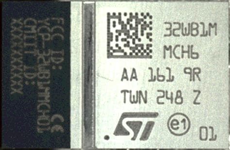
Click to zoom
Application Details
- Equipment Class
- DTS - Digital Transmission System
- Date of Grant
- Jul 17, 2024
- Application Purpose
- Original Equipment
- Date of Application
- Jul 17, 2024
- Equipment Note
- Bluetooth Low Energy module
- Frequency Range
- 2402.00000000 - 2480.00000000
- Country
- France
Documents & Files
Document Text
Text extracted from the exhibit documents filed with the FCC. Open a document above to read the original.
Users Manual
Features •Integrated chip antenna, and option for external antenna • Bluetooth ® Low Energy 5.4 certified •Supports 2 Mbits/s •Frequency band: 2400 to 2483.5 MHz •Advertising extension •TX output power up to +5.5 dBm •RX sensitivity: -96 dBm (1 Mbps) • Dedicated Arm ® Cortex ® -M0+ for radio and security tasks • Dedicated Arm ® Cortex ® -M4 CPU with FPU and ART (adaptative real-time accelerator), up to 64 MHz speed •320-Kbyte flash memory, 48-Kbyte SRAM •Fully integrated BOM, including 32 MHz radio and 32 kHz RTC crystals •Integrated SMPS •Ultra-low power modes for battery longevity •27 GPIOs •SWD, JTAG •Integrated IPD for best-in-class and reliable antenna matching •V DD range: 1.71 to 3.6 V •Temperature range: -40 to 85 °C •Built-in security features, such as secure firmware installation (SFI) for radio stack, PKA, AES 256-bit, RNG, PCROP, CRC, 96-bit UID, possibility to derive 48-bit UEI •Certifications: CE, FCC, ISED, JRF, RoHS, REACH, UKCA •Planned certifications: KC, NCC, SRRC •2-layer PCB Applications •Home automation •Wellness, healthcare, personal trackers •Gaming and toys •Beacons and accessories •Industrial Product status link STM32WB1MMC Bluetooth ® Low Energy 5.4 module STM32WB1MMC Datasheet DS14096 - Rev 4 - January 2024 For further information contact your local STMicroelectronics sales office. www.st.com 1 Introduction This document provides the ordering information and mechanical device characteristics of the STM32WB1MMC module. It must be read in conjunction with DS13258 and RM0473, available on www.st.com. For information on the Arm ® Cortex ® cores, refer to the Cortex ® Technical Reference Manual, available from the www.arm.com website. Note:Arm is a registered trademark of Arm Limited (or its subsidiaries) in the US and/or elsewhere. STM32WB1MMC Introduction DS14096 - Rev 4 page 2/27 2 Description The STM32WB1MMC is an ultralow power, small form factor, certified 2.4 GHz wireless module, supporting Bluetooth ® Low Energy 5.4. Based on the STM32WB15CCY wireless microcontroller, it provides best-in-class RF performance thanks to its good receiver sensitivity and a high output power signal. Its low power features enable extended battery life time, small coin-cell batteries, or energy harvesting. The STM32WB1MMC requires no RF expertise, and is the best way to speed up the application development and to reduce the associated costs. The module is completely protocol stack royalty-free. STM32WB1MMC Description DS14096 - Rev 4 page 3/27 3 Module overview The module is a SiP-LGA77 package (system in package land grid array), based on the proven STM32WB15CCY MCU. The package includes: •LSE and HSE crystals •Passive components for SMPS •Antenna matching and antenna •IPD for RF matching and harmonics rejection Figure 1. Block diagram DT55981 XTAL 32.768 kHz SMPS passive components Power supply filtering IPD Antenna matching STM32WB15CCY 320 KB flash memory 48 KB SRAM XTAL 32 MHz External antenna Communication interfaces RF 3.1 Power supply The power supply requirements are identical to those of the STM32WB1x devices, detailed in the datasheet DS13258. Filtering capacitors on power supply pins and components for the SMPS are already integrated into the module. The SMPS passive components fitted in the module are in configuration-imposing function at 4 MHz, always ON. This is the only available configuration. For additional information on the SMPS, check the reference manual or AN5246, available on www.st.com. 3.2 Clocks As the crystals are already integrated into the package, it is not possible to use any clock in bypass mode. The module integrates a 32.768 kHz crystal for LSE, and a 32 MHz crystal for the HSE clock. •HSE is already tuned. RCC_HSECR.HSETUNE[5:0] value is loaded automatically by hardware. The RCC_HSECR register configuration must not be changed by the user to keep the default parameters. •LSCO and MCO outputs are available. 3.3 Antenna The rectangular module has one shorter side clearly different from the remaining finish surface. This side is unshielded and the mold cover contains the integrated antenna. To use the internal antenna, pins 6 (ANT_INT) and 7 (ANT_EXT) must be connected as in Figure 2. If an external antenna is used, ANT_IN must be shorted to ground, and ANT_OUT connected to the external antenna matching network and to the antenna itself, as in Figure 3. Note:Regulatory certifications obtained by ST apply only to the module with its internal antenna. Designs with external antennas require new certifications. STM32WB1MMC Module overview DS14096 - Rev 4 page 4/27 Figure 2. Connections when using the internal antenna Figure 3. Connections when using an external antenna 3.4 OTP The STM32WB1MMC features a 1-Kbyte one time programmable (OTP) memory for use by the end product (see DS13258 and RM0473). Note:The device uses the first and last words of this area for trimming and identification purposes. As a consequence, addresses 0x1FFF7000h to 0x1FFF7007h and 0x1FFF73F8h to 0x1FFF73FFh cannot be changed. STM32WB1MMC Module overview DS14096 - Rev 4 page 5/27 4 Available peripherals All the peripherals available in STM32WB series microcontrollers based on the WLCSP49 package are available and accessible on this module. The pins on the module offer access to the following system peripherals: •1× DMA controllers (seven channels each) supporting ADC, SPI, I2C, USART, AES, timers •1× USART (ISO 7816, IrDA, SPI master, Modbus and Smartcard mode) •1× LPUART (low power) •SPI running at 32 Mbit/s •I²C (SMBus/PMBus ® ) •1× touch sensing controller, up to 8 sensors •1× 16-bit, four-channel advanced timer •2× 16-bit, two-channel timers •1× 32-bit, four-channel timer •2× 16-bit ultra-low power timers •1× independent SysTick •1× independent watchdog •1× window watchdog. The full pin description is available in DS13258. STM32WB1MMC Available peripherals DS14096 - Rev 4 page 6/27 5 Pin description Figure 4 shows the module pinout package bottom view. Figure 4. STM32WB1MMC …
Text truncated - open the document above for the full version.
Attestation Statements
CERTIFICATION DESIGNATING A U.S. AGENT FOR SERVICE OF PROCESS Date: June 6th, 2024 Federal Communications Commission Authorization and Evaluation Division 7435 Oakland Mills Road Columbia, Maryland 21046 FCC ID: YCP-32WB1MMCH01 To Whom It May Concern: As required by section 2.911(d)(7), we, STMICROELECTRONICS (Rousset) SAS, FRN 0019756717 certify that we acknowledge the designation of a contact located in the United States for purposes of acting as the applicant’s agent for service of process. We, STMICROELECTRONICS (Rousset) SAS, accept to maintain an agent for no less than one year after the grantee has terminated all marketing and importation or the conclusion of any Commission-related proceeding involving the equipment. As required by section 2.911(d)(7), we, STMicroelectronics Inc, address 200 Summit Drive | Suite 405 | Burlington, MA 01803 | USA, FRN: 0033628546] certify that we acknowledge our obligation acting as the applicant’s agent for service of process for the above referenced FCC ID. Thank you for your attention to this matter. Sincerely yours, Signature by applicant: Signature by designated agent (if different from applicant): Printed Name: Pascal Scafidi Printed Name: Francesco Doddo Company: STMicroelectronics (Rousset) SAS Address: 190 Avenue Celestin Coq 13790 Rousset France Company: STMicroelectronics Inc Address: 200 Summit Drive Suite 405 Burlington MA 01803 USA FRN: 0019756717 FRN: 0033628546 Job Title:MDRF Group VP Quality & Reliability Job Title: AME AMS Sensors to Cloud Applications | Director Email: [email protected] Email: [email protected] Telephone: +33 4 76 58 50 00 Telephone: +1 781 472 9634
Attestation Statements
CERTIFICATIONS CONCERNING “COVERED” EQUIPMENT Date: June 6 th , 2024 Federal Communications Commission Authorization and Evaluation Division 7435 Oakland Mills Road Columbia, Maryland 21046 FCC ID: YCP-32WB1MMCH01 To Whom It May Concern: As required by section 2.911(d)(5)(i), STMICROELECTRONICS (ROUSSET) SAS, FRN 0019756717 (“the applicant”) certifies that the equipment for which authorization is sought is not “covered” equipment prohibited from receiving an equipment authorization pursuant to section 2.903 of the FCC rules. As required by section 2.911(d)(5)(ii), STMICROELECTRONICS (ROUSSET) SAS, FRN 0019756717 (“the applicant”) certifies that, as of the date of the filing of the application, the applicant is not identified on the Covered List (as a specifically named entity or any of its subsidiaries or affiliates) as an entity producing “covered” equipment. Thank you for your attention to this matter. Sincerely yours, Signature: Printed Name: Pascal Scafidi Company: STMICROELECTRONICS (ROUSSET) SAS Job Title: MDRF Group VP Quality & Reliability Email: [email protected] Telephone: +33 4 76 58 50 00
Block Diagram
LCIE SUD EST Site de Grenoble Z.I. Centr’Alp 170, Rue de Chatagnon 38430 MOIRANS - FRANCE Page 1/1 BLOCK DIAGRAM AND CLOCK LIST OF EQUIPMENT FCCID: YCP-32WB1MMCH01
Cover Letter(s)
Page 1/1 To: Timco Engineering, Inc 849 NW State Road 45 Newberry, Florida 32669 - United States September 13, 2023 Re: ID Label Location information FCC ID: YCP-32WB1MMCH01 IC: 8976A-32WB1MMCH01 Dear Examiner, We are asking for the permission from “STMicroelectronics SAS.” to place the label for the product into the user manual and package instead of the exterior of the device, due to the dimensions of the “Wireless module” being extremely small. Brand Name: STMicroelectronics (Rousset) SAS Product name: STM32WB1MMC Model name: STM32WB1MMC FCC ID: YCP-32WB1MMCH01 IC: 8976A-32WB1MMCH01 HVIN: STM32WB1MMC If you have any questions, feel free to contact us. Regards, Responsible: Pascal Scafidi Title: MDG Group VP Quality & Reliability Signature:
Cover Letter(s)
Date: July 16, 2024 Federal Communications Commission Authorization and Evaluation Division 7435 Oakland Mills Road Columbia, MD 21046-1609 SUBJECT: Test report complies with 47 CFR PART 15.247 FCC ID: YCP-32WB1MMCH01 Brand/Trade Name: STMICROELECTRONICS SAS Model Number: 32WB1MMCH01 We, STMICROELECTRONICS SAS, hereby declare that our end product, STMICROELECTRONICS SAS, includes 32WB1MMCH01 as listed above. The testing data complies with 47 CFR PART 15.247. Although the product was tested 13 months ago, neither the hardware nor the software has been modified by the manufacturer. Should you have any question, feel free to contact me directly. Sincerely yours, ----------------------------------- Printed Name: Pascal Scafidi Company: STMICROELECTRONICS (ROUSSET) SAS Job Title: MDG Group VP Quality & Reliability Email: [email protected] Telephone: +33 4 76 58 50 00
Cover Letter(s)
MODULAR APPROVAL Attestation letter September 5th, 2023 Timco Engineering, Inc 849 NW State Road 45 Newberry, Florida 32669 - United States Re: Modular Approval attestation letter FCC ID: YCP- 32WB1MMCH01 IC: 8976A- 32WB1MMCH01 Gentlemen, The module STM32WB1MMC meets the requirements for modular approval as detailed in FCC Public notice 15.212 and IC RSS requirements. Compliance to each of the requirements is described below. Clauses Manufacturer’s arguments Modular Approval 15.212 (a)(1)(i) Shielding The module has a metal shield over the radio elements 15.212 (a)(1)(ii) Buffered Data/Modulation STM32WB1MMC is compliant with this rule. 15.212 (a)(1)(iii) Power supply regulation STM32WB1MMC is compliant with this rule 15.212 (a)(1)(iv) Antenna The antenna is permanently attached to the STM32WB1MMC inside the substrate. 15.212 (a)(1)(v) Stand-alone configuration The STM32WB1MMC was tested in a stand-alone configuration, see “Test setup photos” document. 15.212 (a)(1)(vi) Label See “Label” document and exhibition label sample 15.212 (a)(1)(vii) Operating The STM32WB1MMC is compliant with all applicable FCC and IC rules. Details for maintaining compliance are given in the “Datasheet”. 15.212 (a)(1)(viii) RF Exposure The STM32WB1MMC is compliant with all applicable RF exposure requirements. See “RF exposure” document. Please contact me if you have any further question. Best regards, Responsible: Pascal Scafidi Title: MDG Group VP Quality & Reliability Signature:
Cover Letter(s)
Administrative Contact/Manufacturer Company Name STMICROELECTRONICS (Rousset) SAS Address: 190 Avenue Celestin Coq Postcode/Zip Code 13790 City Rousset Country France E-mail Address: [email protected] Date: June 6 th 2024 Letter of Authorization To Whom It May Concern. The undersigned STMicroelectronics (Rousset) SAS (the “Company”), hereby authorizes: Majid MOURZAGH, LCIE SUD EST to represent the Company in the carrying-out of all matters and processes needed for the FCC certification approval equipment authorization for the following products: Trademark STMICROELECTRONICS Manufacturer STMICROELECTRONICS (ROUSSET) SAS Model STM32WB1MMC The authorization granted hereunder shall remain effective until (i) it is either expressly revoked on behalf of the Company or (ii) the beneficiary of this authorization significantly changes his business collaboration or other capacity in relation to the Company as existing on the date of this document, including the cessation of business. The express provisions of this letter set forth the entire authorization granted to the beneficiaries appointed above, and this document revokes and supersedes any prior authorizations by the undersigned within the scope of the authorization granted hereunder. This authorization was executed on June 6 th 2024. On behalf of STMICROELECTRONICS (ROUSSET) SAS Date: 6 June 2024 City: Rousset, France Name: Pascal SCAFIDI Function: MDRF Group VP Quality & Reliability Telephone number: +33 4 76 58 50 00 Email address: [email protected] Signature:
External Photos
LCIE SUD EST Laboratoire de Moirans Z.I. Centr’Alp 170, Rue de Chatagnon 38430 MOIRANS – France Page 1/1 EXTERNAL PHOTOS OF EQUIPMENT FCCID: YCP-32WB1MMCH01
ID Label/Location Info
LCIE SUD EST Laboratoire de Moirans Z.I. Centr’Alp 170, Rue de Chatagnon 38430 MOIRANS - FRANCE Page 1/1 PRODUCT LABELING FCCID: YCP-32WB1MMCH01
Internal Photos
LCIE SUD EST Laboratoire de Moirans Z.I. Centr’Alp 170, Rue de Chatagnon 38430 MOIRANS – France Page 1/1 INTERNAL PHOTOS OF EQUIPMENT FCCID: YCP-32WB1MMCH01 RF Antenna
Operational Description
LCIE SUD EST Laboratoire de Moirans Z.I. Centr’Alp 170, Rue de Chatagnon 38430 MOIRANS - FRANCE GENERAL INFORMATION FCCID: YCP-32WB1MMCH01 1.1. Product description LCIE SUD EST Laboratoire de Moirans Z.I. Centr’Alp 170, Rue de Chatagnon 38430 MOIRANS - FRANCE 1.2. Tested System Details 1.3. Test Methodology Both conducted and radiated testing were performed according to the procedures in ANSI C63.4 or/and ANSI C63.10, FCC Part 15 SubPart 15C. Radiated testing was performed at an antenna to EUT distance of 10 meters. During testing, all equipment’s and cables were moved relative to each other in order to identify the worst case set-up. 1.4. Test facility Tests have been performed: February 13, 2023 to February 14, 2023 This test facility has been fully described in a report and accepted by FCC as compliant with the radiated and AC line conducted test site criteria in ANSI C63.4 or/and ANSI C63.10. This test facility has also been accredited by COFRAC (French accreditation authority for European Union test lab accreditation organization) according to NF EN ISO/IEC 17025, as compliant with test site criteria and competence in 47 CFR Part 15/ANSI C63.4 and EN55032/CISPR32 norms for 89/336/EEC European EMC Directive application. All pertinent data for this test facility remains unchanged.
RF Exposure Info
LCIE SUD EST Laboratoire de Moirans Z.I. Centr’Alp 170, Rue de Chatagnon 38430 MOIRANS – FRANCE RF Exposure Considerations for FCC ID: YCP-32WB1MMCH01 Per FCC KDB 447498 D01 General RF Exposure Guidance v06 The 1-g and 10-g SAR test exclusion thresholds for 100 MHz to 6 GHz are based on source-based time-averaged maximum conducted output power of the RF channel requiring evaluation, adjusted for tune-up tolerance, and the minimum test separation distance required for the exposure conditions. The minimum test separation distance defined in 4.1 f) is determined by the smallest distance from the antenna and radiating structures or outer surface of the device, according to the host form factor, exposure conditions and platform requirements, to any part of the body or extremity of a user or bystander. Minimum test separation distance: 5 mm Step a) For 100 MHz to 6 GHz and test separation distances ≤ 50 mm The 1-g and 10-g SAR test exclusion thresholds are determined by the following: (max푝표푤푒푟표푓 푐ℎ푎푛푛푒푙 ( 푚푊 ) ) (min푡푒푠푡푠푒푝푎푟푎푡푖표푛 푑푖푠푡푎푛푐푒 ( 푚푚 ) ) × √ 푓 ( 퐺퐻푧 ) ≤3.0 푓표푟 1−푔 푆퐴푅 표푟 ≤7.5 푓표푟 10−푔 푒푥푡푟푒푚푖푡푦 푆퐴푅 Where: ▪ f(GHz) is the RF channel transmit frequency in GHz ▪ Power and distance are rounded to the nearest mW and mm before calculation31 ▪ The result is rounded to one decimal place for comparison ▪ The values 3.0 and 7.5 are referred to as numeric thresholds in step b) below The test exclusions are applicable only when the minimum test separation distance is ≤ 50 mm, and for transmission frequencies between 100 MHz and 6 GHz. When the minimum test separation distance is < 5 mm, a distance of 5 mm is applied to determine SAR test exclusion. (dBm) (mW) Min 2.402 5.40 3.47 5 1.07 3 7.5 Exempt from SAR Mid 2.440 5.30 3.39 5 1.06 3 7.5 Exempt from SAR Max 2.480 5.19 3.30 5 1.04 3 7.5 Exempt from SAR Limit for 10-g extremity SAR Verdict Maximum source-based time averaged conducted output power or EIRP (worst case) including tune-up tolerance Channel Frequency (GHz) Minimum separation distance (mm) Result of Eq. 1 Limit for 1-g SAR Conclusion: Therefore our device complies with FCC’s RF radiation exposure limits for general population without SAR evaluation.
Schematics
6 Schematics Figure 5. Reference board schematics DS14096 - Rev 4 page 10/27 STM32WB1MMC Schematics
Test Report
5F., No. 83, Kewang Rd., Longtan Dist., Taoyuan City 32556, Taiwan (R.O.C.) Tel: 886-3-4072728焋Fax: 886-3-4072738 焋[email protected] 1 © Unictron Technologies Corp . All specifications subject to change without notice. www.sanav.com www.unictron.com Product Name: WiFi/Bluetooth Chip Antenna – CW201 Part Number: H2U34C1H1B0100 Features: z Supporting WiFi/Bluetooth, covering 2400 to 2484 MHz z Surface Mount z Dimensions: 2.0 x 1.2 x 0.6 mm z High performance, small size. z RoHS & REACH Compliant Applications: z ISM 2.4 GHz applications z ZigBee/BLE applications z Bluetooth earphone systems z Hand-held devices when WiFi / Bluetooth functions are needed, e.g., Smart phones z IEEE802.11 b/g/n z Wireless PCMCIA cards or USB dongles 5F., No. 83, Kewang Rd., Longtan Dist., Taoyuan City 32556, Taiwan (R.O.C.) Tel: 886-3-4072728焋Fax: 886-3-4072738 焋[email protected] 2 © Unictron Technologies Corp . All specifications subject to change without notice. www.sanav.com www.unictron.com WiFi/Bluetooth Chip Antenna MODEL: CW201 Version: A I. Specifications: Mechanical Specifications Dimensions (mm) 2.0(L) x 1.2 (W) x 0.6 (H) Material Ceramic Termination Ag (environmental Pb free) Environmental Conditions Operation Temperature ( o C) -40 ~ +85 Storage Temperature ( o C) -5 ~ +40 Relative Humidity 10 ~ 70 % Items Specifications Frequencies (MHz) 2400~2484 Efficiency (%) 59.2 Average Gain (dB) -2.3 Peak Gain (dBi) 1.9 Test Condition 40 x 20 mm² (Evaluation board) Impedance (ƻ) 50 Polarization Linear Polarization 5F., No. 83, Kewang Rd., Longtan Dist., Taoyuan City 32556, Taiwan (R.O.C.) Tel: 886-3-4072728焋Fax: 886-3-4072738 焋[email protected] 3 © Unictron Technologies Corp . All specifications subject to change without notice. www.sanav.com www.unictron.com II. Layout Guide: Solder Land Pattern: The solder land pattern (gold marking areas) is shown below. Recommendation on matching circuit will be provided according to customer’s installation conditions. Grounding Pin Signal Input Transmission Line with 50ƻ Impedance Characteristic Top View Bottom View 5F., No. 83, Kewang Rd., Longtan Dist., Taoyuan City 32556, Taiwan (R.O.C.) Tel: 886-3-4072728焋Fax: 886-3-4072738 焋[email protected] 4 © Unictron Technologies Corp . All specifications subject to change without notice. www.sanav.com www.unictron.com III. Mechanical Dimensions: a) Antenna Dimensions b) PIN Definition PIN 1 2 Soldering Pad Signal Input Tuning/Signal Output TOP View Bottom View Side View Unit: mm Unit: mm 5F., No. 83, Kewang Rd., Longtan Dist., Taoyuan City 32556, Taiwan (R.O.C.) Tel: 886-3-4072728焋Fax: 886-3-4072738 焋[email protected] 5 © Unictron Technologies Corp . All specifications subject to change without notice. www.sanav.com www.unictron.com c) Test Board with Antenna Unit: mm 5F., No. 83, Kewang Rd., Longtan Dist., Taoyuan City 32556, Taiwan (R.O.C.) Tel: 886-3-4072728焋Fax: 886-3-4072738 焋[email protected] 6 © Unictron Technologies Corp . All specifications subject to change without notice. www.sanav.com www.unictron.com IV. Properties: a) Return loss (dB) b) Efficiency (%) 5F., No. 83, Kewang Rd., Longtan Dist., Taoyuan City 32556, Taiwan (R.O.C.) Tel: 886-3-4072728焋Fax: 886-3-4072738 焋[email protected] 7 © Unictron Technologies Corp . All specifications subject to change without notice. www.sanav.com www.unictron.com c) Average Gain (dB) d) Peak Gain (dBi) 5F., No. 83, Kewang Rd., Longtan Dist., Taoyuan City 32556, Taiwan (R.O.C.) Tel: 886-3-4072728焋Fax: 886-3-4072738 焋[email protected] 8 © Unictron Technologies Corp . All specifications subject to change without notice. www.sanav.com www.unictron.com V. Antenna Radiation Pattern Measurement: The antenna radiation patterns are measured in Unictron’s 3D Anechoic Chamber. The measurement setup is as show below. Z Y X 5F., No. 83, Kewang Rd., Longtan Dist., Taoyuan City 32556, Taiwan (R.O.C.) Tel: 886-3-4072728焋Fax: 886-3-4072738 焋[email protected] 9 © Unictron Technologies Corp . All specifications subject to change without notice. www.sanav.com www.unictron.com 3D Radiation Gain Pattern 2450 MHz (unit: dBi) X Y Z 5F., No. 83, Kewang Rd., Longtan Dist., Taoyuan City 32556, Taiwan (R.O.C.) Tel: 886-3-4072728焋Fax: 886-3-4072738 焋[email protected] 10 © Unictron Technologies Corp . All specifications subject to change without notice. www.sanav.com www.unictron.com VI. Frequency tuning: System Matching Circuit Component Location Description Vendor Tolerance 1 N/C - - 2 5.0 pF (0402) MURATA ±0.05 pF 3 0.8 pF (0402) MURATA ±0.05 pF 4 2.7 pF (0201) MURATA ±0.05 pF DC Block 22 pF (0402) MURATA ±5% 1 3 2 DC Block 4 5F., No. 83, Kewang Rd., Longtan Dist., Taoyuan City 32556, Taiwan (R.O.C.) Tel: 886-3-4072728焋Fax: 886-3-4072738 焋[email protected] 11 © Unictron Technologies Corp . All specifications subject to change without notice. www.sanav.com www.unictron.com VII. Soldering conditions: Typical Soldering Profile for Lead-free Process VIII. Reminders for use of Unictron’s ceramic chip antennas: a) This chip antenna is made of ceramic materials which is relatively more rigid and brittle compared to circuit board materials. Furthermore, the length of this antenna is quite long. Bending of circuit board at the locations where chip antenna is mounted may cause the cracking of solder joints or antenna itself. b) Punching/cutting of the break-off tab of PCB panel may cause severe bending of the circuit board which may result in cracking of solder joints or chip antenna itself. Therefore break-off tab shall be located away from the installation site of chip antenna. c) Be cautious when ultrasonic welding process needs to be used near the locations where chip antennas are installed. Strong ultrasonic vibration may cause the cracking of chip antenna solder joints. 5F., No. 83, Kewang Rd., Longtan Dist., Taoyuan City 32556, Taiwan (R.O.C.) Tel: 886-3-4072728焋Fax: 886-3-4072738 焋[email protected] 12 © Unictron Technologies Corp . All specifications subject to change with…
Text truncated - open the document above for the full version.
Test Setup Photos
LCIE SUD EST Laboratoire de Moirans Z.I. Centr’Alp 170, Rue de Chatagnon 38430 MOIRANS - FRANCE Page 1/3 CONDUCTED AND RADIATED MEASUREMENT PHOTO FCCID: YCP-32WB1MMCH01 1.1 Conducted emission LCIE SUD EST Laboratoire de Moirans Z.I. Centr’Alp 170, Rue de Chatagnon 38430 MOIRANS - FRANCE Page 2/3 1.2 Radiated emissions LCIE SUD EST Laboratoire de Moirans Z.I. Centr’Alp 170, Rue de Chatagnon 38430 MOIRANS - FRANCE Page 3/3
Contact Information
Applicant
PASCAL SCAFIDI(MDG Group VP Quality & Reliability)
Test Firm
LCIE Etablissement Sud EstAnthony MERLIN
[email protected]0033 4 76 07 36 35
Technical Specifications
| # | Rule Parts | Frequency Range | Power Output |
|---|---|---|---|
| 1 | 15C | 2.40 GHz - 2.48 GHz | 3.47 mW |
Other Applications from STMicroelectronics (Rousset) SAS
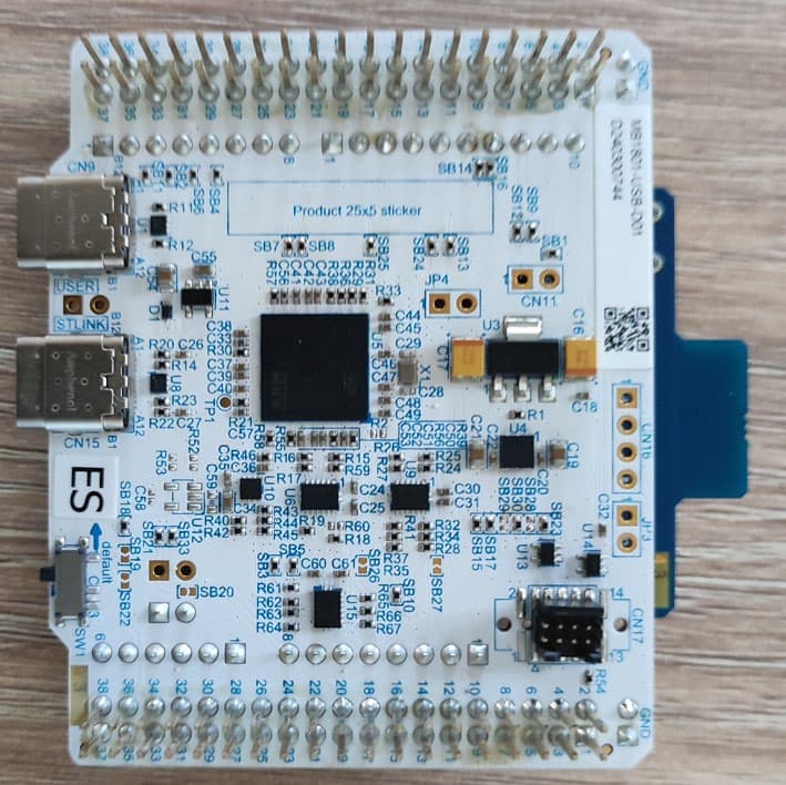
YCP-MB229300
Jun 08, 2026BLE RF evaluation board
Equipment Class
DTS - Digital Transmission System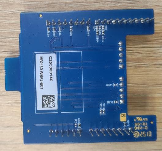
YCP-MB229301
Jun 08, 2026BLE RF evaluation board
Equipment Class
DTS - Digital Transmission System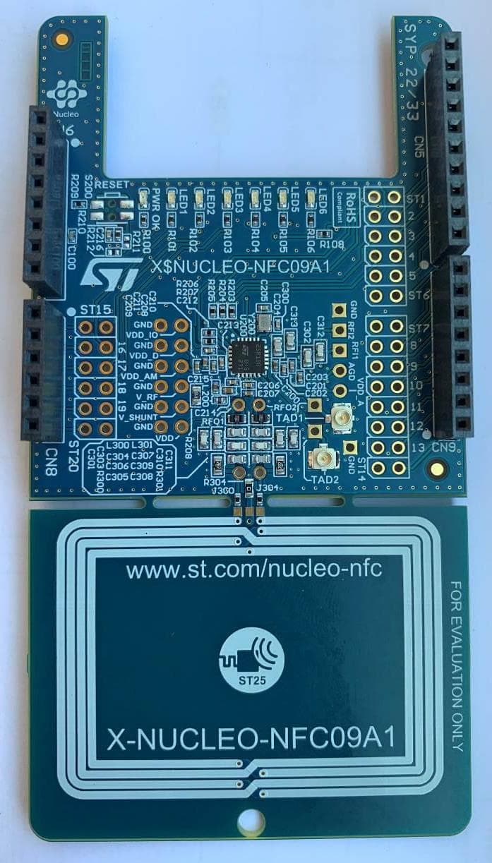
YCPNFC09A1
Oct 01, 2024NFC card reader evaluation board
Equipment Class
DXX - Part 15 Low Power Communication Device Transmitter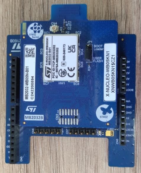
YCP-MB203202
Sep 10, 2024X-NUCLEO-WB05KN1
Equipment Class
DTS - Digital Transmission System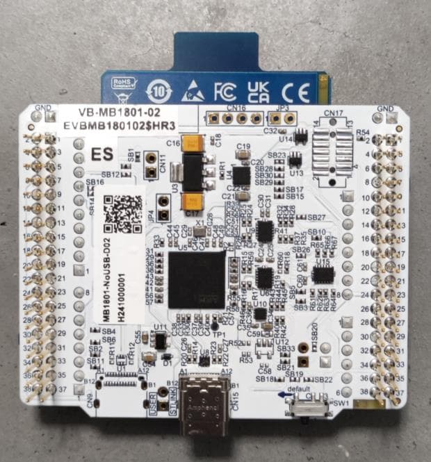
YCP-MB203200
Sep 05, 2024NUCLEO-WB05KZ
Equipment Class
DTS - Digital Transmission System