YCP-MB229301BLE RF evaluation board
STMicroelectronics (Rousset) SAS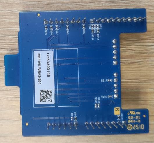
Click to zoom
Application Details
- Equipment Class
- DTS - Digital Transmission System
- Date of Grant
- Jun 08, 2026
- Application Purpose
- Original Equipment
- Equipment Note
- BLE RF evaluation board
- Frequency Range
- 2402.00000000 - 2480.00000000
- Country
- France
Documents & Files
Document Text
Text extracted from the exhibit documents filed with the FCC. Open a document above to read the original.
Users Manual
Introduction The X-NUCLEO-WBA25A1 ARDUINO ® interface board provides Bluetooth ® LE connectivity for developer applications and can be plugged into an STM32 Nucleo board, such as NUCLEO-U385RG-Q, using the ARDUINO ® Uno V3 connectors. The ARDUINO ® interface board features the Bluetooth ® v6.0-compliant and FCC-certified STM32WBA25CE SoC. This device manages the complete Bluetooth ® LE stack and protocols using its Arm ® Cortex ® -M33 core and programmable flash memory. X-NUCLEO-WBA25A1 uses the universal asynchronous receiver transmitter (UART) interface to communicate with the STM32 Nucleo board. It supports operations with or without hardware flow control. A full-duplex serial peripheral interface (SPI) with an interrupt line is also available. The firmware loaded on the module determines the host interface. To change the interface, update the firmware without modifying the hardware. Figure 1. X-NUCLEO-WBA25A1 global view DT80262V1 Picture is not contractual. Bluetooth ® LE expansion board based on the STM32WBA25CE MCU for STM32 Nucleo boards DRAFT UM3608 User manual UM3608 - Rev 1 - January 2026 For further information, contact your local STMicroelectronics sales office. www.st.com 1 Typical application The X-NUCLEO-WBA25A1 expansion board can be used for the evaluation of the STM32WBA25CE device in many applications, such as: •Point‑to‑point communication •Sensor application •Home automation and lighting •Direct test mode (DTM) DRAFT UM3608 Typical application UM3608 - Rev 1 page 2/25 2 Features •Bluetooth ® v6.0 compliant expansion board based on the STM32WBA25CE MCU and featuring preloaded network coprocessor firmware with a UART interface •Embedded MLPF-WB-04D3 impedance matching network and harmonics filter •On-board PCB antenna •Optional SPI through dedicated firmware •ARDUINO ® Uno V3 expansion connector •Compatible with STM32 Nucleo boards •Scalable solution, capable of cascading multiple boards for larger systems •Free comprehensive development firmware library and examples, compatible with the X-CUBE-WBA expansion software package for STM32Cube Note:Arm and Cortex are registered trademarks of Arm Limited (or its subsidiaries or its affiliates) in the US and/or elsewhere. The Arm word and logo are trademarks of Arm Limited (or its subsidiaries) in the US and/or elsewhere. All rights reserved. Note: For information on Bluetooth ® , refer to the www.bluetooth.com website DRAFT UM3608 Features UM3608 - Rev 1 page 3/25 3 Ordering information To order the X-NUCLEO-WBA25A1 expansion board, refer to Table 1. Additional information is available from the datasheet and reference manual of the target STM32. Table 1. Ordering information Order codeBoard referencesTarget STM32 X-NUCLEO-WBA25A1 •MB2160 (1) •MB2293 (2) STM32WBA25CE 1. ARDUINO ® interface board 2.MCU RF board 3.1 Codification The meaning of the codification is explained in Table 2. Table 2. Codification explanation X-NUCLEO-XXXYYZTDescriptionExample: X-NUCLEO-WBA25A1 X-NUCLEOType of boardSTM32 Nucleo expansion board XXXSTM32 MCU seriesSTM32WBA series YYMCU product line in the seriesSTM32WBA25 product line Z Type of connector: •A for ARDUINO ® ARDUINO ® TIndex First generation of Bluetooth ® LE expansion boards based on the STM32WBA25CE MCU for STM32 Nucleo boards DRAFT UM3608 Ordering information UM3608 - Rev 1 page 4/25 4 Conventions Table 3. Conventions for solder bridges ConventionDefinition Solder bridge SBx ONSBx connections closed by 0 Ω resistor Solder bridge SBx OFFSBx connections left open DRAFT UM3608 Conventions UM3608 - Rev 1 page 5/25 5 Safety recommendations 5.1 Targeted audience This product targets users with at least basic electronics or embedded software development knowledge like engineers, technicians, or students. This board is not a toy and is not suited for use by children. 5.2 Handling the board This product contains a bare printed circuit board and like all products of this type, the user must be careful about the following points: •The connection pins on the board might be sharp. Be careful when handling the board to avoid injury. •This board contains static sensitive devices. To avoid damaging it, handle the board in an ESD‑proof environment. •While powered, do not touch the electric connections on the board with your fingers or anything conductive. The board operates at a voltage level that is not dangerous, but components might be damaged when shorted. •Do not put any liquid on the board and avoid operating it close to water or at a high humidity level. •Do not operate the board if it is dirty or dusty. •The pins of the board are exposed and must not come into contact with a metal surface, as this can produce a short circuit and damage the board. 5.3 Delivery recommendations Before the first use, inspect the board for any damage that may have occurred during shipment. Ensure that all socketed components are securely fixed in their sockets and that nothing is loose in the plastic bag. DRAFT UM3608 Safety recommendations UM3608 - Rev 1 page 6/25 6 Hardware requirements The X-NUCLEO-WBA25A1 expansion board is designed for use with any STM32 Nucleo board equipped with an ARDUINO ® Uno V3 connector. The expansion board must be plugged into the matching pins of the STM32 Nucleo board connector. Figure 2. X-NUCLEO-WBA25A1 plugged into NUCLEO-U385RG-Q DT80263V1 Completing the system setup requires the following: •A host PC with Microsoft Windows 10 or above to install the software package (X-CUBE-WBA) •A USB Type-A to USB Mini-B cable to connect the STM32 Nucleo board to the PC •A 5‑pin connector programming wire connected to the SWD connector (CN3) of the X-NUCLEO-WBA25A1 expansion board to program it using the STM32 Nucleo board or an external ST-LINK device DRAFT UM3608 Hardware requirements UM3608 - Rev 1 page 7/25 7 Quick start 1.Connect the X-NUCLEO-WBA25A1 expansion board to the STM32 Nucleo board as shown in Figure 2. 2.Connect the STM32 Nucleo board to the host PC. 3.Program the corresponding f…
Text truncated - open the document above for the full version.
Attestation Statements
ST Confidential CERTIFICATION DESIGNATING A U.S. AGENT FOR SERVICE OF PROCESS Date: December 01, 2025 Federal Communications Commission Authorization and Evaluation Division 7435 Oakland Mills Road Columbia, Maryland 21046 FCC ID: YCP-MB229301 To Whom It May Concern: As required by section 2.911(d)(7), we, STMICROELECTRONICS (ROUSSET) SAS, FRN 0019756717 certifies that we acknowledge the designation of a contact located in the United States for purposes of acting as the applicant’s agent for service of process. We, STMICROELECTRONICS SAS, accepts to maintain an agent for no less than one year after the grantee has terminated all marketing and importation or the conclusion of any Commission-related proceeding involving the equipment. As required by section 2.911(d)(7), we, STMicroelectronics Inc, address 200 Summit Drive | Suite 405 | Burlington, MA 01803 | USA, FRN: 0033628546] certifies that we acknowledge our obligation acting as the applicant’s agent for service of process for the above referenced FCC ID. Thank you for your attention to this matter. Sincerely yours, Signature by applicant Signature by designated agent (if different from applicant) Printed Name: Pascal Scafidi Printed Name: Francesco Doddo Company: STMicroelectronics (Rousset) SAS Address: 190 Avenue Celestin Coq 13106 Rousset France Company: STMicroelectronics Inc Address: 200 Summit Drive Suite 405 Burlington MA 01803 USA FRN: 0019756717 FRN: 0033628546 Job Title:MDRF Group VP Quality & Reliability Job Title: AME AMS Sensors to Cloud Applications | Director Email: [email protected] Email: [email protected] Telephone: +33 4 76 58 50 00 Telephone: +1 781 472 9634 Docusign Envelope ID: ED1E55EF-B927-487F-8005-2327319F79A3
Attestation Statements
ST Confidential CERTIFICATIONS CONCERNING “COVERED” EQUIPMENT Date: December 01, 2025 Federal Communications Commission Authorization and Evaluation Division 7435 Oakland Mills Road Columbia, Maryland 21046 FCC ID: YCP-MB229301 To Whom It May Concern: As required by section 2.911(d)(5)(i), STMICROELECTRONICS (ROUSSET) SAS, FRN 0019756717 (“the applicant”) certifies that the equipment for which authorization is sought is not “covered” equipment prohibited from receiving an equipment authorization pursuant to section 2.903 of the FCC rules. As required by section 2.911(d)(5)(ii), STMICROELECTRONICS (ROUSSET) SAS, FRN 0019756717 (“the applicant”) certifies that, as of the date of the filing of the application, the applicant is not identified on the Covered List as an entity producing “covered” equipment. Per KDB 986446 D01 v03 section B, 2a, STMICROELECTRONICS (ROUSSET) SAS, FRN 0019756717 (“the applicant”) certifies that the equipment for this application does not contain Kaspersky cybersecurity or anti-virus software. Thank you for your attention to this matter. Sincerely yours, Signature Printed Name: Pascal Scafidi Company: STMICROELECTRONICS (ROUSSET) SAS Job Title: MDRF Group VP Quality & Reliability Email: [email protected] Telephone: +33 4 76 58 50 00 Docusign Envelope ID: ED1E55EF-B927-487F-8005-2327319F79A3
Cover Letter(s)
ST Confidential Administrative Contact/Manufacturer Company Name STMICROELECTRONICS (ROUSSET) SAS FRN 0019756717 Address: 190 Avenue Celestin Coq Postcode/Zip Code 13106 City Rousset Country France E-mail Address: [email protected] Date: December 1, 2025 Letter of Authorization To Whom It May Concern. The undersigned STMICROELECTRONICS (ROUSSET) SAS (the “Company”), hereby authorizes: SGS France - SMEE (Mr. Laurent Chapus, 385 Rue René Rambaud, ZA Le Parvis 2, F-38500 Voiron, France) to represent the Company in the carrying-out all matters and processes needed to the FCC Certifications approval equipment authorization for the following products: Trademark ST Manufacturer STMICROELECTRONICS (ROUSSET) SAS Model X-NUCLEO-WBA25A1 FCC ID YCP-MB229301 The authorization granted hereunder shall remain effective until (i) it is either expressly revoked on behalf of the Company or (ii) the beneficiary of this authorization significantly changes his business collaboration or other capacity in relation to the Company as existing on the date of this document, including the cessation of business. The express provisions of this letter set forth the entire authorization granted to the beneficiaries appointed above, and this document revokes and supersedes any prior authorizations by the undersigned within the scope of the authorization granted hereunder. We certify that we are not subject to denial of federal benefits, that includes FCC benefits, pursuant to Section 5301 of the Anti-Drug Abuse ACT of 1988, U.S.C. 862. Further, no party, as defined in 47 CFR 1.2002(b), to the application, is subject to denial of federal benefits, that includes FCC benefits. On behalf of STMICROELECTRONICS (ROUSSET) SAS Signature: Full Name: Pascal Scafidi Title: MDRF Group VP Quality & Reliability Email: [email protected] Phone: +33 4 76 58 50 00 Docusign Envelope ID: ED1E55EF-B927-487F-8005-2327319F79A3
Cover Letter(s)
ST Confidential REQUEST FOR CONFIDENTIALITY Federal Communications Commission Authorization and Evaluation Division 7435 Oakland Mills Road Columbia, Maryland 21046 Date: December 1, 2025 FCC ID: YCP-MB229301 To Whom it may concern: We hereby request the exhibits listed below to be held confidential: • Schematics • Block Diagram • Operational Description These exhibits contain trade secrets and proprietary information not customarily released to the public. The public disclosure of the material in these exhibits might provide unjustified benefits to our competitors and be harmful to our operations. Product name: X-NUCLEO-WBA25A1 Model name: X-NUCLEO-WBA25A1 Brand name: ST Sincerely yours, On behalf of: STMICROELECTRONICS (ROUSSET) SAS 190 Avenue Celestin Coq 13106 ROUSSET – France Signature: Full Name: Pascal Scafidi Title: MDRF Group VP Quality & Reliability Email: [email protected] Phone: +33 4 76 58 50 00 Docusign Envelope ID: ED1E55EF-B927-487F-8005-2327319F79A3
External Photos
Page 1/1 EXTERNAL PHOTOS OF TESTED EUT Applicant: STMicroelectronics (ROUSSET) SAS Device PMN: X-NUCLEO-WBA25A1 Model: X-NUCLEO-WBA25A1 Note : SMA connector only mounted for testing purpose
ID Label/Location Info
Page 1/1 PRODUCT LABELING Applicant: STMicroelectronics (Rousset) SAS Device PMN: X-NUCLEO-WBA25A1 Model: X-NUCLEO-WBA25A1 Marking on packaging
Internal Photos
Page 1/1 INTERNAL PHOTOS OF TESTED EUT Applicant: STMicroelectronics (ROUSSET) SAS Device model: X-NUCLEO-WBA25A1 Model: X-NUCLEO-WBA25A1 Note : SMA connector only mounted for testing purpose BLE antenna (PCB)
RF Exposure Info
RF Exposure Considerations for FCC ID: YCP-MB229301 The calculation of the MPE is as following: Prediction of MPE limit at a prediction distance: S= ² . . 4 . R G P = ² . . 4 . . . R P R I E S: Power density (mW/cm²) P: Peak output power at antenna terminal (mW) G: Numerical Antenna gain R: Distance of radiation to antenna (cm) MPE calculation (1): Power value is taken from EIRP (Max rated conducted power + antenna gain) (2): No simultaneous RF transmission Conclusion: Therefore, the device complies with FCC’s RF radiation exposure limits for general population for a mobile device. Certified By Laurent CHAPUS (Agent for this device) SGS France - SMEE 385, Rue René Rambaud ZA Le Parvis 2 38500 Voiron - France [email protected] Applicant for this device: STMicroelectronics (Rousset) SAS 190 Avenue Celestin Coq 13106 ROUSSET – France FRN: 0019756717 Frequency (MHz) Maximum EIRP including tune- up tolerance (mW) (1) R (cm) Power Density S (mW/cm²) MPE limit (mW/cm²) % of limit Limit (%) Verdict 2402-2480 4.95 20 0.00098 1 0.10 100% Below MPE limit for uncontrolled exposure Simultaneous transmissions SUM = N/A (2) 100%
Test Report
Rapport d’essais / Test Report N° : AX25-01263.005 Page 1 / 33 SGS France - SMEE Connectivity & Products – 385 rue René Rambaud – ZA Le Parvis 2, 38500 VOIRON - France Membre du groupe SGS www.sgs.com Siège social : 29, avenue Aristide Briand 94110 Arcueil cedex - SAS au capital de 3 976 579 € - APE 7010Z - SIRET 552 031 650 - N° TVA Intracommunautaire : FR 91 552 031 650 FCC Test Firm Designation Number: FR0014 ISED Wireless Device Testing Laboratory CAB Number: FR0004 Matériel testé : Equipment under test: ST / X-NUCLEO-WBA25A1 (Trademark / Marketing name or product reference) Demandeur de certification : Applicant for certification: STMicroelectronics (Rousset) SAS 190 Avenue Celestin Coq 13106 – ROUSSET – France Client : Customer: STMicroelectronics (Rousset) SAS 190 Avenue Celestin Coq 13106 – ROUSSET – France Numéro d’affaire : Work number : AX25-01263 Référence de la proposition : Proposal number: DC25-04824 Date de l’essai : Date of test: Du 19 au 29 Novembre 2025 November 19 th to 29 th ,2025 Objectif des essais : Test purpose: EMC qualification accordingly to following standards: - CFR 47, FCC Part 15, Subpart C (Chapter 15.247 - Operation within the bands 902–928 MHz, 2400–2483.5 MHz, and 5725–5850 MHz) - Industry Canada RSS-247, Issue 4 (2025) (Digital Transmission Systems Operating in the Bands 2400–2483.5 MHz) Measurement standards: ANSI C63.10 (2020+A1/2024) Lieu du test: Test location: SMEE, 385 Rue René Rambaud 38500 VOIRON - France Test réalisé par : Test realized by: Chemseddine KERMICHE Conclusion : Conclusion: L’équipement satisfait aux prescriptions et essais des normes citées en référence. The appliance complies with requirements and tests of above mentioned standards. Ed. Date Modifications / Pages Written by: Visa Approved by: Visa 1 April 10 th , 2026 Initial Edition Chemseddine KERMICHE Test operator Laurent CHAPUS Technical Manager La copie de ce document n'est permise que sous sa forme intégrale. Ce document est le résultat d’essais effectués sur un échantillon. Il ne préjuge pas de la conformité de l’ensemble des produits fabriqués à l’objet essayé. Pour la déclaration de conformité de l'équipement, il n'est pas tenu compte de l'incertitude de mesure. L’utilisation de la marque d’accréditation COFRAC est interdite. This document shall not be reproduced, except in full. This document contains results related only to the item tested. It does not imply the conformity of the whole production to the item tested. For the declaration of conformity of the equipment, the measurement uncertainty is not taken into account. The use of the COFRAC accreditation mark is prohibited. Accréditation N° 1-7541 Portée disponible sur : Scope available on : www.cofrac.fr Page 2 / 33 Rapport d’essai / Test Report N° : AX25-01263.005 Page 2 / 33 Contents 1. NORMATIVES REFERENCES ............................................................................................................................ 3 2. TEST SYNTHESIS ............................................................................................................................................... 4 3. EQUIPMENT UNDER TEST (EUT) ...................................................................................................................... 5 4. TEST CONDITIONS ............................................................................................................................................. 6 5. MODIFICATIONS OF THE EUT ........................................................................................................................... 6 6. SPECIAL ACCESSORY ....................................................................................................................................... 6 7. MEASUREMENT UNCERTAINTY ....................................................................................................................... 6 8. FIELD STRENGTH CALCULATION ..................................................................................................................... 6 9. TEST SETUP DIAGRAM ...................................................................................................................................... 7 10. CONDUCTED EMISSION MEASUREMENT (150 KHZ-30MHZ) .................................................................... 9 11. DTS BANDWIDTH .......................................................................................................................................... 12 12. MAXIMUM PEAK OUTPUT POWER ............................................................................................................. 15 13. MAXIMUM POWER SPECTRAL DENSITY LEVEL IN THE FUNDAMENTAL EMISSION ........................... 18 14. UNWANTED EMISSIONS IN NON-RESTRICTED FREQUENCY BANDS (RADIATED EMISSIONS) ........ 21 15. UNWANTED EMISSIONS IN RESTRICTED FREQUENCY BANDS ............................................................ 23 16. OCCUPIED BANDWIDTH (99%) ................................................................................................................... 29 17. TEST EQUIPMENT LIST ................................................................................................................................ 32 Page 3 / 33 Rapport d’essai / Test Report N° : AX25-01263.005 Page 3 / 33 1. Normatives References FCC qualification according to: Standards Applied Title ANSI C63.10 (2020+A1/2024) X American National Standard for Testing Unlicensed Wireless Devices CFR47, Part 15 (November 2025) X Telecommunication – Federal Communication Commission – Radio frequency devices, Sections 15.207 / 15.209 / 15.247 ISED qualification according to: Standards Applied Title ANSI C63.10 (2020+A1/2024) X American National Standard for Testing Unlicensed Wireless Devices RSS-Gen (Issue 5/2018, amendments 2019 and 2021) X General Requirements and Information for the Certification of Radio Apparatus RSS-247 (Issue 4/2025) X Digital Transmission Systems, Frequency Hopping …
Text truncated - open the document above for the full version.
Test Report
Introduction This application note is dedicated to the STM32WB Series microcontrollers. One of the main reasons to use a PCB (printed circuit board) antenna is the reduced overall cost of the radio module. Well designed and implemented PCB-printed antennas have a similar performance to the SMD (surface-mounted device) ceramic equivalence. In general, the footprint for a ceramic SMD antenna is smaller than that for a PCB-printed variant. For a PCB-printed antenna solution, the increased size of the PCB in relation to space required for the antenna means that the radio module is larger and the cost of the PCB increased. However the PCB solution is generally cheaper than a SMD ceramic antenna. The demonstration and development boards for the STM32WB Series implement PCB printed antenna based on this application note. Low cost PCB antenna for 2.4 GHz radio: meander design for STM32WB Series AN5129 Application note AN5129 - Rev 4 - April 2019 For further information contact your local STMicroelectronics sales office. www.st.com 1General information This document applies to STM32WB Series Arm ® -based devices. Note:Arm is a registered trademark of Arm Limited (or its subsidiaries) in the US and/or elsewhere. AN5129 General information AN5129 - Rev 4 page 2/22 2Coordinate system For the purpose of this document, the spherical coordinate system illustrated in the figure below is used. Figure 1. Spherical coordinate system The PCB module is orientated vertically (plane X-Z) and located in proximity to the origin of the coordinate system. The azimuth angle radiates from the X-axis towards the Y-axis and the elevation angle radiates from the Z-axis towards the horizontal X-Y plane. Sometimes, as with geographical and navigational systems, the X-axis is called the "Nord-axis", the Yaxis is called the "East-axis" and the Z-axis is called the "Zenith-axis". AN5129 Coordinate system AN5129 - Rev 4 page 3/22 3Layout specification The PCB antennas, including the electrical parameters of PCB materials used, are layout sensitive. It is recommended to use a layout as close as possible to the one shown in the figure below. Figure 2. PCB antenna dimensions (in mm) The electrical parameters and performance of the PCB antenna are also determined by the substrate used, in particular the thickness of the core and dielectric constants. AN5129 Layout specification AN5129 - Rev 4 page 4/22 The figure below illustrates a typical cross-section of the substrate in a PCB-antennae area. Figure 3. PCB cross section at antennae area A substrate with the parameters as defined in the table below is recommended. Table 1. Recommended substrate specification Layer Dimensions Dielectric constant Ɛ R LabelValue (mil)Value (μm) Solder mask, topS10.717.784.4 Copper traceT1.640.64- CoreC28711.24.4 Solder mask, bottomS20.717.784.4 AN5129 Layout specification AN5129 - Rev 4 page 5/22 4Impedance matching Meander-like PCB antenna can be tuned to the required 50 Ω impedance by matching the impedance circuitry with the π topology. In Figure 2, the impedance matching area is marked with a dashed line. Under nominal conditions, this antenna exhibits and impedance very close to the required nominal impedance (50 Ω). To check the performance of this design, a sample antenna was manufactured (according to the specifications covered by this document). The figure below shows this antenna. Figure 4. Part of 802.15.4 and BLE PCB with meander-like antenna (scale around 4:1) Assuming that the manufactured sample exhibits the expected performance (no impedance matching necessary), the impedance matching circuitry is bypassed by two 100 pF capacitors connected in series, as shown in the figure below. Figure 5. Bypassing impedance matching circuitry - Direct RF connection All electrical parameters of the meander-like antenna have been measured at connection to the band-pass filter (BPF) with the frequency span covering frequencies from 2.4 GHz to 2.5 GHz. AN5129 Impedance matching AN5129 - Rev 4 page 6/22 Complex impedance of the antenna is shown in the Smith diagram in the figure below. Figure 6. Complex impedance of the meander-like antenna (Smith chart) The figure below shows the magnitude of the S11 parameter (in log scale). Figure 7. S11 parameter in logarithmic scale (Cartesian plot) AN5129 Impedance matching AN5129 - Rev 4 page 7/22 The figure below shows the standing wave ratio (SWR). Figure 8. Antenna standing wave ratio (SWR) The following changes affect the radiation impedance of the PCB antenna: • slight board size variation • metal shielding • use of plastic cover • presence of other components in proximity of the antenna The best performance impedance matching circuitry compensates these effects so that, for operating frequencies, the optimum 50 Ω impedance is achieved. AN5129 Impedance matching AN5129 - Rev 4 page 8/22 5Radiation pattern, 3-D visualization A three-dimensional (3-D) visualization of the radiation pattern (magnitude of the electrical far field |E|) is done for the center ISM band frequency 2.44175 GHz. Figure 9. 3-D radiation pattern overview Figure 10. Radiation pattern on X-Z plane AN5129 Radiation pattern, 3-D visualization AN5129 - Rev 4 page 9/22 6Radiation pattern, 2-D visualization In this section, all radiation patterns are related to the magnitude of electrical far field |E|, that is normalized and shown in the logarithmic scale (in dB). This means that the maximum global radiation pattern (maximum magnitude of the electrical far-field E) is represented by 0 dB level. To show the antenna radiation patterns in detail, three two dimensional (2-D) major cuts are presented. Consider the orientation of the module in the spherical coordinate system as shown in Figure 1. A three dimensional (3-D) far field radiation pattern is visualized as three two dimensional (2-D) cuts through a 3- D pattern. The following major planes are used for these cuts (see Figure 11): • one horizontal X-Y plane • two vertical planes: X-Z plan…
Text truncated - open the document above for the full version.
Test Setup Photos
Page 1/3 TEST SETUP PHOTOS Applicant: STMicroelectronics (ROUSSET) SAS Device PMN: X-NUCLEO-WBA25A1 Model: X-NUCLEO-WBA25A1 CONDUCTED EMISSIONS CONDUCTED EMISSIONS ON RF ANTENNA PORT Page 2/3 RADIATED EMISSIONS (FREQ < 1GHz) Note: 9kHz-30MHz pre-scan measurement at 3m Page 3/3 RADIATED EMISSIONS (FREQ > 1GHz) Note: 18G-25GHz pre-scan measurement at 1.6m
Contact Information
Applicant
PASCAL SCAFIDI(MDG Group VP Quality & Reliability)
[email protected]Fax: +33 4 42 68 89 93
Technical Contact
STMicroelectronics Inc.Francesco Doddo
200 Summit Drive · Burlington, Massachusetts, 01803 · United States
Test Firm
SMEELaurent Chapus
Technical Specifications
| # | Rule Parts | Frequency Range | Power Output |
|---|---|---|---|
| 1 | 15C | 2.40 GHz - 2.48 GHz | 2.84 mW |
Other Applications from STMicroelectronics (Rousset) SAS
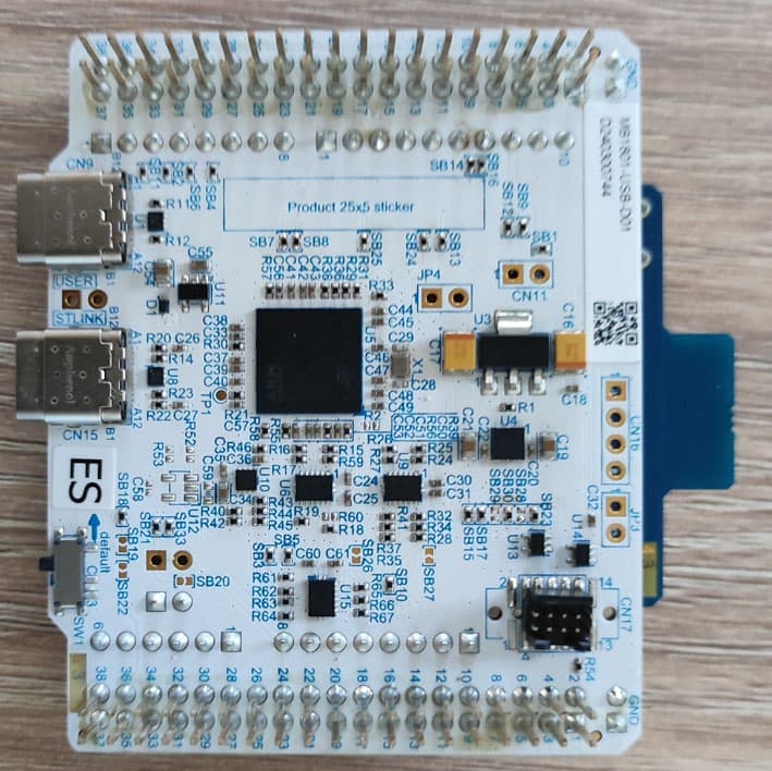
YCP-MB229300
Jun 08, 2026BLE RF evaluation board
Equipment Class
DTS - Digital Transmission System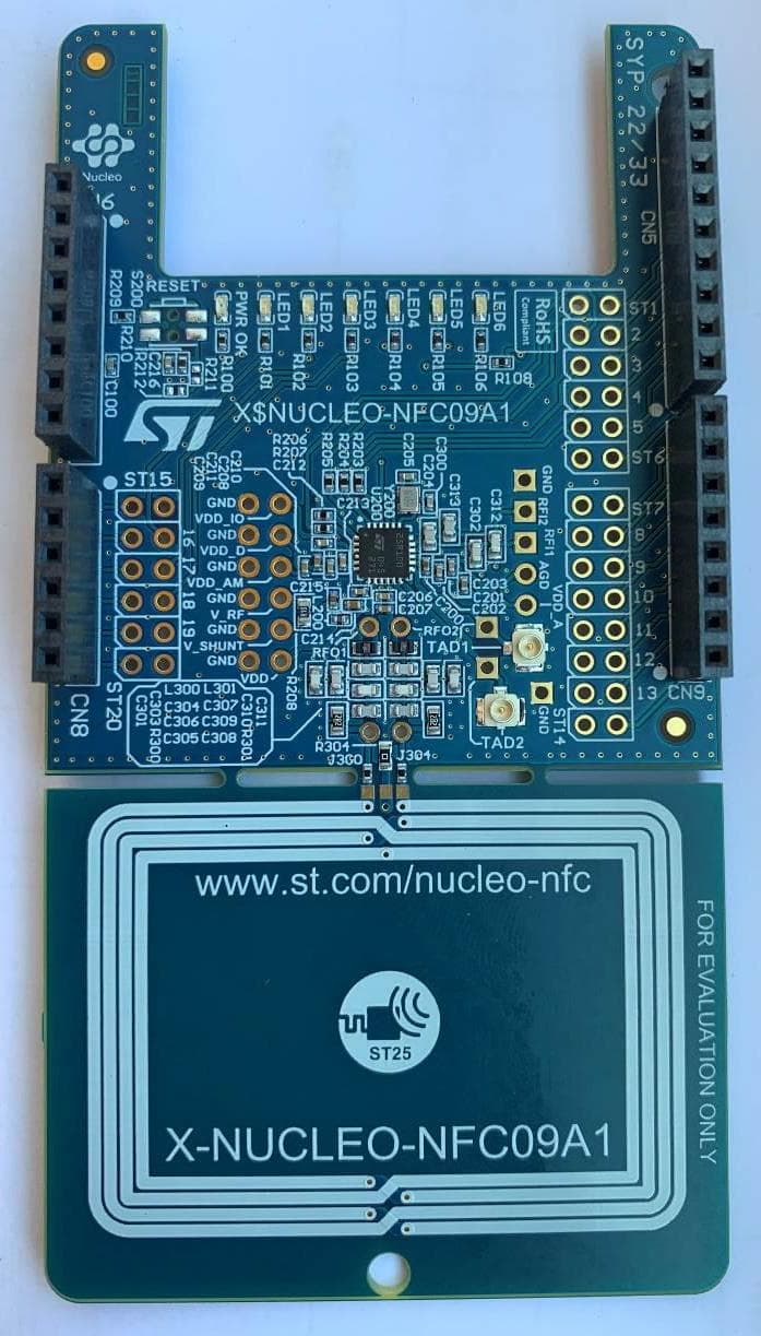
YCPNFC09A1
Oct 01, 2024NFC card reader evaluation board
Equipment Class
DXX - Part 15 Low Power Communication Device Transmitter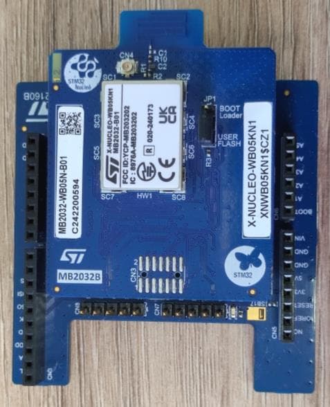
YCP-MB203202
Sep 10, 2024X-NUCLEO-WB05KN1
Equipment Class
DTS - Digital Transmission System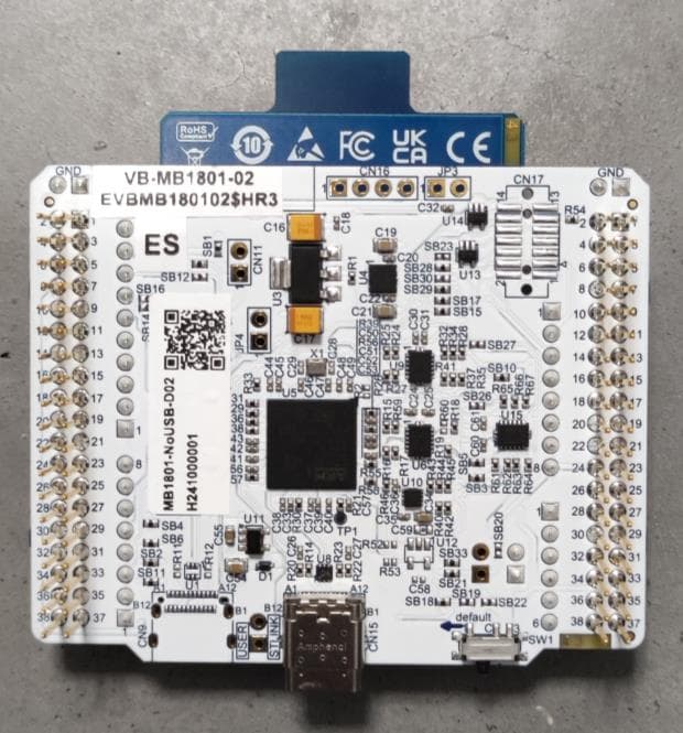
YCP-MB203200
Sep 05, 2024NUCLEO-WB05KZ
Equipment Class
DTS - Digital Transmission System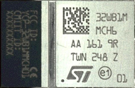
YCP-32WB1MMCH01
Jul 17, 2024Bluetooth Low Energy module
Equipment Class
DTS - Digital Transmission System