DZLCX3A18Cordless Transceiver Unit for X-Box
Logitech Inc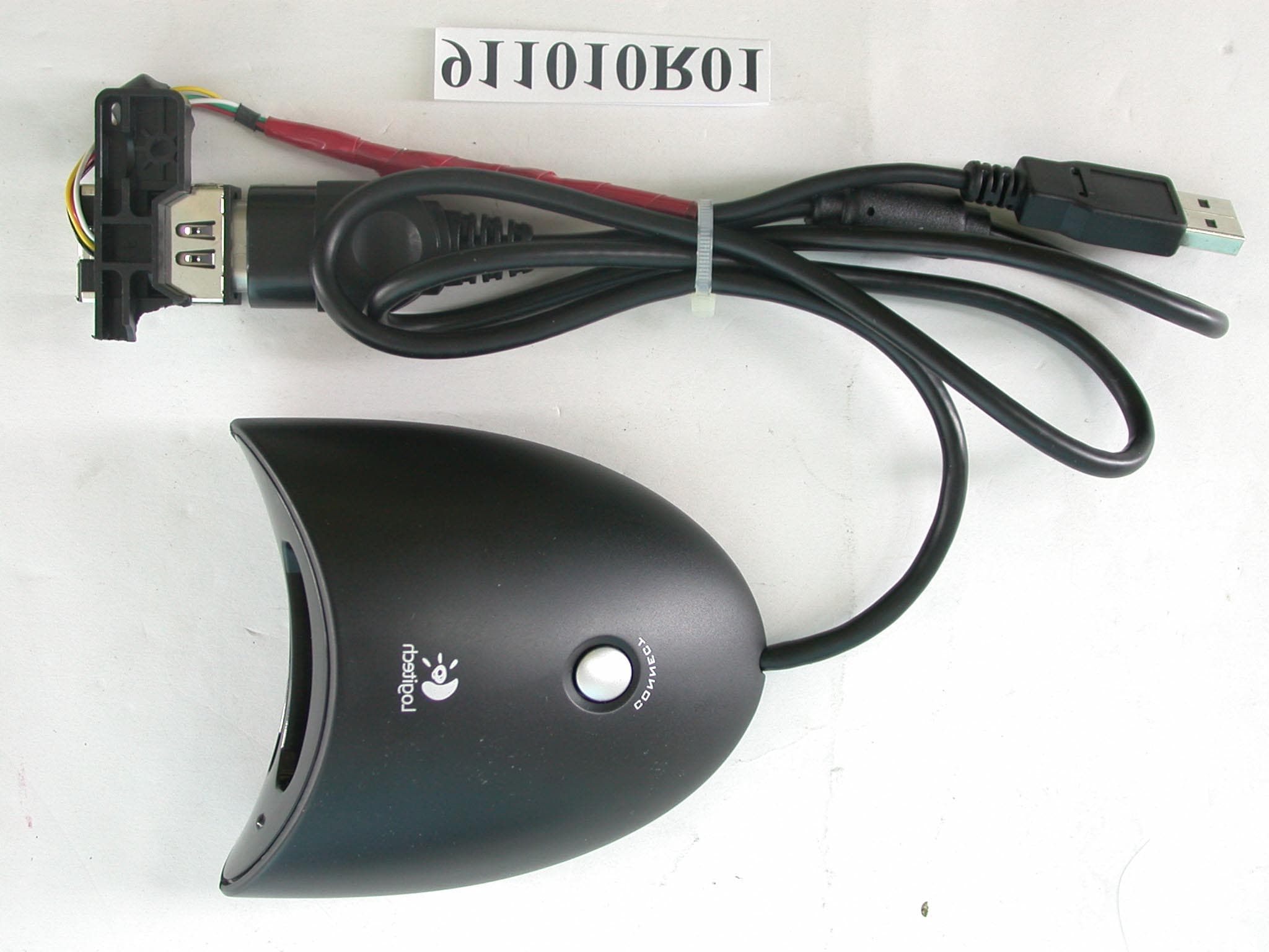
Click to zoom
Application Details
- Equipment Class
- DXX - Part 15 Low Power Communication Device Transmitter
- Date of Grant
- Nov 17, 2002
- Application Purpose
- Original Equipment
- Date of Application
- Nov 17, 2002
- Equipment Note
- Cordless Transceiver Unit for X-Box
- Frequency Range
- 2402.00000000 - 2480.00000000
- Company
- Logitech Inc
- Country
- United States
Documents & Files
Document Text
Text extracted from the exhibit documents filed with the FCC. Open a document above to read the original.
Users Manual
LOGITECH FAR EAST LTD. 6505 Kaiser Dive Fremont, CA 94555-3615 TEL: +1 510 713 4467 FAX: +1 510 713 5090 FEDERAL COMMUNICATIONS COMMISSION DECLARATION OF CONFORMITY (DoC) For the following equipment: Product Name: Logitech Cordless Controller for X-Box Model No.: G-RB7, C-X3A18 Trade Name: Logitech Is herewith confirmed to be in compliance with the requirements of ANSI C63.4 & FCC part 15 regulations. The test result has been shown in the ADT test report with number RF911010R01. And this compliance is subject to the following two conditions: This device may not cause harmful interference and, This device must accept any interference received, including interference that may cause undesired operation. The following local Manufacturer/Importer is responsible for this declaration: LOGITECH FAR EAST LTD. (Company Name) 6505 Kaiser Dive Fremont, CA 94555-3615 (Company Address) TEL +1 510 713 4777 FAX +1 510 713 5090 Bharat Shah/Compliance Engineer (Name) / (Title) (Signature) / (Date)
Cover Letter(s)
LOGITECH FAR EAST LTD. 6505 Kaiser Dive Fremont, CA 94555-3615 TEL: +1 510 713 4467 FAX: +1 510 713 5090 FCC ID: Federal Communications Commission Authorization and Evaluation Division Confidentiality Request Pursuant to Sections 0.457 and 0.459 of the Commission’s Rules, the Applicant hereby requests confidential treatment of information accompanying this Application as outlined below: Schematics Block Diagram The above materials contain trade secrets and proprietary information not customarily released to the public. The public disclosure of these matters might be harmful to the Applicant and provide unjustified benefits to its competitors. The Applicant understands that pursuant to Rule 0.457, disclosure of this Application and all accompanying documentation will not be made before the date of the Grant for this application. Sincerely, ----------------------------------------------- Bharat Shah/Compliance Engineer LOGITECH FAR EAST LTD. Tel: +1 510 713 4467 Fax:+1 510 713 5090 e-mail: [email protected]
Cover Letter(s)
POWER OF ATTORNEY To whom it may concern: We, the undersigned, LOGITECH FAR EAST LTD., hereby authorize Advance Data Technology Corporation (ADT) of Taiwan to act on our behalf in all matters relating to all processes required in the FCC Part 15C approval and any communication needed with the national authority. Any and all acts carried out by ADT on our behalf shall have the same effects as acts of our own. If you have any questions regarding the authorization, please don’t hesitate to contact us. Thank you! Sincerely yours, ------------------------------------------------------------------- Bharat Shah / Compliance Engineer LOGITECH FAR EAST LTD. Tel: +1 510 713 4467 Fax:+1 510 713 5090 e-mail: [email protected] LOGITECH FAR EAST LTD. 6505 Kaiser Dive Fremont, CA 94555-3615 TEL: +1 510 713 4467 FAX: +1 510 713 5090
Cover Letter(s)
American Telecommunications Certification Body Inc. 6731 Whittier Ave, McLean, VA 22101 November 14, 2002 RE: Logitech Inc. FCC ID: DZLCX3A18 After a review of the submitted information, I have a few comments on the above referenced Application. 1) The module schematic shows 2 antennas and the device only has 1. Additionally a 3rd antenna is shown on page 2 of the schematics. Please explain. 2) Since this device does not follow a typical Bluetooth protocol, please provide a plot showing the worse case transmit duration in 100 msec to validate the 24% duty cycle. 3) The schematics provided appear to be for the hand controller and not the transceiver unit. Please provide the proper schematics. 4) Since the device is intended for the X-Box and not as a PC peripheral, this device would not be subject to a DoC authorization but instead a Verification authorization for the digital device circuitry. Therefore please remove the DoC labeling information (FCC Logo, phrases "FOR HOME OR OFFICE USE" and "Tested to Comply with FCC Standards") from the label since it is not applicable to this device. 5) FYI, As long as the intended design of this device is for the X-Box and not as a PC peripheral, but gaming peripheral, the DoC statement is not necessary. Timothy R. Johnson Examining Engineer mailto: [email protected] The items indicated above must be submitted before processing can continue on the above referenced application. Failure to provide the requested information may result in application termination. Correspondence should be considered part of the permanent submission and may be viewed from the Internet after a Grant of Equipment Authorization is issued. Please do not respond to this correspondence using the email reply button. In order for your response to be processed expeditiously, you must submit your documents through the AmericanTCB.com website. Also, please note that partial responses increase processing time and should not be submitted. Any questions about the content of this correspondence should be directed to the sender.
Cover Letter(s)
Hello, Here is answer to your question: (1) The module has two PC Boards. (1) RF board and (2) Main board. Since, RF board is common across the board for the various Joy stick, it (RF Board) has two possible connections marking for Antenna. One is for connecting directly Antenna on the RF board. The other way is to have antenna connected to main board and connected to RF board using Co-axial wire. That is the reason RF board has two Antenna marking on it. Main Board has Antenna mounted to it, when there is no Antenna on the RF Board. Thus for this product, Antenna is connected to main Board and using coaxial cable it is connected to RF board. (2)Here is plot as requested. You may see total time is less than 2 msec for 100 msec span. (See attached file: TX_max_duty_cycle_for_adt.xls) (3) Will be provided soon (4) and (5) We will take FCC logo with "Home and Office use only" statement from unit which is connected to "XBOX" via hard wire. Thank you, Regards, Bharat Shah Tele : (510)-713-4777 Fax : (510)-713-4790 Subject: Re: Fwd: Review of Logitech Inc., FCC ID: DZLCX3A18 To: "Timothy R. Johnson" <[email protected]> Cc: [email protected], [email protected], [email protected] Page 1 of 1In 11/18/2002Printed for "Timothy R. Johnson" <[email protected]>
External Photos
Page 1 ANNEX PHOTOGRAPHS OF EUT Page 2 Page 3
Internal Photos
Page 4 Page 5 Page 6 Page 7 Page 8
Operational Description
FCC ID: DZLGRB7 FCC ID: DZLCX3A18 ADT No.911010R01 Operational Description The EUT (Logitech Cordless Controller for X-Box) includes two individual parts. One is the Gamepad which is held on the user’s hand, the other is Receiver Unit (a transceiver) which is connected with the host equipment. The Gamepad is powered by 6VDC battery and Receiver Unit is 5VDC from host equipment. This device is a Frequency Hopping device with 79 hopping frequencies. The declared output power is only +2.5mW. The hopping rate as well as the protocol is not the same as bluetooth, so it could not link with the bluetooth device.
RF Exposure Info
FCC ID: DZLGRB7 FCC ID: DZLCX3A18 ADT No.: 911010R01 Nov. 13, 2002 RF Exposure Compliance Statement The maximum RF output power measured is 4dBm or 2.51mW. The maximum Gain of the inverted-F antenna used is only -1dBi. The SAR limit would not be exceeded, even the entire maximum RF power output were absorbed by 1 gram of tissue, which is not possible with a typical RF circuit.
Schematics
AA BB CC DD EE 4 4 3 3 2 2 1 1 LNA in FOR FUTURE REVISIONS:============== ======== - optimize design of impedance match ing on LNA_IN & PA_OUT. - determine which of the 10nF caps on VCC_RF are needed. Ask TI:======- none. PA out Note: All inductors are spe cified 5% tol, but expected performance is 2% tol.. All capacitors are NPO type. Layout instru ctions: ============ ======= - keep traces to VCC caps very short. - LNA & PA grounding is critical. - VCC_LNA_A (J1) must be extremely short. - MU_1 & BB_CLK are very high speed signals (gnd return!).- Pour GND around CP_8MHz, PTT_R ES, MAIN_LF circuits. - RF traces are 50 Ohms +/ -10% microstrips. - keep all RF traces on top layer (no vias!). - layout PA_OUT lines symmetrically.- Follow layout order for C51, C52, C53. LOGITECH CON LOGITECH CON LOGITECH CON LOGITECH CONFI DENTIAL FIDENTIAL FIDENTIAL FIDENTIAL %%% WILL UPDATE COMPLETE IF FILTER, CHOOSE LOWER TOL. COMPONENTS %%% *L91="C91" COAX CABLE RF microstrip: 50 Ohm +/- 10% @ 2.440GHz. LFSN25N16C2450B R59 value is for 3.0V VCC_RF product version. 221625-0000 PA5.2 RF Module, Hagrid -- TR F6001 B 11 Tuesday, June 04, 2002 ES, PL 201625-0000 HAGRID TitleSize Document Number Rev Date: Sheet of Designed by PCB / part number Project Name TR_SWITCH_INVTR_SWITCH RSSI_ANA SLEEP_X IF_2IF_1 MIX_OUT1MIX_OUT2 SR_DATA DISC_OUT BB_CLK VREG_BB MIX_OUT1 IF_1IF_2 MIX_OUT2 SR_LESR_CLK MU_2MU_1 VCC_RF VCC_RF VCC_RF VCC_RFVCC_RF VCC_RF VCC_RF VCC_RF VCC_RF VCC_RF VCC_RF VCC_RF VCC_RF VCC_RF_SRC VCC_RF VCC_RF_SRC C60330pF 2% C18NM TP40 1 C7447pF TP10 1 C5510pF R960 Ohm L57NM C8610pF C54NM TP4 1 C52NM TP21 1 TP42 1 C6982pF 1% C19NM L992.7nH C9810pF C9510pF Y216MHz 30ppm C67NM C77 NM C79100pF R63 560K C92100pF C761nF TP7 1 L52NM TP17 1 C8410pF R530 Ohm TP22 1 C6675pF 1% TP11 1 C61NM TP19 1 R550 Ohm C836.8pF C17NM J51SIP_9 123456789 C622.2nF U4TRF6001 BGA_56GQE_10 A2 B2 C8B9 B3 A3H4 B4 H3 A4 A9 A5 J2 B5 J9 A6 C9 B6 A7 B7 D8 A8 J3 E9E8 J4 F9F8 H5 G9G8 J5 H9 J6 H6 J7 H7 J8 H8 A1B1 C1D1 E2E1 F1 G1 C2 G2 H1 F2 H2 J1 D2 B8D9 D3 D4 D5 D6 D7 E3 E4 E5 E6 E7 F3 F4 F5 F6 F7 G3 G4 G5 G6 G7 C4 C7 C5 C6 GND_VCO1 VCC_VCO1 MULTI_1MULTI_2 GND_VCO2 GND_MAIN_CPGND_LNA_PA1 VCC_VCO2 VCC_LNAB_PA2 MAIN_LF QUAD_OUT VCC_PLL_XTAL GND_SUB3 GND_XTAL IF1 XTAL_1 GND_MULTI XTAL_2 GND_PLL DS2 BB_CLK DS1 GND_LNAB_PA CAP1 GND_IF2 LNA_IN SLEEP_X SR_DATA GND_LNA_PA2 SR_Enable SR_CLK PA_OUT1 IF2 PA_OUT2 GND_LNA_PA3 VCC_IF1 VCC_PA1 VCC_IF2 GND_IF1_SUB GND_SUB1TR_SW_INVRSSI_ANAGND_SUB2VCC_LOGICGND_LOGICVREG_BBGND_MIXTR_SWCP_8MHzMIX_OUT1VCC_MIXMIX_OUT2VCC_LNA_APTT_RES VCC_MULTI CAP2 GND_1 GND_2 GND_3 GND_4 GND_5 GND_6 GND_7 GND_8 GND_9 GND_10 GND_12 GND_13 GND_14 GND_15 GND_16 GND_17 GND_18 GND_19 GND_20 GND_21 GND_27 GND_28 GND_29 GND_30 TP41 1 C50NM TP8 1 L59 5.6nH TP16 1 C7247pF C90NM R59 0 Ohm C15NM C81680pF C12NM R650 Ohm C59240pF 2% TP47 1 L545.6uH 2% R930 Ohm C7010pF ANT3ANT_PIFA_PAx 1 2 R57680 C11 NM C89 10pF TP14 1 C7310pF TP48 1 C82 6.8nF TP6 1 FLT1NM 1 4 3 2 GND IN GND OUT C7810pF C6327nF C711nF L91NM ANT2ANT_PIFA_PA2 1 2 C5675pF 1% C91NM C80 15nF TP44 1 R500 Ohm C9610pF TP2 1 C64 10nF 10% X7R C16NM TP13 1 L98 22nH C9410pF C210.5pF C13NM C14 10nF C8510pF L534.7uH 2% TP43 1 TP5 1 R560 Ohm C7510pF TP12 1 C65 27pF 2% NPO C20NM R700 Ohm L5110uH 2% R720 Ohm TP1 1 C57NM C5882pF 1% TP3 1 C87100pF L55NM L5610uH 2% C53NM TP20 1 R671.5K C51NM TP45 1 C68 27pF 2% NPO TP9 1 TP15 1 L60 1.2nH R520 Ohm C8810pF TP46 1 R6412K
Test Report
Possum project [ES021119] The hopping sequence is designed to hit each of 79 channels once every 316 ms producing a 4 ms frequency dwell period. The Master device's hopping cycle duration is identical in search and connected states. This 4 ms dwell period is decomposed as follows: - Master transmits during first 2 ms window for maximum 490 usec duration. - Slave transmits during second 2 ms window for maximum 490 usec duration. Master Search Mode Master connected Master/Slave Connection
Test Setup Photos
FCC ID: DZLGRB7 FCC ID: DZLCX3A18 Report No.: RF911010R01 37 Issued: Nov. 13, 2002 5 PHOTOGRAPHS OF THE TEST CONFIGURATION CONDUCTED EMISSION TEST FCC ID: DZLGRB7 FCC ID: DZLCX3A18 Report No.: RF911010R01 38 Issued: Nov. 13, 2002 RADIATED EMISSION TEST
Contact Information
Applicant
Paul Zahra(Regulatory Compliance Manager)
Technical Contact
Advance Data Technology CorporationVivi Wang
[email protected]+886-3-327-0910
13-1, Lane 19, WenShan 3rd., St. · Taoyuan · Taiwan
Non-Technical Contact
Advance Data Technology CorporationVivi Wang
[email protected]+886-3-327-0910
Test Firm
Bureau Veritas CPS (H.K.) Ltd. Taoyuan BranchTommy Wu
Technical Specifications
| # | Rule Parts | Frequency Range | Power Output |
|---|---|---|---|
| 1 | 15C | 2.40 GHz - 2.48 GHz | - |
Other Applications from Logitech Inc
DZLS00118
Oct 06, 2011AIR SPEAKER
Equipment Class
DTS - Digital Transmission System
DZLA00032
Aug 07, 2011Nano Receiver
Equipment Class
DSS - Part 15 Spread Spectrum Transmitter
DZLA00031
Jul 24, 2011Wireless Headset H600
Equipment Class
DSS - Part 15 Spread Spectrum Transmitter
DZLS00114
Jul 20, 2011Wireless module
Equipment Class
DSS - Part 15 Spread Spectrum Transmitter
DZLA00033
Jul 18, 2011Wireless Headset H800
Equipment Class
DSS - Part 15 Spread Spectrum Transmitter