F5306GS30552Cellular Alarm Communicator
Tyco Safety Products Canada Ltd.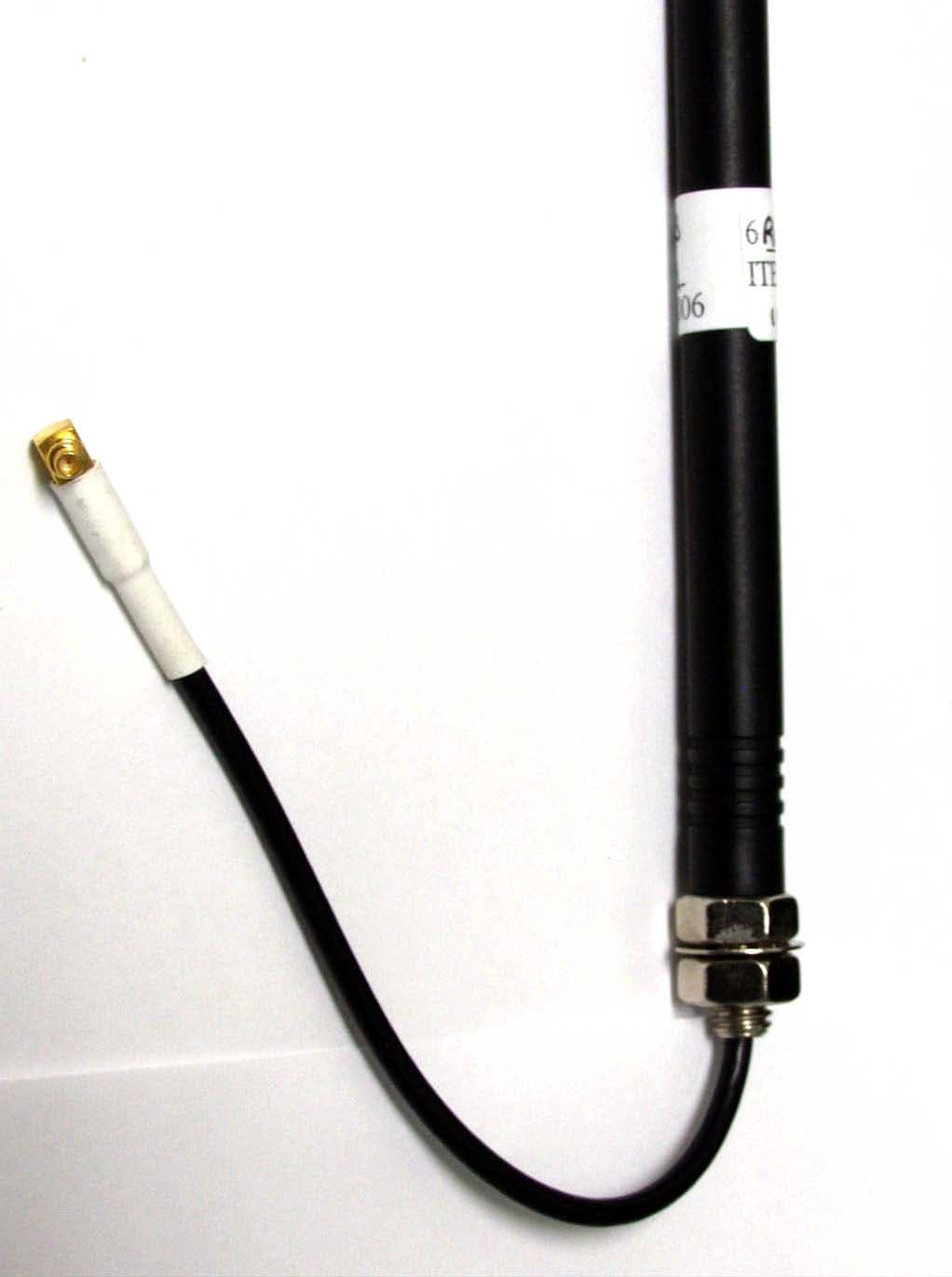
Click to zoom
Application Details
- Equipment Class
- PCB - PCS Licensed Transmitter
- Date of Grant
- Oct 29, 2006
- Application Purpose
- Original Equipment
- Date of Application
- Oct 29, 2006
- Equipment Note
- Cellular Alarm Communicator
- Frequency Range
- 1850.20000000 - 1909.80000000
- Country
- Canada
Documents & Files
Document Text
Text extracted from the exhibit documents filed with the FCC. Open a document above to read the original.
Users Manual
GSM-GPRS INTERFACE 2 GS3055-I INTRODUCTION....................................................................................................................3 FEATURES ............................................................................................................................3 Technical Specifications....................................................................................................... 3 Description............................................................................................................................ 4 IDENTIFICATION OF PARTS............................................................................................... 4 INSTALLING THE DEVICE ................................................................................................... 4 CONNECTING THE DEVICE................................................................................................ 4 STATUS LEDS....................................................................................................................... 5 OPERATING PRINCIPLES...................................................................................................5 Simulated Land Line .............................................................................................................5 SMS Function........................................................................................................................ 6 ContactID Mode.................................................................................................................... 6 Function Priority..................................................................................................................... 6 Simulated Land Line Priority ....................................................................................... 6 SMS or Contact ID Priority ........................................................................................... 6 ContactID Event Priority .............................................................................................. 6 ACTIVATING THE OUTPUTS ................................................................................................ 7 Activating/Deactivating Automatic Outputs......................................................................... 7 Activating/Deactivating Remote-control Outputs................................................................ 7 Bistable Outputs (for appliance management) ........................................................ 7 Monostable Outputs (for appliance management) .................................................. 7 PROGRAMMING THE SIM CARD VIA PC ........................................................................... 8 Viewing the Device Settings ...................................................................................... 8 Downloading the Device Settings ............................................................................. 8 Preliminary operations ................................................................................................ 8 Telephone Page.................................................................................................................... 8 Telephone Numbers.................................................................................................... 8 Prefix ............................................................................................................................ 9 Digit to Remove........................................................................................................... 9 SMS Dialler Page ................................................................................................................... 9 Main window............................................................................................................... 9 Priority.......................................................................................................................10 Pay-as-you-go balance message........................................................................... 1 0 Periodic message .................................................................................................... 1 0 Outputs Page...................................................................................................................... 1 0 Output Settings........................................................................................................ 1 0 Access Code........................................................................................................... 1 0 Contact ID Page .................................................................................................................. 1 0 Telephone numbers to call ....................................................................................... 1 1 Events description..................................................................................................... 1 1 Send over GPRS ........................................................................................................ 1 1 Periodic Reports ........................................................................................................ 1 1 GPRS page .......................................................................................................................... 1 1 Access Point Name ................................................................................................... 1 1 Receiver IP address and Port ................................................................................... 1 1 APNs User Name and Password ............................................................................... 1 1 Telephone numbers to decode................................................................................ 1 1 SIM number ............................................................................................................... 1 1 DNIS................................…
Text truncated - open the document above for the full version.
Cover Letter(s)
October 4, 2006 Nemko Canada Inc 303 River Road Ottawa, Ontario, Canada K1V 1H2 Attn: Director of Certification Authority to Act as Agent On our behalf, I appoint Nemko Canada Inc., 303 River Road, Ottawa, Ontario, Canada K1V 1H2 to act as our agent in the preparation of this application for equipment certification. I certify that submitted documents properly describe the device or system for which equipment certification is sought. I also certify that each unit manufactured, imported or marketed, as defined in the Federal Communications Commission’s regulations will have affixed to it a label identical to that submitted for approval with this application. For instances where our authorized agent signs the application for certification on our behalf, I acknowledge that all responsibility for complying with the terms and conditions for certification, as specified by Nemko Canada Inc, still resides with Digital Security Controls, 3301 Langstaff Road, Concord, Ontario Canada L4K 4L2. Dated this 4 th Day ofOctober 20 06 Agency agreement expiration date: October 4, 2006 By: Dan Nita Signature Printed Title: Approvals Manager On behalf of : Digital Security Controls Telephone: 905-760-3000, Ext. 2706
Cover Letter(s)
October 4, 2006 Equipment Authorisation Division Federal Communications Commission 7435 Oakland Mills Road Columbia, MD 21046 FCC ID: F5306GS30552 Product Name: DSC GS3055-I Model: GS3055-2 Request for Confidentiality Pursuant to Sections 0.457 and 0.459 of the commissions rules, we hereby request that the following documents be held confidential: • Schematics • Block diagram • Operational description These materials contain trade secrets and proprietary information and are not customarily released to the public. The public disclosure of this information might be harmful to the company and provide unjustified benefits to our competitors. Dated this 4 th Day ofOctober 20 06 By: Dan Nita Signature Printed Title: Approval Manager On behalf of : Digital Security Controls Telephone: 905-760-3000, Ext. 2706
Cover Letter(s)
Bentel FCC IC report use GS3055-2 v2.doc September 29, 2006 Motorola authorizes DSC Toronto with their certified test lab (NEMKO CANADA INC) to use the g24 documentation supplied by Motorola for testing and certification of DSC Toronto GS3055-2 for FCC and IC requirements. Documents supplied for use includes, test reports and the actual Motorola exhibits used for the g24 FCC submission, which were supplied under NDA. The following exhibits may be used for the filing with the FCC, but you must protect the confidentiality of the info in your filing process. DSC Toronto. and their test lab must request confidentiality with FCC when submitting the three exhibits below. Exhibit 4 Block diagram Exhibit 5 Schematics Exhibit 12 Operational Description. NEMKO CANADA INC representing DSC Toronto. in submitting for FCC and IC approval of the GS3055-2 and may use supporting documents supplied by Motorola on the Motorola g24 data module including test reports, and exhibits and is authorized to use the company name “Motorola”, product name “g24” and software version number “0C.04.76R” solely for the certification process of DSC Toronto GS3055-2 product which has the Motorola g24 data module embedded. Sincerely, Steve Gump Engineering Manager OEM Embedded Modules Motorola Inc.
ID Label/Location Info
18008055 Rev 001 GS3055-2 MULTI-LISTING LABEL.eps Source file: [18008055R001_GS3055-2_MULTI-LISTING_UL-ULC-FCC-WEEE_LB.eps] October 4, 2006 35 mm Digital Security Controls ISO9001 Registered 3301 Langstaff Road, Concord Ontario, Canada L4K 4L2 Phone: 905-760-3000 Toll Free: 1-888-888-7838 Fax: 905-760-3020 Dashed line indicates cut edge of label (will not print) Label to be printed on white UL approved self-adhesive Mylar type material with indelible black ink Label shown actual size NOTE: All UL and ULC Labels shall be printed by a UL Listed printing facility. The issue number (when applicable) shall be requested from ULC Label Ordering Department (Phone: 416-757-5250) the printing facility at the time of printing. 60mm 18008055 Rev 001 Digital Security Controls, Toronto, Canada MADE IN CANADA FABRIQUE AU CANADA Model: GS3055-2 FCC ID: F5306GS30552 IC:160A-GS30552 This device complies with Part 15 Class B of the FCC rules. Operation is subject to the following two conditions: (1) This device May not cause harmful interference and (2) this device must accept any interference received, including interference that may cause undesired operation. For use in dry indoor locations only. For installation refer to NFPA70, 72 and Installation Manual 2900xxxx. SUBSCRIBER’S UNIT - ACCESSORY FIRE ALARM AND/OR BURGLARY HOUSEHOLD FIRE AND BURGLARY WARNING SYSTEM CONTROL UNIT ASSEMBLY ALSO SUITABLE FOR USE AS A COMMERCIAL BURGLAR ALARM SYSTEM ACCESSORY This Class B digital apparatus complies with Canadian ICES-003. Cet appareil numérique de la classe B est conforme à la norme NMB-003 du Canada. ISSUE NO. 1 8 0 0 8 0 5 4 R e v 0 0 1 D ig ital Sec u r ity C on trol s, T o ronto, C a n ad a M A D E IN C A N A D A F A B R I Q U E A U C A N A D A M o d e l: G S 3 0 5 5 - I F C C I D : F 5 3 0 6 G S 3 0 5 5 IC : 1 6 0 A - 0 6 G S 3 0 5 5 This device complies with Par t 15 Class B of the FCC rules. Operation is su bject to the following two conditions: (1) This devic e May not cause harmful inter ference and (2) this d evice must accept any int erference received, including inter ference that may cause undesired operation. For use in dry indoor locations only. For installation refer to NFP A70, 72 and Installation Manu al 2900xxxx . S U B S C R IB E R ’S U N IT - A C C E S S O R Y F IR E A L A R M A N D / O R B U R G L A R Y H O U S E H O L D F IRE A N D B U R G L A R Y W A R N IN G S YS T E M C O N T R O L U N IT A S S E M B LY A L S O S U IT A B L E F O R U S E A S A C O M M E R C IA L B U R G LA R A LA R M S Y S T E M A C C E S S O R Y T h is C la s s B d ig i ta l ap p a ra tu s c o m p lie s w it h C a n a d ia n IC E S - 0 0 3. C e t a p p a re il n u m é riq u e d e la c la s s e B e s t c o n fo rm e à la n o rm e N M B - 0 0 3 d u C a n a d a . ISSUE NO. Top of metal cabinet showing label location (not actual size)
Internal Photos
APPLICANT: MOTOROLA INC. FCC ID: IHDT56FV1 Front View (With Shield) Rear View (With Shield) 2 EXHIBIT 9 APPLICANT: MOTOROLA INC. FCC ID: IHDT56FV1 Front View (Shields Removed) Rear View (Shields Removed) 1 EXHIBIT 9
Parts List/Tune Up Info
Pagina 1 di 2 BENTEL SECURITY s.r.l. - Lista dei materiali Nome prodotto : B052 SCHEDA INTERFACCIA GSM/GPRS x N.A. Processi di lavorazione : SR+PA+PM+PW Revisione schema : A Data : 18-09-06PCB : B052_P1 Qta Referenza Valore Codice Descrizione Mnt 1 FM2 B052 PCBB052_P1 Circuito stampato B052_P1 1 ACC1 PS-Libr ACEPSIM06COPCER PORTA SIM SMD 6VIE COPERCHIO E CERNIERA SR 5 C14 C15 C31 C32 C37 470p CAPCCN0J0470805 CONDENSATORE SMD NP0 5% 470pF 0805 SR 9 C11 C17 C23 C26 C38 C40 C48 C54 C56 1n CAPCCXRM1100805 CONDENSATORE SMD X7R 10% 1nF 0805 SR 1 C36 2n2 CAPCCXRM1220805 CONDENSATORE SMD X7R 10% 2,2nF 0805 SR 3 C5 C41 C58 4n7 CAPCCXRM1470805 CONDENSATORE SMD X7R 10% 4,7nF 0805 SR 4 C1 C13 C43 C53 10n CAPCCXRM2100805 CONDENSATORE SMD X7R 10% 10nF 0805 SR 22 C7 C9 C10 C20 C21 C22 C33 C44 C46 C47 C49 C50 C51 C55 C59 C62 C63 C66 C68 C70 C71 C72 47n CAPCCXRM2470805 CONDENSATORE SMD X7R 10% 47nF 50V 0805 SR 5 C16 C19 C27 C45 C57 100n CAPCCXRM3100805 CONDENSATORE SMD X7R 10% 100nF 50V 0805 SR 1 C6 220n CAPCCXRM3220805 CONDENSATORE SMD X7R 10% 220nF 0805 SR 1 C25 1U CAPCCXRM4100805 CONDENSATORE SMD X7R 10% 1uF 25V 0805 SR 1 J1 Molex52991 CONNRFV7005052991 CONNETTORE SMD FEM.VA.70V. P.0,5 M.52991 SR 1 D13 DB107S DDOSPONDB107S DIODO SMD RADDR.A PONTE 1A 1000V DB107S SR 7 D4 D7 D12 D16 D19 D22 D24 4148 DDOSSIG1N4148 DIODO SMD SEGNALE MINIMELF LL4148 SR 2 D21 D23 BAV70 DDOSSIGBAV70 DIODO SMD SEGNALE 'Doppio diodo' BAV70 SR 3 D5 D6 D8 BAV99 DDOSSIGBAV99 Diodo SMD Segnale 'doppio diodo' BAV99 SR 1 D2 BAS85 DDOSSTKBAS85 DIODO SMD SCHOTTKY 200mA 30V SOD80 BAS85 SR 1 D1 SS14 DDOSSTKSS14 DIODO SMD SCHOTTKY 1A 40V DO-214AC SS14 SR 2 D10 D18 7V5 DDOSZEN7V5MW500 DIODO SMD ZENER 7,5 Volt 500mW SR 1 U10 L78L33 INTCLINL78L33ACD INTEGRATO SMD REGOL.TENS.3,3V L78L33ACD SR 1 U3 LM317 INTCLINLM317 INTEGRATO SMD REG.TENSIONE D2PAK-3 LM317 SR 1 U1 LM324 INTCLINLM324 INTEGRATO SMD 4 AMPLIF. OPERAZ. LM324 SR 1 U2 LM339 INTCLINLM339 INTEGRATO SMD 4 COMPARATORI LM339 SR 1 U8 LM358 INTCLINLM358 INTEGRATO SMD 2 AMPL.OP LM358 SR 1 U11 TPS76301 INTCLINTPS76301 INTEGRATO SMD REGOL.TENS.SOT-23 TPS76301 SR 1 U6 LPC2103 INTCMPRLPC2103 INTEGRATO SMD MICRO FLASH LQFP48 LPC2103 SR 2 U5 U7 CNY17 OPTATRNSDCNY17-2 FOTOACCOPPIATORE SMD TRANSISTOR CNY17-2 SR 1 R111 536 RESSMDF05361805 RESISTENZA CHIP 1% 536 OHM 1/10 W 0805 SR 1 R72 1k RESSMDF11001805 RESISTENZA CHIP 1% 1 KOHM 1/10 W 0805 SR 1 R1 4k7 RESSMDF14701805 RESISTENZA CHIP 1% 4,7 KOHM 1/10 W 0805 SR 1 R23 18k7 RESSMDF21871805 RESISTENZA CHIP 1% 18,7 KOHM 1/10 W 0805 SR 1 R85 100k RESSMDF31001805 RESISTENZA CHIP 1% 100 KOHM 1/10 W 0805 SR 1 R126 220k RESSMDF32201805 RESISTENZA CHIP 1% 220 KOHM 1/10 W 0805 SR 1 R155 0 RESSMDJ-0001805 Resistenza CHIP 5% 0 OHM 1/10 W 0805 SR 1 R13 22 RESSMDJ00221805 RESISTENZA CHIP 5% 22 OHM 1/10 W 0805 SR 1 R94 47 RESSMDJ00471805 RESISTENZA CHIP 5% 47 OHM 1/10 W 0805 SR 2 R24 R64 330 RESSMDJ03301805 RESISTENZA CHIP 5% 330 OHM 1/10 W 0805 SR 2 R30 R49 470 RESSMDJ04701805 RESISTENZA CHIP 5% 470 OHM 1/10 W 0805 SR 5 R15 R18 R21 R25 R31 680 RESSMDJ06801805 RESISTENZA CHIP 5% 680 OHM 1/10 W 0805 SR 4 R47 R62 R99 R110 1k RESSMDJ11001805 RESISTENZA CHIP 5% 1 KOHM 1/10 W 0805 SR 2 R88 R107 1k5 RESSMDJ11501805 RESISTENZA CHIP 5% 1,5 KOHM 1/10 W 0805 SR 1 R98 2k RESSMDJ12001805 RESISTENZA CHIP 5% 2 KOHM 1/10 W 0805 SR 5 R39 R50 R54 R102 R104 2k2 RESSMDJ12201805 RESISTENZA CHIP 5% 2,2 KOHM 1/10 W 0805 SR 11 R8 R16 R26 R65 R79 R81 R83 R108 R115 R116 R125 3k3 RESSMDJ13301805 RESISTENZA CHIP 5% 3,3 KOHM 1/10 W 0805 SR 5 R17 R42 R44 R60 R123 4k7 RESSMDJ14701805 RESISTENZA CHIP 5% 4,7 KOHM 1/10 W 0805 SR 1 R74 5k6 RESSMDJ15601805 RESISTENZA CHIP 5% 5,6 KOHM 1/10 W 0805 SR 2 R117 R118 6k8 RESSMDJ16801805 RESISTENZA CHIP 5% 6,8 KOHM 1/10 W 0805 SR 27 R2 R4 R10 R36 R40 R43 R45 R55 R61 R70 R75 R76 R89 R91 R95 R97 R101 R106 R109 R119 R124 R127 R128 R129 R130 R153 R154 10k RESSMDJ21001805 RESISTENZA CHIP 5% 10 KOHM 1/10 W 0805 SR 3 R7 R11 R14 15k RESSMDJ21501805 RESISTENZA CHIP 5% 15 KOHM 1/10 W 0805 SR 3 R29 R51 R103 22k RESSMDJ22201805 RESISTENZA CHIP 5% 22 KOHM 1/10 W 0805 SR 12 R22 R27 R35 R37 R38 R48 R78 R86 R105 R120 R121 R152 47k RESSMDJ24701805 RESISTENZA CHIP 5% 47 KOHM 1/10 W 0805 SR 7 R20 R28 R52 R67 R87 R112 R157 100k RESSMDJ31001805 RESISTENZA CHIP 5% 100 KOHM 1/10 W 0805 SR 1 R3 120k RESSMDJ31201805 RESISTENZA CHIP 5% 120 KOHM 1/10 W 0805 SR 3 R6 R93 R133 220k RESSMDJ32201805 RESISTENZA CHIP 5% 220 KOHM 1/10 W 0805 SR 2 R113 R114 330k RESSMDJ33301805 RESISTENZA CHIP 5% 330 KOHM 1/10 W 0805 SR 1 R59 470k RESSMDJ34701805 RESISTENZA CHIP 5% 470 KOHM 1/10 W 0805 SR 1 R140 1M RESSMDJ41001805 RESISTENZA CHIP 5% 1 MOHM 1/10 W 0805 SR 1 R100 2M2 RESSMDJ42201805 RESISTENZA CHIP 5% 2,2 MOHM 1/10 W 0805 SR 1 Q14 FQD17P06 TRNSMOPFQD17P06 TRANSISTOR SMD MOSFET C.P 60V FQD17P06 SR 1 Q16 HUF76407 TRNSMOPHUF76407D TRANSISTOR SMD P.MOSF.C.N HUF76407D3S SR 1 Q3 MJD32 TRNSPOTMJD32C TRANSISTOR SMD POTENZ.PNP 3A DPAK MJD32C SR 6 Q1 Q2 Q6 Q8 Q9 Q28 BC817 TRNSSIGBC817 TRANSISTOR SMD SEGNALE A5 45V NPN BC817B SR 6 Q10 Q12 Q17 Q26 Q27 Q33 BC847 TRNSSIGBC847 TRANSISTOR SMD SEGNALE A1 45V NPN BC847B SR 1 Q15 BC857 TRNSSIGBC857 TRANSISTOR SMD SEGNALE A1 45V PNP BC857B SR Pagina 2 di 2 BENTEL SECURITY s.r.l. - Lista dei materiali Nome prodotto : B052 SCHEDA INTERFACCIA GSM/GPRS x N.A. Processi di lavorazione : SR+PA+PM+PW Revisione schema : A Data : 18-09-06PCB : B052_P1 Qta Referenza Valore Codice Descrizione Mnt 2 D14 D15 SBYV27 DDOTSWTSBYV27-150 Diodo Switch 2A 100V SBYV27-150 PA 2 D11 D17 4007 DDOTRET1N4007 DIODO RETTIFICATORE 1N4007 PA 1 R63 4M7 RESSTRJ4470M250 RESISTENZA STRATO 5% 4,7 MOHM 1/4 W PA 1 R73 1M RESSTRJ4100M250 RESISTENZA STRATO 5% 1 MOHM 1/4 W PA 5 R34 R53 R56 R58 R69 47k RESSTRJ2470M250 RESISTENZA STRATO 5% 47 KOHM 1/4 W PA 2 R68 R151 22k RESSTRJ2220M250 RESISTENZA STRATO 5% 22 KOHM 1/4 W PA 1 R9 15k RESSTRJ2150M250 RESISTENZA STRATO 5% 15 KOHM 1/4 W PA 4 R41 R57 R77 R96 10k RESSTRJ2100M250 RESISTENZA STRATO 5% 10 KOHM 1/4 W PA 1 R71 1k RESSTRJ1100M250 RESISTENZA STRATO 5%…
Text truncated - open the document above for the full version.
Parts List/Tune Up Info
GS3055-I DSC Cellular Alarm Communicator 850 – 1900 MHz GSM dual band antenna Manufacturer Bondale Industries Ltd. Model Number: G-RA-10102(323-030/F) The GSM frequencies for these bands are: Low band: TX: 824-849 MHz; RX: 869-893MHz. Low tuning frequency: 858MHz (±20MHz) High band: TX: 1850-1910MHz; RX : 1930-1990MHz. High tuning frequency: 1920MHz (±30MHz) Expected Return Loss on the tuning frequencies: Less than - 10dB Refer below to the electrical specifications and mechanical specifications. Radiator dimension specification: Inner radial length: 63mm Outer spring: 9+ ½ turns (with a short circuit on first turn). 850 – 1900MHz GSM ANTENNA • Electrical specifications Tuning frequencies: 858MHz (±20MHz) and 1920 MHz (±30MHz) Expected Return Loss on the tuning frequencies: Less than -10dB • Return Loss diagram of antenna sample Fig 1. Low band: Tuning frequency: 867MHz, Return Loss: -33,83dB Fig 2. High band: Tuning frequency: 1901MHz, Return Loss: -16,28dB • Picture of the sample:
Parts List/Tune Up Info
October 10, 2006 Product Name: DSC Cellular Alarm Communicator GS3055-I Model: GS3055-2 FCC ID: F5306GS30552 IC: 160A-GS30552 To Whom It May Concern: This is to confirm that for the DSC GS3055-I Cellular Alarm Communicator, Model GS3055-2 there is no end user/service person tune up procedure and the final tune up is all done at the factory. Respectfully yours, Dan Nita Approvals Manager 1
RF Exposure Info
1 1 August 31, 2005 SAR Test Report for Motorola Mobile Cellular Phone FCC ID IHDT56FV1. Prepared by: Steven Hauswirth, Principal Staff Engineer Motorola Personal Communications Sector Product Safety & Compliance Laboratory Libertyville, Illinois The Motorola Personal Communications Sector Product Safety & Compliance Laboratory has evaluated the mobile cellular phone, FCC ID IHDT56FV1, for the need to conduct SAR evaluation. Due to the design and installation of this product, it is not possible to conduct SAR evaluation. This is because Motorola neither manufactures or supplies the antenna(s) that will be used in the installation of this product. Therefore, this product will be evaluated as a mobile device per 47 CFR §1.1310 titled “Radiofrequency radiation exposure limits”, generally referred to as MPE limits. In 47 CFR § 2.1091, paragraph (b) defines a mobile device as “a transmitting device designed to be used in other than fixed locations and to generally be used in such a way that a separation distance of at least 20 centimeters is normally maintained between the transmitter’s radiating structure(s) and the body of the user or nearby persons.” This product is intended to be installed into a vehicle such that the unit is physically secured at one location. In the installation guide supplied with the product, Motorola has made the following statement: “IMPORTANT: To meet the FCC’s RF Exposure Guidelines, the antenna should be installed so there is at least 20 cm of separation between the body of the user and nearby persons and the antenna”. Based on the installation of the transceiver and the antenna, the transmitters radiating structure is more than 20 centimeters from the user. Thus, this product is a “mobile device” as defined in section § 2.1091 paragraph (b). Table 1 (B) of 47 CFR §1.1310 lists the limits for MPE for the General Population. Since the mobile cellular phone operates in the 800MHz cellular band and 1900MHz PCS band, the listed limit of f/1500 applies. The lowest transmit frequency for this product is 824.04 MHz, resulting in a MPE limit of 0.549 mW/cm 2 . Since Motorola neither manufactures or supplies the antenna(s) that will be used in the installation of this product, it is not possible to measure the MPE of the actual device as it is installed per the installation manual. Therefore a calculation of MPE will be described in the next paragraph. The MPE of a radiating structure can be calculated by knowing the transmit EIRP and the distance at which MPE is being calculated. In this case MPE will be calculated at 20 cm, which is the minimum separation between the body of the user and nearby persons and the antenna. The maximum sourced based time-averaged transmit power for this product is 0.50 Watts in the GPRS 850 mode and 0.25 Watts in the GPRS 1900 mode. At 824.04MHz, when installed using a combined cable loss and antenna gain of a maximum of 6.9 dBi the maximum ERP will be less than 1.5 Watts. The model used for calculating power density in OET Bulletin 65, Edition 97-01, is the spherical model. Using this spherical model, 0.48mW/cm2 is achieved at a distance of 20cm from the antenna at 824.04MHz. This is below the limit of 0.55 mW/cm2. For GSM 1900, the power density is 0.24mW/cm2, which is below the limit of 1.00 mW/cm2. Therefore, by requiring the user and nearby persons to remain at least 20cm from the antenna, the MPE is not exceeded.
RF Exposure Info
Prediction of MPE limit at a given distance Equation from page 18 of OET Bulletin 65, Edition 97-01where: S = power density P = power input to the antennaG = power gain of the antenna in the direction of interest relative to an isotropic radiatorR = distance to the center of radiation of the antenna Maximum peak output power at antenna input terminal: 27.00 (dBm) Maximum peak output power at antenna input terminal: 501.1872336 (mW) Antenna gain(typical): 1 (dBi) Maximum antenna gain: 1.258925412 (numeric) Prediction distance: 20 (cm) Prediction frequency: 824.04 (MHz) MPE limit for uncontrolled exposure at prediction frequency: 0.54936 (mW/cm^2) Power density at prediction frequency: 0.125525 (mW/cm^2) Maximum allowable antenna gain: 7.411268897 (dBi) Margin of Compliance: 6.411268897 2 4 R PG S π =
RF Exposure Info
Prediction of MPE limit at a given distance Equation from page 18 of OET Bulletin 65, Edition 97-01where: S = power density P = power input to the antennaG = power gain of the antenna in the direction of interest relative to an isotropic radiatorR = distance to the center of radiation of the antenna Maximum peak output power at antenna input terminal: 24.00 (dBm) Maximum peak output power at antenna input terminal: 251.1886432 (mW) Antenna gain(typical): -2.6 (dBi) Maximum antenna gain: 0.549540874 (numeric) Prediction distance: 20 (cm) Prediction frequency: 1850 (MHz) MPE limit for uncontrolled exposure at prediction frequency: 1 (mW/cm^2) Power density at prediction frequency: 0.027462 (mW/cm^2) Maximum allowable antenna gain: 13.01269855 (dBi) Margin of Compliance: 15.61269855 2 4 R PG S π =
Test Report
Hermon Laboratories Ltd. P.O.Box 23, Binyamina 30500, Israel Tel. +972 4628 8001 Fax. +972 4628 8277 E-mail: [email protected] Page 1 of 153 Report ID: MOTRAD_FCC.16719_rev1.doc Date of Issue: November 2005 Electrical TEST REPORT ACCORDING TO: FCC parts 22, 24 and part 15 subpart B FOR: Motorola Communications Israel Ltd. QuadBand GSM module 850/1900 MHz Model:G24 FCC ID:IHDT56FV1 This report is in conformity with ISO/ IEC 17025. The A2LA logo endorsement applies only to the test methods and the standards that are listed in the scope of Hermon Laboratories accreditation. The test results relate only to the items tested. This test report shall not be reproduced in any form except in full with the written approval of Hermon Laboratories Ltd. Report ID: MOTRAD_FCC.16719_rev1.doc Date of Issue: November 2005 Page 2 of 153 Table of contents 1 Applicant information..................................................................................................................................................... 3 2 Equipment under test attributes .................................................................................................................................... 3 3 Manufacturer information .............................................................................................................................................. 3 4 Test details.................................................................................................................................................................... 3 5 Tests summary.............................................................................................................................................................. 4 6 EUT description............................................................................................................................................................. 5 6.1 General information....................................................................................................................................................... 5 6.2 Support and test equipment .......................................................................................................................................... 5 6.3 Operating frequencies ................................................................................................................................................... 5 6.4 Changes made in the EUT ............................................................................................................................................ 5 6.5 Transmitter characteristics ............................................................................................................................................ 6 7 Transmitter tests according to 47CFR part 22 requirements......................................................................................... 7 7.1 Peak output power ........................................................................................................................................................ 7 7.2 Occupied bandwidth test ............................................................................................................................................. 10 7.3 Spurious emissions at RF antenna connector test ...................................................................................................... 17 7.4 Field strength of spurious emissions ........................................................................................................................... 42 7.5 Frequency stability test................................................................................................................................................ 60 8 Transmitter tests according to 47CFR part 24 requirements....................................................................................... 63 8.1 Peak output power ...................................................................................................................................................... 63 8.2 Occupied bandwidth test ............................................................................................................................................. 66 8.3 Spurious emissions at RF antenna connector test ...................................................................................................... 73 8.4 Field strength of spurious emissions ......................................................................................................................... 101 8.5 Frequency stability test.............................................................................................................................................. 122 9 Unintentional radiation tests according to 47CFR part 15 subpart B requirements ................................................... 125 9.1 Conducted emissions ................................................................................................................................................ 125 9.2 Radiated emissions .........................................................................................…
Text truncated - open the document above for the full version.
Contact Information
Applicant
Dan Nita(Approvals Manager)
Test Firm
Hermon Laboratories Ltd.Alexander Usoskin
Technical Specifications
| # | Rule Parts | Frequency Range | Power Output | Emission | Tolerance |
|---|---|---|---|---|---|
| 2 | 24E | 1.85 GHz - 1.91 GHz | 1.04 W | 277KGXW | 2.5 ppm |
Other Applications from Tyco Safety Products Canada Ltd.
F53252RFLOCK
Jun 05, 2026IQ Lock-PGP, IQ Lock Touch-PGP
Equipment Class
DTS - Digital Transmission System
F5325PGPDC9
Apr 27, 2026PowerG wireless transceiver module
Equipment Class
DSS - Part 15 Spread Spectrum Transmitter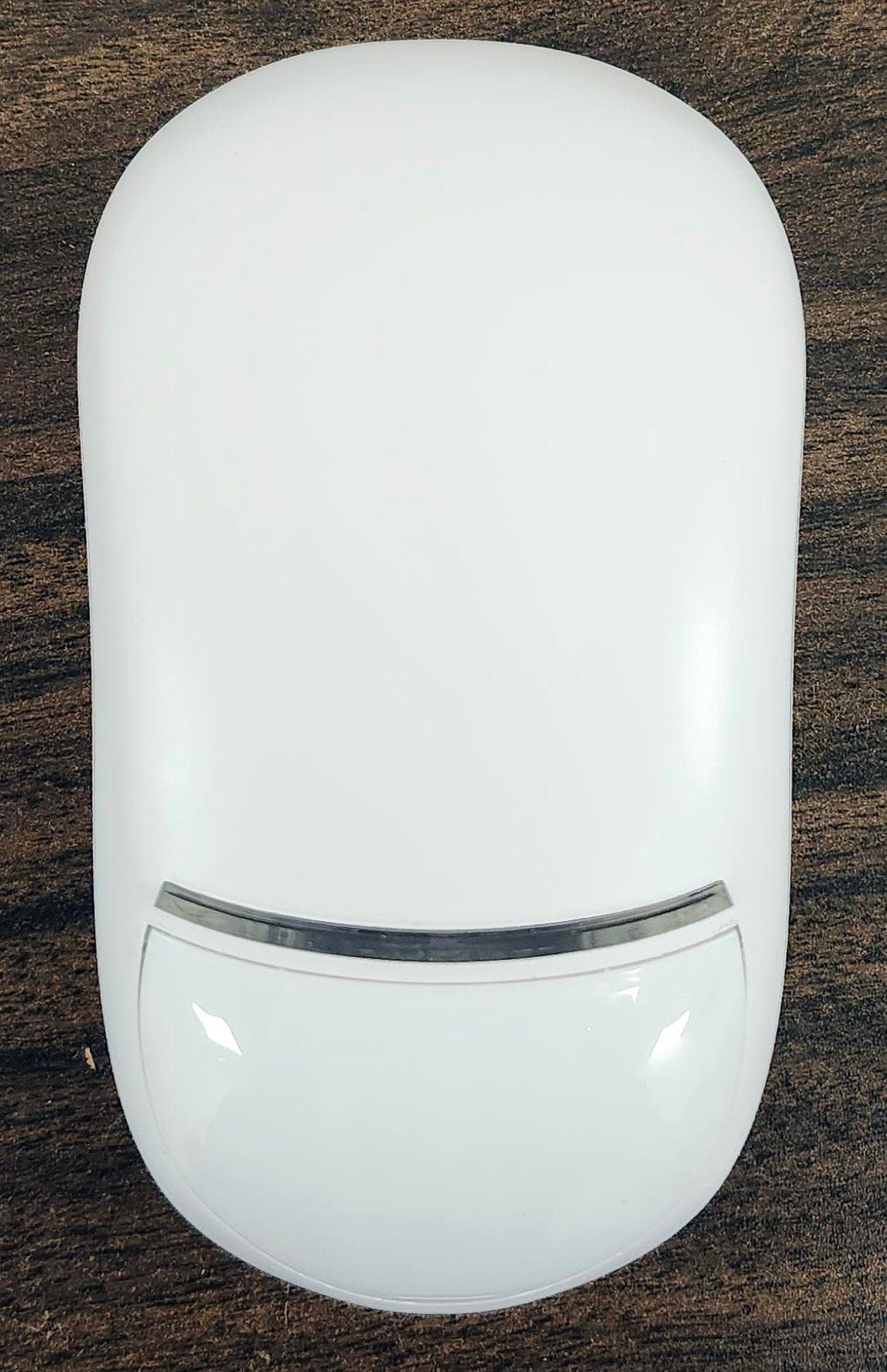
F5325LC203424
Dec 17, 2025Dual Technology Motion Sensor
Equipment Class
FDS - Part 15 Field Disturbance SensorF5324PGPIO9
Dec 04, 2024Wireless Input / Output (I/O) w/wo contact
Equipment Class
DSS - Part 15 Spread Spectrum Transmitter
F5323PGP9934P
Jan 16, 2024Wireless Motion detector with integrated camera
Equipment Class
DSS - Part 15 Spread Spectrum Transmitter