HE7ATGAsset Tag
Xmark Corporation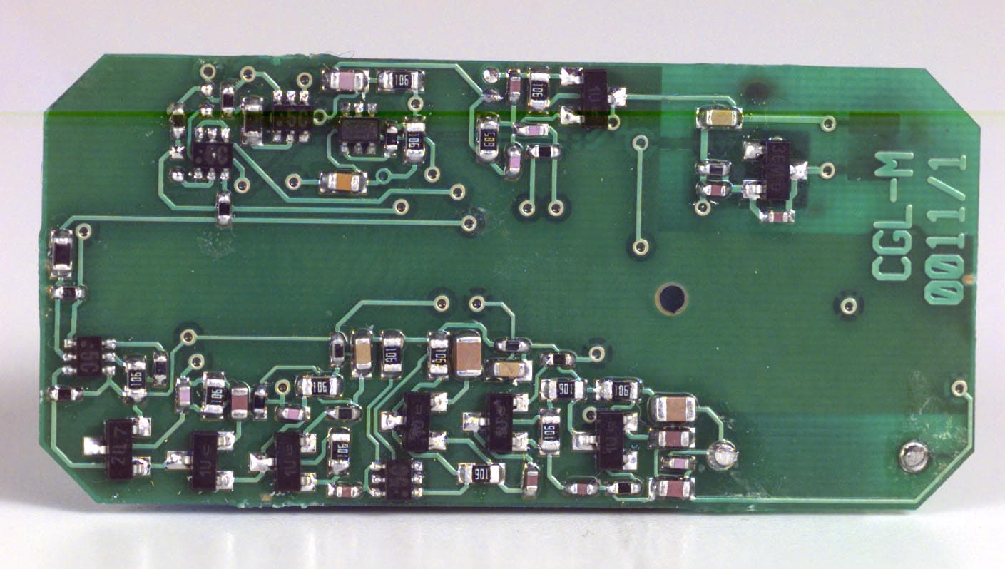
Click to zoom
Application Details
- Equipment Class
- DSC - Part 15 Security/Remote Control Transmitter
- Date of Grant
- Jun 21, 2000
- Application Purpose
- Original Equipment
- Date of Application
- Jun 12, 2000
- Equipment Note
- Asset Tag
- Frequency Range
- 433.92000000 - 433.92000000
- Company
- Xmark Corporation
- Country
- Canada
Documents & Files
Document Text
Text extracted from the exhibit documents filed with the FCC. Open a document above to read the original.
Users Manual
Revision 1.0 User Manual May 2000 © Copyright 2000, EXI Wireless Systems Inc. All rights reserved. EXI ASSETRAC User Manual980-000005-000 EXI Wireless Systems Inc.5May 2000 Revision 1.0 Table of Contents P 1.LIMITED WARRANTY ............................................................................................................3 P 2.RECORD OF CHANGES..........................................................................................................4 P 3.FCC REGULATIONS................................................................................................................5 P 4.SYSTEM MAINTENANCE.......................................................................................................6 1.SYSTEM INTRODUCTION..........................................................................................................9 1.1.SYSTEM COMPONENTS...............................................................................................................9 1.2.COMPUTER DISPLAY CONVENTIONS............................................................................................9 2.USER LEVEL...............................................................................................................................11 2.1.ENTERING AN ASSET................................................................................................................11 2.2.DELETING AN ASSET................................................................................................................14 2.3.SILENCING AND ACCEPTING ALARMS........................................................................................16 2.4.“STAFF SAVER” AND “LOITERING” FEATURES...........................................................................18 3.SUPERVISOR LEVEL................................................................................................................19 3.1.ACCESSING SUPERVISOR LEVEL................................................................................................19 3.2.EXITING SUPERVISOR LEVEL.....................................................................................................20 4.ACTIVITY LOG MANAGEMENT............................................................................................21 4.1.ACTIVITY LOGS.......................................................................................................................21 4.2.NAVIGATING THE ACTIVITY LOG...............................................................................................22 4.3.ADDING A SUPERVISOR ANNOTATION TO AN ALARM...................................................................22 4.4.BACKING UP ACTIVITY LOGS....................................................................................................23 5.MANAGING TAGS.....................................................................................................................24 5.1.TAGS.......................................................................................................................................24 5.2.ADDING A NEW ASSET-TAG TO THE SYSTEM..............................................................................25 5.3.DELETING AN ASSET-TAG FROM THE SYSTEM............................................................................26 5.4.DISABLING AN ASSET-TAG.......................................................................................................27 5.5.UNASSIGNING AN ASSET-TAG...................................................................................................27 5.6.EDITING AN ASSET-TAG RECORD..............................................................................................28 5.7.PRINTING.................................................................................................................................28 6.MANAGING SYSTEM USERS...................................................................................................29 6.1.ADDING A NEW USER TO THE SYSTEM........................................................................................30 6.2.DELETING A USER FROM THE SYSTEM........................................................................................31 6.3.DISABLING A SYSTEM USER.......................................................................................................31 6.4.EDITING A SYSTEM USER ACCESS...............................................................................................31 7.DEALER ONLY SCREEN..........................................................................................................32 7.1.ACCESSING THE DEALER LEVEL................................................................................................32 7.2.DEALER ACCESS LEVELS..........................................................................................................32 7.3.FLOOR PLAN EDIT....................................................................................................................33 7.4.ADDING SYSTEM DEVICES........................................................................................................34 8.SHUTTING AND RESTARTING THE SYSTEM......................................................................36 8.1.SHUTTING DOWN.....................................................................................................................36 8.2.RESTARTING THE SYSTEM.........................................................................................................36 EXI ASSETRAC User Manual980-000005-000 EXI Wireless Systems Inc.5May 2000 Revision 1.0 P 1. Limited Warranty EXI Wireless Systems Inc. (“EXI”) hereby warrants the product(s) accompanying this limited warranty (the “Product(s)”) to be free of defects in materials and workmanship for a period of two years (excluding any batteries that may be added to or used in conjunction with the Products(s)) from the date of delivery of the original purchase of the Produ…
Text truncated - open the document above for the full version.
ID Label/Location Info
Cases and markings Figure 1 illustrates the case design that will be used for the Asset tag. The diagram shows where the FCC identification will appear. e XI FCC ID: HE7 ATG Figure 1: Case and Markings for the Asset tag
Operational Description
Technical Memo TO: KTL FM: Chris Chattaway Date: June 14, 2000 Subject: Technical Description of the Halo Asset Tag Document Number: 970-000014-000 1 Introduction The purpose of this memo is to give a top-level technical description of the Asset tag. The Asset tag is used with the EXI Assetrac Asset protection system. The following sections describe the form and operation of the Asset tag. 2 Operation The Asset tag has two modes of operation, in field and tag initiated. First and foremost the Asset tag is an RF transceiver that receives a 307 KHz signal and replies with a 433.92 MHz signal. The tag upon entering a 307 KHz field wakes up and communicates its serial number to the controller (base station). The controller, over the 307 KHz field (channel), transmits wakeup and respond commands to the tag and also initiates and controls the serial number interrogation. The second mode of operation is initiated by the tag’s tamper circuitry. The tag is able to transmit to the nearest controller or receiver a message that indicates that the tag is being removed from the device it is protecting. This mode of operation is called Tag Initiated Communications (TIC). 2.1 In field Performance The Asset tag operates when in the 307 KHz field. When a tag enters the field it is prompted to power up by the wake up word that is transmitted by the controller (over 307 KHz field). Once powered up the tag will respond to the next wake up word with a 350μs pulse. This pulse prompts the controller to issue the serial number interrogation protocol command (bit by bit) and the serial number is extracted from the tag by the controller. Figure 1and Figure 2 illustrate this communication. The top traces show the output from the tag (433.92 MHz) and the bottom traces show the transmissions from the controller (307 KHz). The entire communication takes approximately 120ms (this time varies slightly from tag to tag based on the serial number). Figure 2 illustrates that the tag transmitter is working for approximately 80 ms of these 120 ms. For more information on the bit by bit protocol please refer to document “Bit-by-Bit Interrogation: Protocol Description” document number 970-000001-000. Now that the tag in the field is identified, the controller must periodically check to see if the tag is still in the field. Approximately every 12 sec. the tag will wake up and respond with a 350μs pulse when it sees the controller transmit a respond command. This communication is shown in Figure 3 and Figure 4. Figure 3 shows a bit by bit communication followed by a respond 11.47 seconds later and Figure 4 illustrates in detail the respond communication pulse. The respond communication will continue until the controller issues a reset command and re-interrogates all the tags in the field. The reset and re-interrogation occurs once per minute. Once again this behavior is detailed in the document “Halo communication Protocol” document number 970- 000002-000. Figure 1: Bit by Bit communication example 1 Figure 2: Bit by Bit communication example 2 Figure 3: Bit By Bit communication followed by first respond Figure 4: Respond Communication Example 2.2 TIC performance A TIC alarm is transmitted any time the tamper switch is closed. The switch protrudes from the bottom of the case and is intended to close when the tag is removed form the device it is protecting. Typically the tag will be adhered to a device and if the tag is tamper with or removed the switch will close. This switch closure powers up the tag and causes it to transmit its serial number to any/all controllers or receivers that are in range. The nature of the transmission is show n in Figure 5. This waveform shows that the transmitter is in use for approximately 48 ms (this var ies slightly wit h serial number). The transmitter will then t urn off for approximately 12 seconds and t hen, assuming the tamper switch is still closed, will transmit the signal show n in Figure 5 again. This sequence will continue with the time between TICs doubling each time as long as the tamper switch remains closed. Figure 6 and Figure 7 show three consecutive TIC transmissions and show the time between TICs 1 and two (13.59 sec.) and TICs 2and 3 (26.53 sec.) respectively. Figure 5: Waveform for single TIC Transmission Figure 6: TIC example - Time Between First and Second TIC Transmission Figure 7: TIC example - Time Between Second and Third TIC Transmission 3 Cases and markings Figure 8 illustrates the case design that will be used for the Asset tag. The diagram shows where the FCC identification will appear. e XI FCC ID: HE7 ATG Figure 8: Case and Markings for the Asset tag
Parts List/Tune Up Info
Item Qty. Ref. Part PCB Footprint Part #/man. Alt Part #/man. 1 1 A1 All capacitors are type NPO unless otherwise noted 2 1 A2 All resistors, capacitors, and inductors have 5% tolerances unless otherwise noted 3 1 A3 All capacitor voltages are 16v or greater unless otherwise noted 4 1 BT1 CR2032LF CR2032-SM same/Varta 5 3 C1,C2,C16 100n X7R SM/C_0603S 6 2 C13,C3 2.2n SM/C_0603S 7 2 C4,C5 47p SM/C_0402S 8 1 C6 8.2p sm/c_0402s 9 2 C7,C12 470p SM/C_0603S 10 1 C8 100p SM/C_0402S 11 1 C9 27p SM/C_0402S 12 1 C10 7-50p SM/4X4.5_TRM_CAP TZBX4R500AA110T00/Murata 13 1 C11 56p SM/C_0402S 14 1 C14 3.9p SM/C_0402S 15 1 C15 12p SM/C_0402S 16 1 C17 47n X7R SM/C_0603S 17 1 C18 820p SM/C_0603S 18 1 C19 1uF Tantlum SM/CT_3216_12S 19 2 C22,C20 10p SM/C_0402S 20 1 C21 33p SM/C_0402S 21 1 C23 220p sm/c_0402s 22 1 L1 1m AX/.375X.150/.031 CTC-0118-102/Coiltech 23 1 L2 22nH L_1008S 1008cs-220xjbc/Coilcraft 24 6 Q1,Q2,Q3,Q4,Q6,Q8 MMBT2484LT1 sm/sot23_123 same/motorola 25 1 Q5 MMBTH10LT1 SM/SOT23_123 same/motorola 26 1 Q7 MMBT5087LT1 sm/sot23_123 same/motorola 27 2 R1,R2 10k SM/R_0402S 28 15 R3,R4,R5,R6,R7,R9,R10, 10Meg SM/R_0603S R11,R14,R22,R23,R24,R26,R33,R36 29 8 R15,R21,R27,R31,R35,R37, 2.2Meg sm/r_0402s R38,R40 30 4 R16,R18,R28,R29 0 ohm SM/R_0402S 31 1 R19 100K SM/R_0402S 32 1 R20 820 ohm SM/R_0402S 33 1 R25 1.5Meg SM/R_0402S 34 2 R39,R30 4.75Meg 1% SM/R_0603S 35 1 R32 470k SM/R_0402S 36 1 R34 6.8Meg SM/R_0603S 37 1 SW1 Switch ASSET SWITCH N/A 38 4 U1,U2,U3,U5 MBT3946DW1T1 SM/SOT363 same/Motorola SMBT3904PN/Infineon 39 1 U4 MBT3906DW1T1 SM/SOT363 same/Motorola SMBT3906S/Infineon 40 1 U8 BU4093B SOG.65M/14/WG6.70/L5.20 BU4093BFV/Rohm 41 1 U10 CD4017BCM SOG.050/16/WG.244/L.400 Same/Fairchild MC14017BD/Motorola 42 1 U13 12C508-04/SM SOG.050/8/WG.330/L.225 same/Microchip 43 1 Y1 RO2101A - 433.92MHz RFM-SM2 Same/RFM 44 1 Y2 C-2 83.000KC-P CYL/D.075/LS.060/.020 Same/Epson America
Schematics
5 5 4 4 3 3 2 2 1 1 DD CC BB AA Note: Shielding is required between the RF and digital sections to ensure that high frequency components of the digital signals are not coupled into the receiver. A ground plane between the two circuits (layers) should be sufficient to provide this shielding. Design Notes: Revision Status: 1. Initial Halo compatible Asset tag release Jan. 2000 Component Notes: (These notes will appear in the BOM) Note: Components in the Tx section must be kept close to their respective ends of the antenna to ensure a working transmitter. In addition, traces connecting these componets should be of a width to avoid stray inductances. The grounds of C15, C16, and Y1 should be as physically close as possible, ideally a single point. Tx Section 911-000009-000RD1 Halo Asset Tag B 13Monday, January 17, 2000 Title SizeDocument NumberRev Date:Sheet of RF <Value> RD Vcc Gnd Rx Tx Digital <Value> Vcc Gnd Rx Tx RD Gnd Tx Vcc Rx RD A1 All capacitors are type NPO unless otherwise noted A2 All resistors, capacitors, and inductors have 5% tolerances unless otherwise noted A3 All capacitor voltages are 16v or greater unless otherwise noted
Schematics
5 5 4 4 3 3 2 2 1 1 DD CC BB AA Tx Section Note: Components in this section must be kept close to their respective ends of the antenna to ensure a working transmitter. In addition, traces connecting these componets should be of a width to avoid stray inductances. The grounds of C15, C16, and Y1 should be as physically close as possible, ideally a single point. 911-000009-000RD1 Halo Asset Tag RF Circuitry B 23Tuesday, March 14, 2000 Title SizeDocument NumberRev Date:Sheet of Rx_PWR1Vcc Gnd Rx_PWR2 Rx C16 100n X7R R18 0 ohm C8 100p R19 100K U1B MBT3946DW1T1 6 2 1 R20 820 ohm R14 10Meg C1 100n X7R C4 47p BT1 CR2032LF 1 2 C11 56p Q3 MMBT2484LT1 3 1 2 L1 1m R39 4.75Meg 1% C9 27p R7 10Meg C68.2p R4 10Meg L2 22nH C13 2.2n R10 10Meg R6 10Meg R11 10Meg Q1 MMBT2484LT1 3 1 2 Q5 MMBTH10LT1 3 1 2 Q4 MMBT2484LT1 3 1 2 R15 2.2Meg Q8 MMBT2484LT1 3 1 2 R38 2.2Meg R36 10Meg C3 2.2n R37 2.2Meg R16 0 ohm R9 10Meg R35 2.2Meg C5 47p R3 10Meg Q7 MMBT5087LT1 3 1 2 R40 2.2Meg U2A MBT3946DW1T1 3 5 4 R5 10Meg U2B MBT3946DW1T1 6 2 1 Q2 MMBT2484LT1 3 1 2 C7 470p U1A MBT3946DW1T1 3 5 4 C10 7-50p C15 12p C12 470p R1 10k R2 10k C23 220p C2 100n X7R Y1 RO2101A - 433.92MHz C14 3.9p Gnd Tx RD Rx Vcc
Schematics
5 5 4 4 3 3 2 2 1 1 DD CC BB AA 911-000009-000RD1 Halo Asset Tag Digital Circuitry B 33Monday, January 17, 2000 Title SizeDocument NumberRev Date:Sheet of Tx Rx_MP Rx Hold_Pwr RD Gnd Vcc U13 12C508-04/SM 1 2 3 7 6 5 4 8 VDD OSC1 OSC2 GP0 GP1 GP2 GP3 GND U8C BU4093B 9 8 10 R32 470k C21 33p C18 820p R31 2.2Meg C19 1uF Tantlum U5A MBT3946DW1T1 3 5 4 R34 6.8Meg R22 10Meg C17 47n X7R R26 10Meg R23 10Meg Y2 C-2 83.000KC-P R25 1.5Meg R30 4.75Meg 1% U10 CD4017BCM 14 13 15 3 2 4 7 10 1 5 6 9 11 12 16 8 CLK ENA RST Q0 Q1 Q2 Q3 Q4 Q5 Q6 Q7 Q8 Q9 CO VDD VSS U5B MBT3946DW1T1 6 2 1 R21 2.2Meg U4A MBT3906DW1T1 3 5 4 U8A BU4093B 1 2 7 14 3 U8B BU4093B 5 6 4 R29 0 ohm U4B MBT3906DW1T1 6 2 1 R27 2.2Meg R28 0 ohm SW1 Switch 12 InOut U3B MBT3946DW1T1 6 2 1 U3A MBT3946DW1T1 3 5 4 U8D BU4093B 13 12 11 C22 10p R24 10Meg R33 10Meg C20 10p Q6 MMBT2484LT1 3 1 2 Vcc Rx Tx RD Gnd
Schematics
5 5 4 4 3 3 2 2 1 1 DD CC BB AA Note: Shielding is required between the RF and digital sections to ensure that high frequency components of the digital signals are not coupled into the receiver. A ground plane between the two circuits (layers) should be sufficient to provide this shielding. Design Notes: Revision Status: 1. Initial Halo compatible Asset tag release Jan. 2000 Component Notes: (These notes will appear in the BOM) Note: Components in the Tx section must be kept close to their respective ends of the antenna to ensure a working transmitter. In addition, traces connecting these componets should be of a width to avoid stray inductances. The grounds of C15, C16, and Y1 should be as physically close as possible, ideally a single point. Tx Section 911-000009-000RD1 Halo Asset Tag B 13Monday, January 17, 2000 Title SizeDocument NumberRev Date:Sheet of RF <Value> RD Vcc Gnd Rx Tx Digital <Value> Vcc Gnd Rx Tx RD Gnd Tx Vcc Rx RD A1 All capacitors are type NPO unless otherwise noted A2 All resistors, capacitors, and inductors have 5% tolerances unless otherwise noted A3 All capacitor voltages are 16v or greater unless otherwise noted
Test Report
Master: ktlPT15231 Date: April 5, 2000 KTL Test Report:0R02527 Applicant:EXI Wireless Systems Inc. Suite 100-13551 Commerce Parkway Richmond, BC V6V 2L1 Equipment Under Test:ASSET TAG (E.U.T.) FCC ID:HE7 ATG In Accordance With:FCC Part 15, Subpart C For Low Power Transmitters Operating Periodically In The Band 40.66 - 40.77 MHz And Above 70 MHz Tested By:KTL Ottawa Inc. 3325 River Road, R.R. 5 Ottawa, Ontario K1V 1H2 Authorized By: R. Grant, Wireless Group Manager Date: Total Number of Pages:25 KTL Ottawa FCC PART 15, SUBPART C FOR LOW POWER TRANSMITTERS PROJECT NO.: 0R02527 EQUIPMENT: ASSET TAG FCC ID: HE7 ATG Page 2 of 23 Table of Contents Section 1. Summary of Test Results.......................................................................................... 3 Section 2. Equipment Under Test (E.U.T.) .............................................................................. 5 Section 3. Transmission Requirements .................................................................................... 6 Section 4. Occupied Bandwidth & Duty Cycle...................................................................... 15 Section 5. Periodic Alternate Field Strength Requirements................................................ 18 Section 6. Block Diagrams.......................................................................................................21 Section 7. Test Equipment List ................................................................................................ 23 Annex A Restricted Bands..................................................................................................... A1 KTL Ottawa FCC PART 15, SUBPART C FOR LOW POWER TRANSMITTERS PROJECT NO.: 0R02527 EQUIPMENT: ASSET TAG FCC ID: HE7 ATG Page 3 of 23 Section 1.Summary of Test Results General All measurements are traceable to national standards. These tests were conducted on a sample of the equipment for the purpose of demonstrating compliance with Part 15, Subpart C, Paragraph 15.231. All tests were conducted using measurement procedure ANSI C63.4-1992. Radiated emissions are made on an open area test site. A description of the test facility is on file with the FCC. New SubmissionProduction Unit Class II Permissive ChangePre-Production Unit D S CEquipment Code THIS TEST REPORT RELATES ONLY TO THE ITEM(S) TESTED. THE FOLLOWING DEVIATIONS FROM, ADDITIONS TO, OR EXCLUSIONS FROM THE TEST SPECIFICATIONS HAVE BEEN MADE. See “ Summary of Test Data”. NVLAP LAB CODE: 100351-0 TESTED BY: _____________________________________ DATE: ___________________ Kevin Carr, Technologist KTL Ottawa Inc. authorizes the above named company to reproduce this report provided it is reproduced in its entirety and for use by the company’s employees only. Any use which a third party makes of this report, or any reliance on or decisions to be made based on it, are the responsibility of such third parties. KTL Ottawa Inc. accepts no responsibility for damages, if any, suffered by any third party as a result of decisions made or actions based on this report. This report applies only to the items tested. KTL Ottawa FCC PART 15, SUBPART C FOR LOW POWER TRANSMITTERS PROJECT NO.: 0R02527 EQUIPMENT: ASSET TAG FCC ID: HE7 ATG Page 4 of 23 Summary Of Test Data Name of TestPara. NumberResults Transmission Requirements15.231(a)Complies Radiated Emissions15.231(b)Not Applicable Occupied Bandwidth15.231(c)Complies Frequency Tolerance15.231(d)Not Applicable Periodic Alternate Field Strength Requirements15.231(e)Complies Powerline Conducted Emissions15.207Not Applicable Footnotes For N/A’s: – Applicant filing under Clause 15.231(e) – Applicant does not transmit within the band specified by Clause 15.231(d) Test Conditions: Indoor Temperature: 24 °C Humidity:35 % Outdoor Temperature: 24 °C Humidity:35 % KTL Ottawa FCC PART 15, SUBPART C FOR LOW POWER TRANSMITTERS PROJECT NO.: 0R02527 EQUIPMENT: ASSET TAG FCC ID: HE7 ATG Page 5 of 23 Section 2.Equipment Under Test (E.U.T.) General Equipment Information Manufacturer: EXI Wireless Systems Inc. Model No.: ASSET TAG Serial No.: None Date Received In Laboratory: May 25, 2000 KTL Identification No.: Item #1 Frequency Range: 434 MHz Operating Frequency(ies) of Sample: 433.9 MHz Type of Emission: PCM Emission Designator: 66K7L1D Supply Power Requirement: Battery Duty Cycle Calculation: 20 Log + 100 5.0435.025 xx = -19.4dB KTL Ottawa FCC PART 15, SUBPART C FOR LOW POWER TRANSMITTERS PROJECT NO.: 0R02527 EQUIPMENT: ASSET TAG FCC ID: HE7 ATG Page 6 of 23 Section 3.Transmission Requirements Para. No.: 15.231(a) Test Performed By: Kevin Carr Date of Test: June 6, 2000 Minimum Standard: 15.231(a) Continuous transmissions such as voice, video or data transmissions are not permitted. 15.231(a)(1) A manually operated transmitter shall employ a switch that will automatically deactivate the transmitter within not more than 5 seconds after being released. 15.231(a)(2) A transmitter activated automatically shall cease transmission within 5 seconds of activation. 15.231(a)(3) Periodic transmissions at regular pre-determined intervals are not permitted. However polling or supervisory transmissions to determine system integrity of transmitters used in security or safety applications are allowed if the periodic rate of transmission does not exceed one transmission of not more than one second duration per hour for each transmitter. 15.231(a)(4) Intentional radiators which are employed for radio control purposes during emergencies involving fire, security, and safety of life, when activated to signal an alarm, may operate during the pendency of the alarm. Test Results: Complies. Test Data: Compliance was determined by verification of technical specifications and a functional test on the equipment. KTL Ottawa FCC PART 15, SUBPART C FOR LOW POWER TRANSMITTERS PROJECT NO.: 0R02527 EQUIPMENT: ASSET TAG FCC ID: HE7 ATG Page 7 of 23 Rationale for Compliance with Transmission Requirements 15.231(a)(1) : The E.U.T. is…
Text truncated - open the document above for the full version.
Contact Information
Applicant
Chris Bisaillion(Senior RF Designer)
Technical Contact
Non-Technical Contact
KTL Ottawa Inc.Ruby C Dulmage
[email protected]800-563-6336
Test Firm
Nemko Canada Inc.Stuart Beck
Technical Specifications
| # | Rule Parts | Frequency Range | Power Output |
|---|---|---|---|
| 1 | 15C | 433.92 MHz - 433.92 MHz | - |
Other Applications from Xmark Corporation
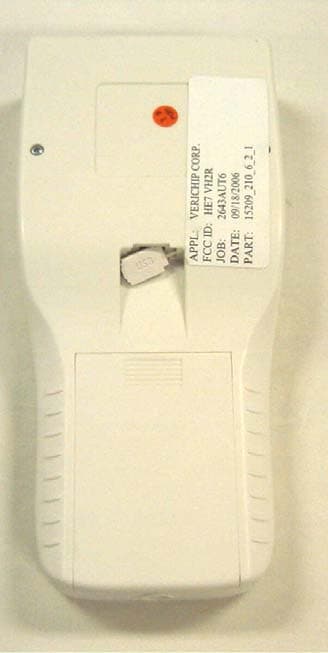
HE7VH2R
Oct 18, 2006VERICHIP H2 READER
Equipment Class
DXX - Part 15 Low Power Communication Device Transmitter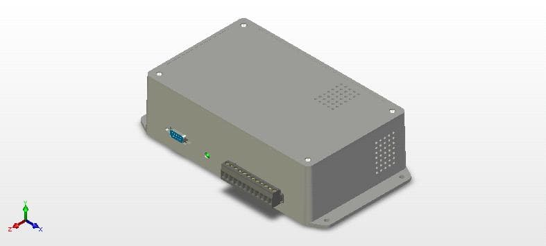
HE7VACR
May 21, 2006VERIGUARRD ACCESS CONTROL READER
Equipment Class
DXX - Part 15 Low Power Communication Device Transmitter
HE7PCR
Apr 06, 2005Receiver
Equipment Class
CYY - Communications Receiver used w/Pt 15 Transmitter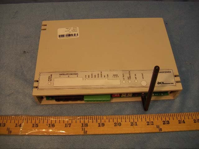
HE7EAC
Feb 07, 2005Transceiver
Equipment Class
DCD - Part 15 Low Power Transmitter Below 1705 kHz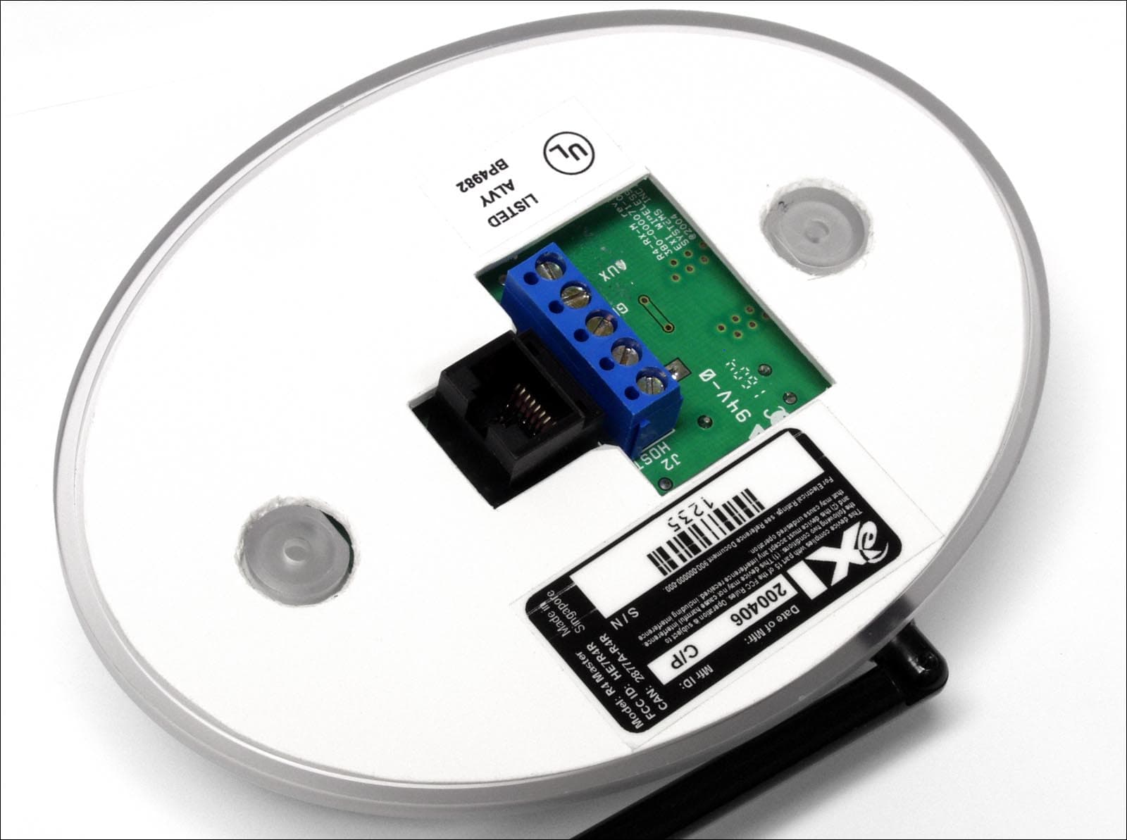
HE7R4R
Oct 13, 2004Communications Receiver
Equipment Class
CYY - Communications Receiver used w/Pt 15 Transmitter