HE7VH2RVERICHIP H2 READER
Xmark Corporation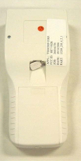
Click to zoom
Application Details
- Equipment Class
- DXX - Part 15 Low Power Communication Device Transmitter
- Date of Grant
- Oct 18, 2006
- Application Purpose
- Original Equipment
- Date of Application
- Oct 18, 2006
- Equipment Note
- VERICHIP H2 READER
- Frequency Range
- 0.13420000 - 0.13420000
- Company
- Xmark Corporation
- Country
- Canada
Documents & Files
Document Text
Text extracted from the exhibit documents filed with the FCC. Open a document above to read the original.
Users Manual
OPERATOR’S MANUAL AN APPLIED DIGIT AL COMPANY 21 USER INSTRUCTIONS Description The VeriChip H2 Reader is hand-held Radio Frequency Identification (RFID) reader which activates an implanted VeriMed™ RFID Microtransponder with a low power, low frequency (LF) electromagnetic field. The Reader receives a unique 16-digit ID number from the VeriMed Microtransponder. The ID number is used to provide, with patient consent, physicians and other health professionals access to a secure database that will provide the implanted person’s identity and health information provided by the patient. Indications The VeriChip H2 Reader is indicated for use as a portable instrument that non-invasively reads the ID number of an implantable VeriMed Microtransponder that is inserted into the arm of the patient. When activated, the VeriMed Microtransponder transmits a unique identification number that will be displayed by the VeriChip H2 Reader and may be used to access the patient’s identity and authorized health information from a secure database. Contraindications None. Contents:VeriChipH2 Reader Assembly Part Number 600-000515-000 (includes all of the following): VeriChip H2™ Reader Activation with Manufacturer Settings 1. Press Button F1 and release to power on the Reader. 2. The Reader will enter a self diagnostic mode displaying the following on the LCD screen: a. “Initializing” b. “VeriChip H2 Reader” “BT Master Rev x.xx” c. All Pixels active on the two line screen display d. The number “8” will display in all positions Check for missing segments. If segments are missing, do not use and r eturn Reader immediately for repair or replacement. e. “Battery OK” f. “BT Connecting - Inquiry Done - Please Wait” 3. Screen will display “PRESS F1 TO SCAN” 4. Press the F1 button and “SCANNING” will be displayed. 5. Perform the scanning process as described on page 3. 6. When a V eriMed ID number is f ound, an audible chirp will be heard and the VeriMed ID number will be displayed on the top line of the LCD and on the second line the ins truction “PRES S F1 TO SCAN” is displayed. To initiate a new scan session press F1 again. To scan for a different VeriMed Microtransponder press the F1 button t o cl ear the pr e vious ID number and to restart the scanning mode. DescriptionPart Number VeriChip H2 Reader (1)600-100313-000 with lanyard and instruction card attached Instructions for Use (1)981-000302-000 Batteries AA (1 set of 4)303-000014-000 Test Microtransponder (1)670-000001-000 Bluetooth Receiver (1) 672-000001-000 with related Driver CD (1) Folder Poster (1)420-000025-000 Instructional CD (1)672-000002-000 USB Cable (1)301-000025-000 34 Prior to Scanning Patient Scan test Microtransponder provided with VeriChip H2 Reader to verify unit functionality prior to use (photo) . . Sc anning Procedure for Loc ating an Implanted VeriMed Microtransponder To scan/locate a Microtransponder first activate the Reader as described above. Press and release the F1 button when instructed on the LCD. DO NOThold down F1 button during scan operation. Place the Reader next to the skin, parallel and along side the area to be scanned (see photo). Starting about 2 inchesabove the elbow, move the scanner slowly up the rear part of the arm. The injection site may vary but it typically will be between the elbow and shoulder of the triceps area of the upper arm. When a VeriMed Microtransponder is located, the VeriChip H2 Reader will emit an audible chirp and display the 16-digit ID number on the LCD screen. Depending on which communication configuration is established, the VeriMed ID number will be entered via USB or Bluet ooth int o the designat ed entry field in the web enabled VeriMed Patient Registry. If no communication is es tablished, the PC keyboard can be used to manually enter the ID number. Turning the Reader Off The Reader can be turned off manually at any time by simultaneously pressing and holding down the F2 and F3 buttons. If the Authorization Code is enabled and an incorrect Authorization Code be entered, the unit will immediately power-off. The Reader will automatically power down should it remain idle for 5 minutes. Use of VeriMed Reader with Passive Microtransponders of Different RFID Frequencies The VeriMed H2 Reader is capable of reading the VeriMed Microtransponder frequency of 134.2 kHz as well as 125 KHz. Place the Reader within the effective range of the passive RFID Microtransponder (no more than 2.5 inches) to obtain the ID number from the Microtransponder. Installing/Replacing the Batteries Remove the battery compartment door by pressing the tab and sliding towards the base of the Reader case. Insert 4 AA alkaline batteries into the battery compartment as indicated (see photo). Replace the battery compartmentcover and test the Reader using the provided test RFID Microtransponder. When the Reader battery power level drops to a point insufficient to read a VeriMed Microtransponder the Reader will automatically shut off. The Reader will display “LOW BATTERY” followed by “REPLACE BATTERY”. When these messages appear on the LCD, replace batteries immediately. 8756 Authorization Code Option To provide a means of securing the VeriMed H2 Reader against unauthorized use, an optional start-up Authorization Code function is provided. This modality consists of 8 entries of the two auxiliary buttons, F2 (left) and F3 (right) in a predefined sequence. The factory default setting is ‘disabled’, i.e. the unit will not prompt the user to enter an Authorization Code, but rather will immediately proceed to scan mode and establishing a link with the host computer. This feature can be enabled or disabled through the Configuration Mode (see configuration mode section below). If enabled, the Authorization Code is entered after the Reader is turned on and self-tests are complete. The user must press the two auxiliary buttons a total of 8 times in predefined sequence. This sequence can be customized and stored in the EEPROM. The default sequ…
Text truncated - open the document above for the full version.
Block Diagram
55 44 33 22 11 D D C C B B A A 3.3V 3.3V 3.3V 3.3V TitleSize Document Number Rev Date: Sheet of 912-000xxx-000 1.00 VH2R - Block Diagram C 1 1 Monday, October 02, 2006 TitleSize Document Number Rev Date: Sheet of 912-000xxx-000 1.00 VH2R - Block Diagram C 1 1 Monday, October 02, 2006 TitleSize Document Number Rev Date: Sheet of 912-000xxx-000 1.00 VH2R - Block Diagram C 1 1 Monday, October 02, 2006 DriverRectifier BANDPASSFILTER &LIFIER 134.2kHz BASEBAND PROTECTIONCIRCUIT VOLTAGEREGULATORIN OUTON/OFF KEYPADINTERFACE &PROTECTIONCIRCUIT SYSTEM MICROCONTROLLER KEYPAD BUS SYSTEMCLOCK USBTRANSCEIVER USBCONNECTORBLUETOOTHTRANSCEIVERMODULE DATASWITCH UART DATA BUS COMMUNICATION CHANNEL SELECT ANTENNAASSEMBLY COMPARATORINPUT PWMOUTPUT LCDMODULE LCD BUS BACKLIGHT BACKLIGHTDRIVER ON/OFF OUT BATTERYSTATUS A/D INPUT DIGITAL OUTPUT DIGITAL OUTPUTDIGITAL OUTPUT DIGITAL OUTPUTUART I/ODIGITAL INPUT Driver INTERFACE BOARD KEYPADASSEMBLY Power Supply (AA alkaline Batt. x 4) BT16V BATTERYBT16V BATTERY L1EXCITER COILL1EXCITER COIL LS1BUZZERLS1BUZZER SW 2 F2 SW 2 F2 L2RECEIVER COILL2RECEIVER COIL SW 1 F1 SW 1 F1 L3RECEIVER COILL3RECEIVER COIL SW 3 F3 SW 3 F3 Y1CRYSTALY1CRYSTAL
External Photos
APPLICANT: VERICHIP CORP. MODEL: HE7VH2R REPORT: V\VERICHIP\2643AUT6
ID Label/Location Info
FCC and Industry Canada Label Sample – Fit to Device Proposed Label Location - Back Side of DUT Verichip Manufacturer Verichip Corporation Model: Verichip H2 Reader FCC ID: HE7VH2R IC: 2877A-VH2R This device complies with part 15 of the FCC rules. Operation is subject to the following two conditions: (1) This device may not cause harmful interference, and (2) this device must receive any interference received, including interference that may cause undesired operation. Serial No. xxxxxx Made in Canada
Internal Photos
DUT Internal Photos
Operational Description
VeriChip H2 Reader (VH2R) -Theory of Operation Document Number: 900-100000-015 Project Number: 2005-12 Revisions Revision Date Changed by Description 1.00 Oct 3, 2006 F. Chow Initial Release VH2R Theory of Operation Refer to schematic diagram 911-000090-000. VH2R is a handheld, battery-operated device for reading the implantable passive RFID chips manufactured according to ISO 11784 and ISO 11785 (134.2kHz, FDX). The device performs generating the activation magnetic field, receiving and decoding the ASK field modulation signal produced by the chip, validating the received telegram, extracting the identification code, converting the identification code into BCD format, displaying the identification code on the built-in LCD and sending the identification code to a host computer system by means of either wireless Bluetooth connection or USB (full speed) connection. Activation field generation is performed by the Transmit Antenna coil connected to the single-ended power amplifier Q3 through a resonant network comprised of C16, C17, R20, and R44. Capacitors C18 and C44 may be installed during manufacturing tuning. The power amplifier MOSFET Q3 is driven by the PWM signal produced by the microcontroller U1. Receiving the field modulation signal from the chip is performed by the two receive antenna coils connected in counter-phase to suppress external noise. The receive antenna is tuned to resonance during manufacturing by the set of fixed tuning capacitors C45, C46, C47 that can be connected to the tank by means of solder jumpers S1, S2, S3. The signal picked up by the coils is passed through the diode demodulator D2. The high frequency (134.2 kHz) carrier is filtered out by the demodulator load/filter network C29, R34, R25, C32. The low frequency component is passed to the active low pass filter designed around U3A, U3B, and U3D. The switch U10 is used to mute the receiver when the activation field is just turned on and ramps up. This reduces filter overload by the strong transient that is produced when the activation field is turned on and shortens the recovery time of the whole receiver. Filtered baseband signal is applied to one input (pin 10) of the analog comparator inside the system microcontroller U1. The second input of the comparator receives the same baseband signal, but heavily filtered by the low pass filter R18, C20. This filter tracks the signal baseline, but almost completely suppresses the useful data modulation. As the result, the comparator output (not accessible outside the microcontroller) produces the digitized data modulation signal. The data produced by the comparator is continuously sampled by the microcontroller’s firmware. When an identification telegram that complies with the requirements of ISO 11785 Standard is received, its validity is checked by comparing the received 16-bit CRC checksum with the one calculated by the microcontroller. If the message is found valid, the microcontroller extracts the identification code and re-formats it from binary to BCD format. The message is then sent to the local LCD. The LCD is connected to the microcontroller in 4-bit write-only mode. The LCD has a temperature-compensated contrast adjustment circuit R2, R3, R5. The LCD also has internal backlight driven by the constant current sink Q2. The current sink provides constant backlight brightness throughout the whole battery voltage range (from 6.4V for a set of fresh alkaline cells down to 4.0V at the end of their useful life). The backlight circuit is also used for battery voltage monitoring. The voltage drop at the resistor R11 is measured by the microcontroller’s ADC. The circuit parameters are selected in such a way that when the battery approaches the end of its life, the current sink starts dropping out of compliance, and the voltage across R11 starts decreasing rapidly. The firmware compares the voltage with a certain threshold programmed into the non-volatile memory during manufacturing process and is then able to detect when the battery voltage drops below the pre-defined value. The low battery threshold of 4.0V allows use of both primary alkaline cells and rechargeable NiCd and NiMH cells. The reader has a buzzer BZ1 used for audible indication of various processes such as power-up and chip detection. The buzzer is of self-oscillating type and is controlled by a DC signal (pulse) from the microcontroller via the transistor Q4. Communication interface of the reader consist of two devices, the USB-to-UART chip U9 and the Bluetooth module U6. Since the microcontroller has single UART channel, only one of the two possible interfaces can be used at a time. The selection is performed by the data switch U8 depending on the desired mode of operation which is stored in the non-volatile memory of the microcontroller and recalled during start-up. The data switch is controlled by pin 2 (PD4) of the microcontroller, its high state corresponds to USB interface, and low – to Bluetooth. The communication modules are serviced by a separate reset chip U7. Resistors R49 and R50 are used to select the required polarity of the reset signal to the Bluetooth module depending on the latter’s version. Power management system consists of the LDO regulator U2, input protection devices D8 and F1 and power hold network built around Q1. When the F1 button is first pressed, the Q1 turns on via R42 and lower part of dual diode D1. This turns on the LDO regulator U2 that produces 3.3V for the microcontroller. The latter starts up and asserts its pin 13 (PB1) high. This signal is applied through the diode D5 to the control input of the LDO and thus the power is now maintained even when user releases the button F1. The user can press and release the F1 button any time after that and the switch status will be read by the microcontroller through the upper part of the dual diode D1. Keypad interface consists of three inputs protected with ESD/EMI suppression chips Z1- Z3. Keypad inputs are active low (the …
Text truncated - open the document above for the full version.
Schematics
55 44 33 22 11 D D C C B B A A UART-RX BEEPER RESET UART-TX RESET LCD-D7 BUTTON3 LCD-E 134.2kHzUSB/nBT LCD-RS BATT-MONRX-BLANK 134.2kHz LCD-E LCD-BL BUTTON1 PWR-HOLD BUTTON2 BT-CONNECTED LCD-D4 LCD-D5 LCD-D6 LCD-D4LCD-D5LCD-D6LCD-D7LCD-RS BEEPER BT-CONNECTED USB/nBTUART-TXUART-RX BUTTON1 BATT-MON RX-BLANK BUTTON3BUTTON2 PW R-HOLD +1.1V +1.1V +1.1V +3.3V +3.3V +3.3V +3.3V +3.3V +3.3V +3.3V +3.3V +1.1V +3.3V +3.3V +3.3V TitleSize Document Number Rev Date: Sheet of 911-000090-000 2.00 VeriMed Handheld Reader - Main Board C 1 2 Thursday, August 31, 2006 TitleSize Document Number Rev Date: Sheet of 911-000090-000 2.00 VeriMed Handheld Reader - Main Board C 1 2 Thursday, August 31, 2006 TitleSize Document Number Rev Date: Sheet of 911-000090-000 2.00 VeriMed Handheld Reader - Main Board C 1 2 Thursday, August 31, 2006 ISP P10536CT-ND InterfaceBoard Keypad BatteryTerminals TransmitAntenna ReceiveAntenna Bourns Molex/Waldom B32621A5473JEPCOS B37641K7475K62 Confidential, unpublished property of VeriChip Syst ems Inc. Distribution limited solely to authorized personnel . R5 TC03X-2-103E R5 TC03X-2-103E 13 2 C44100pF* 500VC44100pF* 500V +- U3CLMC6484 +- U3CLMC6484 1213 14 D5MMSD914T1D5MMSD914T1 C522pFC522pF D4MBRS140T3D4MBRS140T3 Z2 TransFeed Z2 TransFeed R44 10R 0.5W R44 10R 0.5W D8SMBJ10AD8SMBJ10A L247uHL247uH C32560pFC32560pF R35 33KR35 33K R29820KR29820K C1747nFC1747nF C24100nFC24100nF R433KR433K C256.8nFC256.8nF C30150pFC30150pF R1510KR1510K R10 2K0R10 2K0 C333.3nFC333.3nF D6 MMSD914T1 D6 MMSD914T1 J1 22-28-8083 J1 22-28-8083 1234 C46150pFC46150pF C37100nFC37100nF R121K2R121K2 C3147pFC3147pF C210uF 10VC210uF 10V R333K3R333K3 R710KR710K Y1 11.059MHzY1 11.059MHz Z1 TransFeed Z1 TransFeed R22DNPR22DNP R4210KR4210K C1410nFC1410nF R1610KR1610K M10M-HoleM10M-Hole 1 1 S2 SolderBridge S2 SolderBridge J4 CON8 J4 CON8 12345678 R193K3R193K3 M9M-HoleM9M-Hole 1 1 C1 10nF C1 10nF D2MMSD914T1D2MMSD914T1 R8510RR8510R C353.3nFC353.3nF +- U3A LMC6484 +- U3A LMC6484 32 1 Q1MMBT3906Q1MMBT3906 R322K2R322K2 C291nFC291nF TP1+3.3VTP1+3.3V M2M-HoleM2M-Hole 1 1 R37 10KR37 10K C163.9nF 400VC163.9nF 400V R24100KR24100K M8M-HoleM8M-Hole 1 1 C1210uF 10VC1210uF 10V J3PTC3DAANJ3PTC3DAAN 123456 R289K1R289K1 Q3 FDN337N Q3 FDN337N TP10 ANT-RX-GND TP10 ANT-RX-GND U2 LP2992 U2 LP2992 Vin 1 GND 2 ON/OFF 3 Bypass 4 Vout 5 J2 LCD-LM4047 J2 LCD-LM4047 NC 1 NC 2 Vss 3 Vdd 4 Vo 5 RS 6 R/W 7 E 8 D0 9 D1 10 D2 11 D3 12 D4 13 D5 14 D6 15 D7 16 LED+ 17 LED- 18 Vee 19 NC 20 TAB1 21 TAB2 22 M7M-HoleM7M-Hole 1 1 C1010nFC1010nF M3M-HoleM3M-Hole 1 1 R271K8R271K8 TP5RXTP5RX C13100nFC13100nF C9100nFC9100nF R18100KR18100K TP8ANT-TX-GNDTP8ANT-TX-GND R23100KR23100K R6100KR6100K TP7ANT-TXTP7ANT-TX TP2BAT+TP2BAT+ C15100uF 10VC15100uF 10V C4910nFC4910nF C610uF 10VC610uF 10V C47100pFC47100pF C410nFC410nF C191.5nFC191.5nF S3 SolderBridge S3 SolderBridge L1BLM21PG221SN1DL1BLM21PG221SN1D F1MF-NSMF-050-2F1MF-NSMF-050-2 R20 10R 0.5W R20 10R 0.5W R2510KR2510K U1 ATMEGA168-TQFP U1 ATMEGA168-TQFP RESET PC6 29 (RXD) PD0 30 (TXD) PD1 31 (INT0) PD2 32 (OC2B/INT1) PD3 1 (XCK/T0) PD4 2 Vcc 4 GND 3 (XT1/TOSC1) PB6 7 (XT2/TOSC2) PB7 8 (OCOB/T1) PD5 9 (OC0A/AIN0) PD6 10 (AIN1) PD7 11 (CLK0/ICP) PB0 12 (OC1A) PB1 13 (SS/OC1B) PB2 14 (MOSI/OC2) PB3 15 (MISO) PB4 16 PB5 (SCK) 17 AVCC 18 AREF 20 ADC7 22 PC0 (ADC0) 23 PC1 (ADC1) 24 PC2 (ADC2) 25 PC3 (ADC3) 26 PC4 (ADC4/SDA) 27 PC5 (ADC5/SCL) 28 GND 5 Vcc 6 ADC6 19 GND 21 R17 10RR17 10R +- U3B LMC6484 +- U3B LMC6484 56 7 R21 1K8 R21 1K8 M4M-HoleM4M-Hole 1 1 C1110nFC1110nF R1112RR1112R C310nFC310nF R4615KR4615K TP4BAT-TP4BAT- C22 10uF 10V C22 10uF 10V R34390KR34390K C504.7uFC504.7uF C18300pF* 500VC18300pF* 500V R369K1R369K1 M1M-HoleM1M-Hole 1 1 C21100nFC21100nF C722pFC722pF TP9 ANT-RX TP9 ANT-RX C363.3nFC363.3nF R2 ERT-J1VT102J R2 ERT-J1VT102J Z3 TransFeed Z3 TransFeed R3010KR3010K Q2 MMBT3904 Q2 MMBT3904 D1BAV70LT1GD1BAV70LT1G 12 3 C20100nFC20100nF R31 11KR31 11K C261800pFC261800pF C28100pFC28100pF C45220pFC45220pF U10 NC7SZ66M U10 NC7SZ66M A 1 B 2 GND 3 OE 4 VCC 5 R31K5R31K5 C23100nFC23100nF R5210KR5210K C810uF 10VC810uF 10V S1 SolderBridge S1 SolderBridge R933KR933K -+ U3DLMC6484 -+ U3DLMC6484 10 9 8 411 R1333KR1333K R110KR110K 55 44 33 22 11 D D C C B B A A SCI-RXSCI-TX BT-CONNECT BPRUSB-BTSYSGND3.3Vdd B+ TitleSize Document Number Rev Date: Sheet of 911-000090-000 2.0 VeriMed Handheld Reader - Interface Board B 2 2 Thursday, August 31, 2006 TitleSize Document Number Rev Date: Sheet of 911-000090-000 2.0 VeriMed Handheld Reader - Interface Board B 2 2 Thursday, August 31, 2006 TitleSize Document Number Rev Date: Sheet of 911-000090-000 2.0 VeriMed Handheld Reader - Interface Board B 2 2 Thursday, August 31, 2006 BR-C30ABR-C40A Confidential, unpublished property of VeriChip Syst ems Inc. Distribution limited solely to authorized personnel . TP20 GP1TP20 GP1 R5133KR5133K R4310KR4310K TP15 DTRTP15 DTR M11M-HoleM11M-Hole U9CP2103U9CP2103 RI 1 GND 2 D+ 3 D- 4 Vio 5 Vdd 6 REGin 7 VBUS 8 RST 9 NC 10 SUSPEND 11 SUSPEND 12 NC 13 NC 14 NC 15 GPIO3 16 GPIO2 17 GPIO1 18 GPIO0 19 NC 20 NC 21 CTS 22 RTS 23 RXD 24 TXD 25 DSR 26 DTR 27 DCD 28 GND 29 GND 30 TP21 GP2TP21 GP2 R380RR380R C42 100nFC42 100nF C39 100nFC39 100nF TP22 GP3TP22 GP3 Q4MMBT3904Q4MMBT3904 M6M-HoleM6M-Hole 1 1 U7 TPS3825 U7 TPS3825 MR 4 GND 2 RESET 3 RESET 1 Vdd 5 TP14 DSRTP14 DSR C38 10uF 10VC38 10uF 10V TP24P7TP24P7 U874HC4053U874HC4053 X0 12 X1 13 Y0 2 Y1 1 Z0 5 Z1 3 EN 6 X 14 Y 15 Z 4 VCC 16 GND 8 VEE 7 A 11 B 10 C 9 TP17 NSUSTP17 NSUS Q5 MMBT3904 Q5 MMBT3904 TP18 SUSTP18 SUS D3uESD5.0DT5GD3uESD5.0DT5G 1 2 3 TP25 P5 TP25 P5 TP26P3TP26P3 R49 0R R49 0R U6 BR-C40A U6 BR-C40A GND 1 SPI_MOSI 2 PIO[6] 3 PIO[7] 4 RESET 5 SPI_CLK 6 PCM_CLK 7 PCM_SYNC 8 PCM_IN 9 PCM_OUT 10 Vdd 11 GND 12 UART_RX 13 UART_TX 14 UART_RTS 15 UART_CTS 16 _ 17 _ 18 PIO[2] 19 PIO[3] 20 PIO[5] 21 PIO[4] 22 SPI_CSB 23 SPI_MISO 24 GND 25 NC 26 GND 27 GND 28 GND 29 R392K2R392K2 R4010KR4010K J5CON8J5CON8 12345678 C27100nFC27100nF TP13 TRSTP13 TRS TP23P6TP23P6 M13M-HoleM13M-Hole R4533KR4533K R2610KR2610K …
Text truncated - open the document above for the full version.
Test Report
FCC PART 15.209 LOW POWER UNLICENSED INTENTIONAL RADIATOR TEST REPORT Applicant VERICHIP CORP. Address 13551 COMMERCE PARKWAY SUITE 100 RICHMOND BRITISH COLUMBIA V6V 2L1 CANADA FCC ID HE7VH2R Model Number VH2R Product Description 135 kHz Handheld Transmitter Date Sample Received 9/18/2006 Date Tested 9/21/2006 Tested By Richard Block Approved By Mario de Aranzeta Report Number 2643AUT6TestRepot Test Results PASS FAIL THE ATTACHED REPORT SHALL NOT BE REPRODUCED EXCEPT IN FULL WITHOUT THE WRITTEN APPROVAL OF TIMCO ENGINEERING, INC. 849 NW State Road 45 Newberry, FL 32669 USA Phone: 888.472.2424 or 352.472.5500 Fax: 352.472.2030 Email: [email protected] Website: www.timcoengr.com Certificate # 0955-01 Applicant: Verichip Corp. FCC ID: HE7 VH2R Report:V:\V\VERICHIP\2643AUT6\2643AUT6TestReport.doc Page 2 of 10 TABLE OF CONTENT STATEMENT OF NON COMPLIANCE.......................................................................... 3 GENERAL INFORMATION .......................................................................................... 4 EMC EQUIPMENT LIST ............................................................................................. 5 TEST PROCEDURES ................................................................................................. 6 RADIATION INTERFERENCE ..................................................................................... 7 OCCUPIED BANDWIDTH ........................................................................................... 8 POWER LINE CONDUCTED INTERFERENCE............................................................. 9 Applicant: Verichip Corp. FCC ID: HE7 VH2R Report:V:\V\VERICHIP\2643AUT6\2643AUT6TestReport.doc Page 3 of 10 STATEMENT OF COMPLIANCE Certificate #0955-01 This equipment has been tested in accordance with the standards identified in the referenced test report. To the best of my knowledge and belief, these tests were performed using the measurement procedures described in this report and demonstrate that the equipment does comply with the appropriate standards. I attest that the necessary measurements were made by me or under my supervision, at TIMCO ENGINEERING, INC. located at 849 N.W. State Road 45, Newberry, Florida 32669 USA. Authorized by: Mario de Aranzeta Signature: Function: Engineer Date: 9/25/2006 Tested by: Richard Block Signature: on file Date: 9/21/2006 Applicant: Verichip Corp. FCC ID: HE7 VH2R Report:V:\V\VERICHIP\2643AUT6\2643AUT6TestReport.doc Page 4 of 10 GENERAL INFORMATION Disclaimer The test results relate only to the items tested. Applicable Standards FCC CFR 47, Pt 15.209, ANSI C63.4-2003 Digital Portion In compliant with Pt15.109, Pt 15.107 requirements Test Facility Timco Engineering Inc 849 NW State Road 45 Newberry, FL 32669 USA. Laboratory Condition Temperature: 26ºC, Humidity: 50% Modification to DUT None Test Exercise The DUT was placed in continuous transmit mode of operation Supporting Equipment Dell Laptop Model # PP07L, Verichip Bluetooth adapter DUT Description 135 kHz Handheld Transmitter FCC ID HE7VH2R IC Label 2877A-VH2R Model Number VH2R Serial Number N/A Trade Name Verichip H2 Reader Operating Frequency 135 kHz No. of Channels 1 Max. Output Power N/A Modulation None 110–120Vac/50– 60Hz DC Power DUT Power Source Battery Operated Exclusively Test Item Prototype Pre-Production Production Type of Equipment Fixed Mobile Portable Antenna Specification N/A Applicant: Verichip Corp. FCC ID: HE7 VH2R Report:V:\V\VERICHIP\2643AUT6\2643AUT6TestReport.doc Page 5 of 10 EMC EQUIPMENT LIST Device Manufacturer Model Serial Number Cal/Char Date Due Date 3/10-Meter OATS TEI N/A N/A Listed 3/27/04 3/26/07 3-Meter OATS TEI N/A N/A Listed 1/11/06 1/10/09 Antenna: Biconnical Eaton 94455-1 1057 CAL 12/12/05 12/12/07 Antenna: Biconnical Electro- Metrics BIA-25 1171 CAL 4/29/05 4/29/07 Analyzer Blue Tower Quasi-Peak Adapter HP 85650A 2811A01279 CAL 4/13/05 4/13/07 Analyzer Blue Tower RF Preselector HP 85685A 2926A00983 CAL 9/5/05 9/5/07 Analyzer Blue Tower Spectrum Analyzer HP 8568B 2928A04729 2848A18049 CAL 4/13/05 4/13/07 LISN Electro- Metrics ANS-25/2 2604 CAL 8/27/06 8/27/08 LISN Electro- Metrics EM-7820 2682 CAL 4/28/05 4/28/07 Antenna: Log-Periodic Eaton 96005 1243 CAL 12/14/05 12/14/07 Antenna: Passive Loop EMC Test Systems EMCO 6512 9706-1211 CAL 4/27/06 4/27/08 Applicant: Verichip Corp. FCC ID: HE7 VH2R Report:V:\V\VERICHIP\2643AUT6\2643AUT6TestReport.doc Page 6 of 10 TEST PROCEDURES Power Line Conducted Interference: The procedure used was ANSI STANDARD C63.4-2003 using a 50uH LISN. The spectrum was scanned from .15 to 30 MHz. The bandwidth of the spectrum analyzer was 10 kHz with an appropriate sweep speed. Radiation Interference: The test procedure used was ANSI STANDARD C63.4-2003 using an Agilent spectrum analyzer with a pre-selector. In the frequency range 10 kHz to 30 MHz the RBW was 10 kHz and from 30-1000 MHz the RBW of the spectrum analyzer was 100 kHz with an appropriate sweep speed. The analyzer was calibrated in dB above a microvolt at the output of the antenna. The resolution bandwidth was 100 kHz and the video bandwidth was 300 kHz. Occupied Bandwidth: The measurements were made with the spectrum analyzer's resolution bandwidth (RBW) = 100kHz and the video bandwidth (VBW) = 3 MHz and the span set as shown on plot. Formula Of Conversion Factors: The Field Strength at 3m was established by adding the meter reading of the spectrum analyzer (which is set to read in units of dBuV) to the antenna correction factor supplied by the antenna manufacturer. The antenna correction factors are stated in terms of dB. The gain of the Pre-selector was accounted for in the Spectrum Analyzer Meter Reading. Example: Freq (MHz) Meter Reading + ACF +CL = FS 33 20 dBuV + 10.36 dB/m +0.40 dB =30.76 dBuV/m @ 3m ANSI C63.4-2003 Section 8.2.1 Measurement Procedures: The DUT was placed on a non-conducting table 80 cm above the ground plane with the DUT located in the center of the table. With the antenna …
Text truncated - open the document above for the full version.
Test Setup Photos
Applicant: Verichip Corp. FCC ID: HE7V2HR Power Line Conducted Emission
Contact Information
Applicant
Chris Bisaillion(Senior RF Designer)
Test Firm
Timco Engineering, Inc.Sid Sanders
Technical Specifications
| # | Rule Parts | Frequency Range | Power Output |
|---|---|---|---|
| 1 | 15C | 0.1342 MHz - 0.1342 MHz | - |
Other Applications from Xmark Corporation
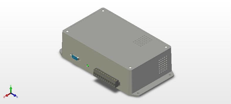
HE7VACR
May 21, 2006VERIGUARRD ACCESS CONTROL READER
Equipment Class
DXX - Part 15 Low Power Communication Device Transmitter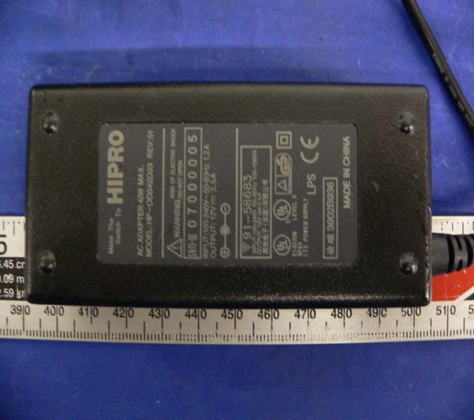
HE7PCR
Apr 06, 2005Receiver
Equipment Class
CYY - Communications Receiver used w/Pt 15 Transmitter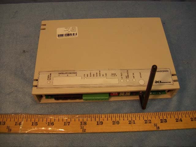
HE7EAC
Feb 07, 2005Transceiver
Equipment Class
DCD - Part 15 Low Power Transmitter Below 1705 kHz
HE7R4R
Oct 13, 2004Communications Receiver
Equipment Class
CYY - Communications Receiver used w/Pt 15 Transmitter
HE7MT2
Sep 29, 2004RFID Tag Reader
Equipment Class
DSR - Part 15 Remote Control/Security Device Transceiver