HE7PT2Patient Tag
Xmark Corporation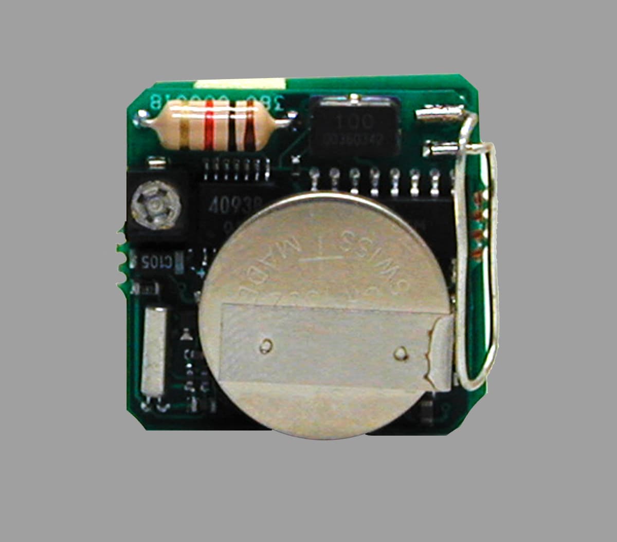
Click to zoom
Application Details
- Equipment Class
- DSC - Part 15 Security/Remote Control Transmitter
- Date of Grant
- Feb 06, 2001
- Application Purpose
- Original Equipment
- Date of Application
- Dec 14, 2000
- Equipment Note
- Patient Tag
- Frequency Range
- 433.92000000 - 433.92000000
- Company
- Xmark Corporation
- Country
- Canada
Documents & Files
Document Text
Text extracted from the exhibit documents filed with the FCC. Open a document above to read the original.
Users Manual
Revision 6.0 User Manual December 2000 March 2000, Revision 5.0, Added FCC Regulations December 2000, Revision 6.0, Added new features from HALO™ software version 3.1 © Copyright 2000, EXI Wireless Systems Inc., All rights reserved. EXI HALO User Manual980-000002-000 EXI Wireless Systems Inc.2December 2000 Revision 6.0 Table of Contents ABOUT THIS DOCUMENT..........................................................................................................................3 1.SYSTEM INTRODUCTION..................................................................................................................5 1.1.S YSTEM C OMPONENTS ......................................................................................................................5 1.2.T ERMS USED IN THIS DO CUMEN T ........................................................................................................5 1.3.C O MPUTER D ISPLAY C ONVENTIONS ..................................................................................................6 2.USER LEVEL FUNCTIONS..................................................................................................................8 2.1.A DMITTING A P ATIENT .......................................................................................................................8 2.2.D ISCHARGING OR E DITING A P ATIENT ..............................................................................................11 2.3.D ISABLING A T AG T EMPORARILY .....................................................................................................13 2.4.S ILENCING AND A CCEPTING A LARMS ..............................................................................................15 2.5.“N URSE S AVER ” AND “L O ITERIN G ” F EATURES .................................................................................17 2.6.I MPROPERLY S TO RED T AGS ..............................................................................................................17 3.SUPERVISOR LEVEL FUNCTIONS.................................................................................................19 3.1.A CCESSING S UPERVISOR L EVEL .......................................................................................................19 3.2.E XITING S UPERVISOR L EVEL ............................................................................................................20 4.ACTIVITY LOG MANAGEMENT.....................................................................................................21 4.1.A CTIVITY L OGS ................................................................................................................................21 4.2.N AVIGATING THE ACTIVITY LOG .......................................................................................................22 4.3.A DDING A S UPERVISOR ANNOTATION TO AN ALARM ........................................................................22 4.4.B ACKING UP A CTIVITY L OGS ...........................................................................................................23 5.MANAGING TAGS..............................................................................................................................24 5.1.T AGS ...............................................................................................................................................24 5.2.A DDING A NEW P-T AG TO THE SYSTEM ............................................................................................25 5.3.D ELETIN G A P-T AG FRO M THE SYSTEM .............................................................................................26 5.4.D ISABLING A P-T AG .........................................................................................................................27 5.5.U NASSIGNING A P-T AG ....................................................................................................................27 5.6.E DITING A P-T AG R ECO RD ...............................................................................................................28 5.7.C HANGING A T AG ’ S E XPIRY D ATE ...................................................................................................28 5.8.L O CATE A T AG .................................................................................................................................29 6.MANAGING SYSTEM USERS...........................................................................................................30 6.1.A DDIN G A N EW USER TO THE SYSTEM ...............................................................................................31 6.2.D ELETIN G A USER FRO M THE SYSTEM ...............................................................................................32 6.3.D ISABLIN G A SYSTEM USER ..............................................................................................................32 6.4.E DITIN G A SYSTEM USER ’ S ACCESS LEVEL ........................................................................................32 7.PRINTING LOGS................................................................................................................................33 8.MANAGING ALARM ANNOTATIONS............................................................................................34 8.1.A DDING AN A NNOTATION ...............................................................................................................35 8.2.D ELETIN G AN A NNOTATION .............................................................................................................35 8.3.E DITING AN A NNOTATION ...............................................................................................................35 9.SHUTTING DOWN AND RESTARTING THE SYSTEM................................................................36 9.1.S HUTTING DOWN .............................................................................…
Text truncated - open the document above for the full version.
Attestation Statements
EXI HALO User Manual980-000002-000 EXI Wireless Systems Inc.page numberdate and revision APPENDIX B – FCC REGULATIONS This device complies with Part 15 of the FCC Rules. Operation is subject to the following two conditions: (1) This device may not cause harmful interference, and (2) This device must accept any interference received, including interference that may cause undesired operation. This equipment has been tested and found to comply with the limits for Class B Digital Device, pursuant to Part 15 of the FCC Rules. These limits are designed to provide reasonable protection against harmful interference in a residential installation. This equipment generates and can radiate radio frequency energy and, if not installed and used in accordance with the instructions, may cause harmful interference to radio communications. However, there is no guarantee that interference will not occur in a particular installation. If this equipment does cause harmful interference to radio or television reception, which can be determined by turning the equipment off and on, the user is encouraged to try to correct the interference by one or more of the following measures. • Reorient or relocate the receiving antenna • Increase the separation between the equipment and receiver • Connect the equipment into an outlet on a circuit different from that to which the receiver is connected • Consult the dealer or an experienced radio/TV technician for help Any changes or modifications not expressly approved by the party responsible for compliance could void the user’s authority to operate the equipment. EXI Wireless SystemsModel No.: Patient Tag CANADA: 287710217261AFCC ID: HE7 PTG * This device complies with Part 15 of the FCC Rules. Operation is subject to the following two rules: (1) This device may not cause harmful interference, and (2) This device must accept any interference received, including interference that may cause undesired operation. Made in Canada EXI Wireless SystemsModel No.: Patient Tag CANADA: TBDFCC ID: HE7 PT2 * This device complies with Part 15 of the FCC Rules. Operation is subject to the following two rules: (1) This device may not cause harmful interference, and (2) This device must accept any interference received, including interference that may cause undesired operation. Made in Canada EXI Wireless SystemsModel No.: Halo Infant/ECO tag CANADA: TBDFCC ID: HE7 ETG * This device complies with Part 15 of the FCC Rules. Operation is subject to the following two rules: (1) This device may not cause harmful interference, and (2) This device must accept any interference received, including interference that may cause undesired operation. Made in Canada EXI HALO User Manual980-000002-000 EXI Wireless Systems Inc.page numberdate and revision EXI Wireless SystemsModel No.: Halo Asset tag CANADA: TBDFCC ID: HE7 ATG * This device complies with Part 15 of the FCC Rules. Operation is subject to the following two rules: (1) This device may not cause harmful interference, and (2) This device must accept any interference received, including interference that may cause undesired operation. Made in Canada
ID Label/Location Info
FCC LABEL DOCUMENT Suite 100 13551 Commerce Parkway Richmond, BC Ca n a da V6V 2L1 Phone (604) 207-7760 1-800-667-9689 Fax (604) 207-7765 e-mail: [email protected] 0.82 1.15 BOTTOM VIEW PTAG2 NOT TO SCALE DIM IN INCHES SIDE VIEW CLEAR PLASTIC BOTTOM CASE LABEL IS MOUNTED INSIDE THE BOTTOM CASE AND IS READ FROM OUTS IDE THE CASE, LABEL CAN NOT BE REMOVED WITHOUT DESTROYING THE TAG SCANNED 1 : 1 VIEW OF LABEL FCC LABEL DOCUMENT
ID Label/Location Info
FCC LABEL DOCUMENT Actual Size of Label Suite 100 13551 Commerce Parkway Richmond, BC Ca n a da V6V 2L1 Phone (604) 207-7760 1-800-667-9689 Fax (604) 207-7765 e-mail: [email protected] 0.82 1.15 BOTTOM VIEW PTAG2 NOT TO SCALE DIM IN INCHES SIDE VIEW CLEAR PLASTIC BOTTOM CASE LABEL IS MOUNTED INSIDE THE BOTTOM CASE AND IS READ FROM OUTS IDE THE CASE, LABEL CAN NOT BE REMOVED WITHOUT DESTROYING THE TAG
Operational Description
Regulatory Technical Description2000-025970-000013-000 Rev 0.2 EXI Wireless Systems Inc.1 of 7May 02, 2000 CONFIDENTIAL REGULATORY TECHNICAL DESCRIPTION Patient TAG 2 Revision 0.2 -- 28 November 2000 Document Number: 970-000023-000 Project Number: 2000-025 Regulatory Technical Description2000-025970-000013-000 Rev 0.2 EXI Wireless Systems Inc.2 of 7May 02, 2000 CONFIDENTIAL REVISIONDATECHANGED BYDESCRIPTION 0.108/11/00B. BARLOWORIGINAL 0.228/11/00B. BarlowCorrected Figure titles, Add Note p.7 Add RBC note p. 6 Regulatory Technical Description2000-025970-000013-000 Rev 0.2 EXI Wireless Systems Inc.3 of 7May 02, 2000 CONFIDENTIAL 1 PURPOSE This document is a technical description of the Patient TAG 2 (or PTAG2) product for the expressed use in regulatory evaluation. Some details are considered proprietary and confidential; therefore, reproduction or transmission of any part or in whole and in any form without consent of EXI Wireless Systems Inc. is expressly prohibited. 2 THEORY OF OPERATION The primary function of the PTAG2 (TAG) is to identify itself to an EXI TAG monitoring system. The TAG is a battery powered active device that communicates with system controllers wirelessly. Over the air communication is full duplex using pulse width coded OOK modulation. The Controller communicates with and identifies the TAG by means of a proprietary wireless protocol. A Controller generates a local pulsed RF field at 307 kHz, and a TAG in t he field will respond at 433.92 MHz. The ‘tag in field’ (TIF) identification is accomplished in a full duplex burst of code. The patented bit-by-bit protocol is inherently anti collision. After identification, the tag will not respond to the low frequency field for at least 11 seconds. The Patient TAG 2 uses a patented body sensor to detect an off body event and transmits its ID in a single burst of Pulse Width coded OOK modulation at 433.92 MHz. The TAG is designed to meet the limits of FCC Part 15.231(e) for unlicensed operation. 2.1 307 kHz RECEIVER The receiver is single conversion with a Local Oscillator at 304 kHz, ± 1 kHz. The IF Bandwidth is nominally 2 kHz. The 307 kHz receive antenna is internal to the sealed plastic case. 2.2 433.92 MHz TRANSMITTER The transmitter is a single stage, on-off keyed oscillator, stabilized by a SAW resonator. An integral wire loop antenna is the load for the oscillator and is inaccessible to the user. Frequency stability is ± 75 kHz. 2.3 PROCESSOR and I/0 An 8-bit microprocessor, running at 20.75 kHz from a fundamental 83 kHz crystal oscillator, pulse modulates the 433.92 MHz transmit signal and decodes the received baseband 307 kHz data stream. The processor is normally powered down and is energized when a ‘Wake-up’ signal is decoded by hardwired logic, or when an ‘off body’ sensor flag is detected. The processor, therefore runs only during communication with the RFID system. Regulatory Technical Description2000-025970-000013-000 Rev 0.2 EXI Wireless Systems Inc.4 of 7May 02, 2000 CONFIDENTIAL 3 DATA WAVEFORMS 3.1 TAG IN FIELD (TIF) Communication Signals The upper trace (2) in Figure 3.1 is the decoded 433.92 MHz signal transmitted by the TAG in response to the ‘Wake-up and Respond’ signal transmitted by a Controller at 307 kHz, lower trace (1) of Figure 3.1. This generates the maximum communication duty cycle for the 433.92 MHz signal in this mode. The maximum duty cycle over a 100 msec period is 0.1125. This is based on a maximum peak power transmission of 25 pulses of 350 usec and 5 pulses of 500 usec during a 100 msec period. The maximum 433.92 MHz signal burst duration in TIF mode is 85 msec. The TAG will not repeat this process unless in the field for more than 60 seconds. FIG 3.1Upper Trace (2): Decoded 433.92 MHz Tag ID Response Data Stream Lower Trace (1): TX Wake UP, Respond & Interrogate Data Stream Regulatory Technical Description2000-025970-000013-000 Rev 0.2 EXI Wireless Systems Inc.5 of 7May 02, 2000 CONFIDENTIAL 3.2 TAG Initiated Communication (TIC) Signal When the processor is awakened and detects an off body signal, it initiates a one-way communication (TIC message) to the system Controllers and Receivers. This is a single burst of code from which the system determines the ID of the TAG and ‘off-body’ alarm condition. Figure 3.2 is the baseband decoded 433.92 MHz signal transmitted by the TAG. This is pulse-width encoded OOK modulation. The maximum duty cycle occurs for an AA AA AA AA hex code sequence repeated three times. The pattern transmitted will be unique to each TAG in that it is constituted of 3 bytes of unique ID and one byte of checksum. In each case the duty cycle will be less than the maximum pattern, therefore the use of the maximum duty cycle for peak to average power adjustment includes a factor of safety. The maximum signal duration (FF FF FF FF) sequence would be 65 msec. The maximum duty cycle over a 100 msec sample time would be 0.27 based on the AA AA AA AA code. Note that each Byte is appended with a 250 usec stop bit. The message is repeated at intervals of 11 seconds minimum, doubling to a nominal message repetition interval of 2 minutes. The ‘Off body’ alarm is defeated by placing the TAG on the patient or within its conductive storage package. FIG 3.2Decoded 433.92 MHz Off Body Message Regulatory Technical Description2000-025970-000013-000 Rev 0.2 EXI Wireless Systems Inc.6 of 7May 02, 2000 CONFIDENTIAL 4 TESTING PTAG2 WITH R3 CONTROLLER The EXI series of controllers are used in development and manufacturing performance verification testing. The current version is R2, EXI PN 600-000080-000. Figure 4.1: Test Setup for Evaluation with R2 controller The TAG is excited by the 307 kHz field it will respond at 433.92 MHz in the bit-by-bit ID protocol. In the normal system operating mode, the tag would respond only once ever 60 seconds. A TEST mode is available in the Controller which forces the TAG to complete the response on every ‘Wake-up and Respond’ interrogation from the Controll…
Text truncated - open the document above for the full version.
Parts List/Tune Up Info
Multilevel Bill of MaterialsEXI #: 600-000101-000 Rev: R1.00 PTAG2 Top Level Assembly Lvl Item EXI Part # Description Rev Qty Reference Designators/Notes Vendor Name Vendor Part Number 1 1 400-000030-001 Top Case, PTAG2, EXI, Blue R1.00 1 TOP CASE Hong Kong Mould Manufacturing 400-000030-001 1 2 500-000001-000 Foil Bag for Storage of Tags R1.00 1 FOIL BAG Induspac MIL-B-131H Class I 1 3 510-000001-000 Bar Code Label for Tags R1.00 1 BAR CODE 1 4 510-000002-000 Information Label for Tags R1.00 1 INFO LABEL 1 5 530-000002-000 Methyl Ethyl Ketone (MEK) Bonding Agent R1.00 1 MEK 1 6 600-000090-000 PTAG2 PCA with Battery, Antenna, Bottom Case R1.00 1 PCA1 2 1 303-000000-000 Battery, Li-Mn, 1632, 125mA, 3V, 2-pin Horiz. Mnt. R1.00 1 BT1 Renata CR1632FH 2 2 400-000025-000 PTAG2 Wire Antenna R0.10 1 L2 2 3 400-000031-001 Bottom Case, PTAG2, Clear R1.00 1 BOTTOM CASE Hong Kong Mould Manufacturing 400-000031-001 2 4 510-000018-000 Label, PTAG2, Serial Number and Expiry Date R1.00 1 LBL1 FASTSIGNS 510-000018-000 2 5 530-000005-000 Double-sided Adhesive, Die Cut, PTAG2 R0.10 1 ADHESIVE Sytek 530-000005-000 2 6 530-000006-000 Adhesive Foam Separator, PTAG2 R0.10 1 FOAM 2 7 600-000091-000 PTAG2 PCA without Battery R1.00 1 PCA1 3 1 100-000002-2004 RES, 2.00M, SMD, 1%, 1/16W, 0402, -55 to +125C R1.00 1 R13 Rohm MCR01F2004MZS Venkel CR0402-16W-2004FT 3 2 100-000002-3573 RES, 357K, SMD, 1%, 1/16W, 0402, -55 to +125C R1.00 1 R50 Cal-Chip RM04F3573CT KOA RK73H1ETP3573F Panasonic ERJ2RKF3573X Rohm MCR01F3573MZS Samsung RC1005F3573CS Venkel CR0402-16W-3573FT Vishay CRCW04023573FRT5 3 3 100-000002-4753 RES, 475K, SMD, 1%, 1/16W, 0402, -55 to +125C R1.00 1 R49 Cal-Chip RM04F4753CT KOA RK73H1ETP4753F Panasonic ERJ2RKF4753X Rohm MCR01F4753MZS Samsung RC1005F4753CS Venkel CR0402-16W-4753FT Vishay CRCW04024753FRT5 3 4 100-000003-000 RES, 0, SMD, 5%, 1/16W, 0402, -55 to +125C R1.00 2 R15, R54 AVX CR05-000-H Cal-Chip RM04J0000CT KOA RM73Z1ET000 Panasonic ERJ2GEOR00X Rohm MCR01J000MZS Samsung RC1005J000CS Venkel CR0402-16W-000JT Vishay CRCW0402000RT5 3 5 100-000003-103 RES, 10K, SMD, 5%, 1/16W, 0402, -55 to +125C R1.00 2 R1, R2 AVX CR05-103J-H Cal-Chip RM04J103CT KOA RM73B1ET103J Panasonic ERJ2GEJ103X Rohm MCR01J103MZS Samsung RC1005J103CS Venkel CR0402-16W-103JT Vishay CRCW0402103JRT5 3 6 100-000003-104 RES, 100K, SMD, 5%, 1/16W, 0402, -55 to +125C R1.00 2 R21, R38 AVX CR05-104J-H Cal-Chip RM04J104CT KOA RM73B1ET104J Panasonic ERJ2GEJ104X Rohm MCR01J104MZS Samsung RC1005J104CS Venkel CR0402-16W-104JT Vishay CRCW0402104JRT5 3 7 100-000003-105 RES, 1M, SMD, 5%, 1/16W, 0402, -55 to +125C R1.00 3 R39, R41, R48 AVX CR05-105J-H Cal-Chip RM04J105CT KOA RM73B1ET105J Panasonic ERJ2GEJ105X Rohm MCR01J105MZS Samsung RC1005J105CS Venkel CR0402-16W-105JT Vishay CRCW0402105JRT5 3 8 100-000003-134 RES, 130K, SMD, 5%, 1/16W, 0402, -55 to +125C R1.00 1 R33 AVX CR05-134J-H Cal-Chip RM04J134CT KOA RM73B1ET134J Panasonic ERJ2GEJ134X Rohm MCR01J134MZS Samsung RC1005J134CS Venkel CR0402-16W-134JT Vishay CRCW0402134JRT5 3 9 100-000003-155 RES, 1.5M, SMD, 5%, 1/16W, 0402, -55 to +125C R1.00 1 R37 AVX CR05-155J-H Cal-Chip RM04J155CT KOA RM73B1ET155J Panasonic ERJ2GEJ155X Rohm MCR01J155MZS Samsung RC1005J155CS Venkel CR0402-16W-155JT 3 10 100-000003-183 RES, 18K, SMD, 5%, 1/16W, 0402, -55 to +125C R1.00 1 R52 AVX CR05-183J-H Cal-Chip RM04J183CT KOA RM73B1ET183J Panasonic ERJ2GEJ183X Rohm MCR01J183MZS Samsung RC1005J183CS Venkel CR0402-16W-183JT Vishay CRCW0402183JRT5 3 11 100-000003-225 RES, 2.2M, SMD, 5%, 1/16W, 0402, -55 to +125C R1.00 6 R7, R16, R17, R20, R27, R44 AVX CR05-225J-H Cal-Chip RM04J225CT KOA RM73B1ET225J Panasonic ERJ2GEJ225X Rohm MCR01J225MZS Samsung RC1005J225CS Venkel CR0402-16W-225JT 3 12 100-000003-274 RES, 270K, SMD, 5%, 1/16W, 0402, -55 to +125C R1.00 1 R36 AVX CR05-274J-H Cal-Chip RM04J274CT KOA RM73B1ET274J Panasonic ERJ2GEJ274X Rohm MCR01J274MZS Samsung RC1005J274CS Venkel CR0402-16W-274JT Vishay CRCW0402274JRT5 3 13 100-000003-275 RES, 2.7M, SMD, 5%, 1/16W, 0402, -55 to +125C R1.00 1 R51 Cal-Chip RM04J275CT KOA RM73B1ET275J Rohm MCR01J275MZS Venkel CR0402-16W-275JT 3 14 100-000003-333 RES, 33K, SMD, 5%, 1/16W, 0402, -55 to +125C R1.00 1 R53 AVX CR05-333J-H Cal-Chip RM04J333CT KOA RM73B1ET333J Panasonic ERJ2GEJ333X Rohm MCR01J333MZS Samsung RC1005J333CS Venkel CR0402-16W-333JT Vishay CRCW0402333JRT5 3 15 100-000003-474 RES, 470K, SMD, 5%, 1/16W, 0402, -55 to +125C R1.00 1 R24 AVX CR05-474J-H Cal-Chip RM04J474CT KOA RM73B1ET474J Panasonic ERJ2GEJ474X Rohm MCR01J474MZS Samsung RC1005J474CS Venkel CR0402-16W-474JT Vishay CRCW0402474JRT5 3 16 100-000003-821 RES, 820, SMD, 5%, 1/16W, 0402, -55 to +125C R1.00 1 R22 AVX CR05-821J-H Cal-Chip RM04J821CT KOA RM73B1ET821J Panasonic ERJ2GEJ821X Rohm MCR01J821MZS Samsung RC1005J821CS Venkel CR0402-16W-821JT Vishay CRCW0402821JRT5 3 17 100-000006-4754 RES, 4.75M, SMD, 1%, 1/16W, 0603, -55 to +125C R1.00 2 R18, R26 KOA RK73H1J4754F Philips 9C06031A4754FKRFT 3 18 100-000008-106 RES, 10M, SMD, 5%, 1/16W, 0603, -55 to +125C R1.00 15 R3, R4, R5, R6, R8, R9, R10, R11, R12, R19, R23, R25, R29, R31, R32 AVX CR10-106J-T Bourns CR0603-JW-106E Chip Technologies Inc. CR0603J106T1 KOA RM73B1JT106J Panasonic ERJ3GSYJ106V Rohm MCR03J106EZH Venkel CR0603-16W-106JT 3 19 100-000008-475 RES, 4.7M, SMD, 5%, 1/16W, 0603, -55 to +125C R1.00 1 R35 AVX CR10-475J-T Bourns CR0603-JW-475E Cal-Chip RM06J475CT Chip Technologies Inc. CR0603J475T1 KOA RM73B1JT475J Panasonic ERJ3GSYJ475V Rohm MCR03J475EZH Venkel CR0603-16W-475JT 3 20 100-000008-685 RES, 6.8M, SMD, 5%, 1/16W, 0603, -55 to +125C R1.00 2 R30, R40 AVX CR10-685J-T Bourns CR0603-JW-685E Chip Technologies Inc. CR0603J685T1 KOA RM73B1JT685J Panasonic ERJ3GSYJ685V Rohm MCR03J685EZH Venkel CR0603-16W-685JT 3 21 100-000008-825 RES, 8.2M, SMD, 5%, 1/16W, 0603, -55 to +125C R1.00 2 R46, R47 AVX CR10-825J-T Bourns CR0603-JW-825E Chip Technologies Inc. CR0603J825T1 KOA RM73B1JT825J Panasonic ERJ3GSYJ825V Rohm MCR03J825EZH Venkel CR0603-16W-825JT 3 22 110-000001…
Text truncated - open the document above for the full version.
Schematics
5 5 4 4 3 3 2 2 1 1 DD CC BB AA '1' - Battery good '0' - Battery weak Battery Monitor From Sensor Board To Receiver section Wake-up (from Sensor board) R52 changed to decrease hysteresis. RXD will stay High until uC loses power - RX can miss next Wake-up word if C18 is large enough. C18 charges to a much higher voltage when uC maintains power line than when the counter causes tag to power up (due to instant Reset pulse in the latter case). The difference is worse for small-hysteresis gates, such as Rohm's. Flex Strip Connector to Sensor Board Do not place R28 0.20B 24Friday, September 22, 2000 Ptag2-Digital Circuit 911-000007-000 EXI Wireless Systems Confidential Title SizeDocument NumberRev Date:Sheetof Rx_MP Hold_Pwr Gnd Vcc Rx Tx RXD Gnd Vcc R23 10Meg R24 470K R26 4.75Meg 1%U7B MBT3946DW1T1 6 2 1 U9 12C509-04/SM 1 2 3 7 6 5 4 8 VDD OSC1 OSC2 GP0 GP1 GP2 GP3 GND U7A MBT3946DW1T1 3 5 4 C20 1uF Tantalum C19 820p R27 2.2Meg C18 27n X7R C23 10p C21 10p C22 33p U6D BU4093BFV 13 12 7 14 11 U15 LTC1540 12 3 4 5 6 8 7 GNDREF- + - HYST REF+ OUT VCC R49 475K 1% U8 CD4017BCM 14 13 15 3 2 4 7 10 1 5 6 9 11 12 16 8 CLK ENA RST Q0 Q1 Q2 Q3 Q4 Q5 Q6 Q7 Q8 Q9 CO VDD VSS R50 357K 1% R28 470k U6A BU4093BFV 1 2 3 Q5 MMBT2484LT1 3 1 2 U6C BU4093BFV 8 9 10 U5A MBT3906DW1T1 3 5 4 U6B BU4093BFV 5 6 4 U5B MBT3906DW1T1 6 2 1 R51 2.7MEG R29 10Meg R44 2.2MEG R52 18K R48 1MEG Y2 C-2 83.000KC-P R30 6.8Meg R25 10Meg Main-NPWR_ON Main-RD Main-Vcc Gnd
Schematics
5 5 4 4 3 3 2 2 1 1 DD CC BB AA Antenna connections should be accomplished on the bottom side of the PCB, retaining existing trace geometry. Antenna pads should exist on both sides of the board and utilize two vias each for mechanical strength. The pads must be open, i.e. without solder mask. Tx Section Wire Antenna 400-000025-000 0.20B 34Friday, September 22, 2000 Ptag2 - RF 911-000021-000 EXI Wireless Systems Confidential Title SizeDocument NumberRev Date:Sheetof Rx_PWR2 Gnd Rx_PWR1Vcc Rx RXD Tx Vcc Gnd C17 100n X7R C7 100p R21 100K R22 820 ohm R19 10Meg C1 100n X7R C4 47p BT1 CR1632 FH 1 23 C14 56p U4A MBT3946DW1T1 3 5 4 L1 1mH R18 4.75Meg 1% C8 27p R9 10Meg C138.2p L227.5nH R4 10Meg C11 2.2nR33 130K R11 10Meg U1B MBT3904DW1T1 6 2 1 C24 47p R6 10Meg R12 10Meg Q1 MMBT2484LT1 3 1 2 Q4 MMBTH10LT1 3 1 2 R13 2.0Meg 1%R17 2.2Meg R8 10Meg C3 2.2n R16 2.2Meg R15 0 ohm R10 10Meg R7 2.2Meg C5 47p R3 10Meg Q2 MMBT5087LT1 3 1 2 R20 2.2Meg R5 10Meg Q3 MMBT2484LT1 3 1 2 U3B MBT3904DW1T1 6 2 1 C6 470p U3A MBT3904DW1T1 3 5 4 U4B MBT3946DW1T1 6 2 1 C9 7-50p C16 10p C10 470p U2A MBT3946DW1T1 3 5 4 U1A MBT3904DW1T1 3 5 4 R1 10k R2 10k C12 220p C2 100n X7R Y1 RO2101A - 433.92MHz R32 10Meg C15 2.7p U2B MBT3946DW1T1 6 2 1 R31 10Meg
Schematics
5 5 4 4 3 3 2 2 1 1 DD CC BB AA Note: Shielding is required between the RF and digital sections to ensure that high frequency components of the digital signals are not coupled into the receiver. A ground plane between the two circuits (layers) should be sufficient to provide this shielding. Design Notes: Revision Status: R 0.10 - first prototype spin Component Notes: (These notes will appear in the BOM) TX layout should be retained unchanged from previous release with the following exception: antenna pads should exist on both sides of the PCB and use two vias each for inter-layer connections. Connections to the pads should be accomplished on the bottom layer since the rest of the parts are located there. Traces from the top side should be removed. Tx Section R 0.20 - second prototype spin 0.20 B 14Friday, September 22, 2000 Ptag2 911-000021-000 ConfidentialEXI Wireless Systems Title SizeDocument NumberRev Date:Sheetof Main Main-RD Main-Vcc Gnd Main-NPWR_ON Sensor Sensor-Vcc Gnd Sensor-NPWR_ON Sensor-RD GNDGND A1 All capacitors are type NPO unless otherwise noted A2 All resistors, capacitors, and inductors have 5% tolerances unless otherwise noted J3 300-000029-004 1 2 3 45 6 7 8 A3 All capacitor voltages are 16v or greater unless otherwise noted
Schematics
5 5 4 4 3 3 2 2 1 1 DD CC BB AA Operating frequency 7HzR36 - Sensitivity adjustment Greater value requires firmer skin contact ESD protection Solder bridge (Weaker skin contact) Flex Jumper to Main Board 911-000021-0000.20 Ptag2 - Body Sensor B 44Friday, September 22, 2000 EXI Wireless Systems Confidential Title SizeDocument NumberRev Date:Sheetof Vcc Vcc Vcc Vcc Vcc R35 4.7MEG R39 1MEG U13B MC14001BDT 5 6 4 U12 LTC1540CMS8 12 3 4 5 6 8 7 GNDREF- + - HYST REF+ OUT VCC C26 33pF R36 270K 0.8 0.3 8 C27 CS038x08 1 1 R37 1.5MEG U13C MC14001BDT 8 9 10 C29 100n R40 6.8MEG R38 100K U14B MBT3946DW1T1 6 2 1 U14A MBT3946DW1T1 3 5 4 R46 8.2MEGU13A MC14001BDT 2 1 3 14 7 C25 10n R47 8.2MEG R53 33K R54 0 C30 100n R41 1MEG U13D MC14001BDT 12 13 11 C28 1n Sensor-Vcc Sensor-RD Sensor-NPWR_ON Gnd
Test Report
Master: ktlPT15231 Date: April 5, 2000 KTL Test Report:0R03227 Applicant:EXI Wireless Systems Inc. Suite 100 – 13551 Commerce Pk. Richmond, BC V6V 2L1 Equipment Under Test:Patient Tag 2 (E.U.T.) FCC ID:HE7PT2 In Accordance With:FCC Part 15, Subpart C For Low Power Transmitters Operating Periodically In The Band 40.66 - 40.77 MHz And Above 70 MHz Tested By:KTL Ottawa Inc. 3325 River Road, R.R. 5 Ottawa, Ontario K1V 1H2 Authorized By: G. Westwell, Technologist Date: Total Number of Pages:14 KTL Ottawa FCC PART 15, SUBPART C FOR LOW POWER TRANSMITTERS PROJECT NO.: 0R03227 EQUIPMENT: Patient Tag 2 FCC ID: HE7PT2 Page 2 of 14 Table of Contents Section 1. Summary of Test Results.......................................................................................... 3 Section 2. Equipment Under Test (E.U.T.) .............................................................................. 5 Section 3. Occupied Bandwidth................................................................................................ 9 Section 4. Periodic Alternate Field Strength Requirements................................................ 11 Section 5. Block Diagrams.......................................................................................................13 Section 6. Test Equipment List ............................................................................................... 14 KTL Ottawa FCC PART 15, SUBPART C FOR LOW POWER TRANSMITTERS PROJECT NO.: 0R03227 EQUIPMENT: Patient Tag 2 FCC ID: HE7PT2 Page 3 of 14 Section 1.Summary of Test Results General All measurements are traceable to national standards. These tests were conducted on a sample of the equipment for the purpose of demonstrating compliance with Part 15, Subpart C, Paragraph 15.231. All tests were conducted using measurement procedure ANSI C63.4-1992. Radiated emissions are made on an open area test site. A description of the test facility is on file with the FCC. New SubmissionProduction Unit Class II Permissive ChangePre-Production Unit DS C Equipment Code THIS TEST REPORT RELATES ONLY TO THE ITEM(S) TESTED. THE FOLLOWING DEVIATIONS FROM, ADDITIONS TO, OR EXCLUSIONS FROM THE TEST SPECIFICATIONS HAVE BEEN MADE. See “ Summary of Test Data”. NVLAP LAB CODE: 100351-0 TESTED BY: _____________________________________ DATE: ___________________ Russell Grant, Wireless Group Manager KTL Ottawa Inc. authorizes the above named company to reproduce this report provided it is reproduced in its entirety and for use by the company’s employees only. Any use which a third party makes of this report, or any reliance on or decisions to be made based on it, are the responsibility of such third parties. KTL Ottawa Inc. accepts no responsibility for damages, if any, suffered by any third party as a result of decisions made or actions based on this report. This report applies only to the items tested. KTL Ottawa FCC PART 15, SUBPART C FOR LOW POWER TRANSMITTERS PROJECT NO.: 0R03227 EQUIPMENT: Patient Tag 2 FCC ID: HE7PT2 Page 4 of 14 Summary Of Test Data Name of TestPara. NumberResults Transmission Requirements15.231(a)Not Applicable Radiated Emissions15.231(b)Not Applicable Occupied Bandwidth15.231(c)Complies Frequency Tolerance15.231(d)Not Applicable Periodic Alternate Field Strength Requirements15.231(e)…
Text truncated - open the document above for the full version.
Contact Information
Applicant
Chris Bisaillion(Senior RF Designer)
Technical Contact
Non-Technical Contact
KTL OTTAWA INC.RUBY C DULMAGE
[email protected]613-737-9680
Test Firm
Nemko Canada Inc.Stuart Beck
Technical Specifications
| # | Rule Parts | Frequency Range | Power Output |
|---|---|---|---|
| 1 | 15C | 433.92 MHz - 433.92 MHz | - |
Other Applications from Xmark Corporation
HE7VH2R
Oct 18, 2006VERICHIP H2 READER
Equipment Class
DXX - Part 15 Low Power Communication Device Transmitter
HE7VACR
May 21, 2006VERIGUARRD ACCESS CONTROL READER
Equipment Class
DXX - Part 15 Low Power Communication Device Transmitter
HE7PCR
Apr 06, 2005Receiver
Equipment Class
CYY - Communications Receiver used w/Pt 15 Transmitter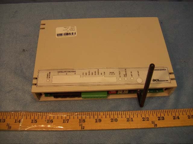
HE7EAC
Feb 07, 2005Transceiver
Equipment Class
DCD - Part 15 Low Power Transmitter Below 1705 kHz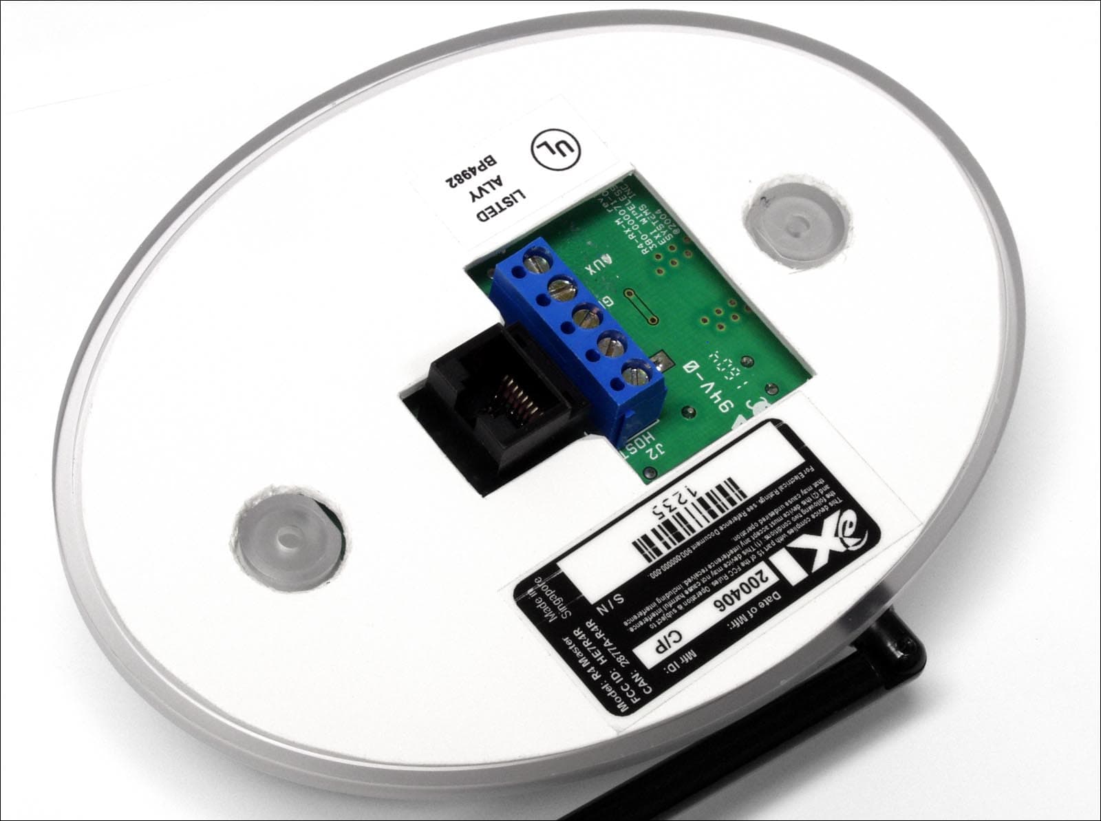
HE7R4R
Oct 13, 2004Communications Receiver
Equipment Class
CYY - Communications Receiver used w/Pt 15 Transmitter