OOX-LMS3000Wireless LAN Node
Vecima Networks Inc.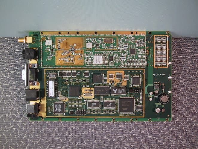
Click to zoom
Application Details
- Equipment Class
- DSS - Part 15 Spread Spectrum Transmitter
- Date of Grant
- Mar 04, 2001
- Application Purpose
- Original Equipment
- Date of Application
- Mar 04, 2001
- Equipment Note
- Wireless LAN Node
- Frequency Range
- 905.00000000 - 925.00000000
- Company
- Vecima Networks Inc.
- Country
- Canada
Documents & Files
Document Text
Text extracted from the exhibit documents filed with the FCC. Open a document above to read the original.
Users Manual
Warranty In the following warranty text, “WaveRider®” shall mean WaveRider CommunicationsInc. This WaveRider product is warranted against defects in material and workmanship for a period of one (1) year from the date of purchase. During this warranty per iod WaveRider will, at its option, either repair or replace products that pro ve to be defecti ve. For warranty service or repair, the product must be returned to a service facility designated by WaveRider. Authoriz ati on to return products must be obt ained prior to sh ipment. The WaveRider RMA number must be on the shipping documenta tion so that the service fac ility will accept the product. The buyer shall pay all shi pping charges to WaveRider and WaveRider shall pay shi pping charges to return the product to t he buyer within Canada or t he USA. For all other countries, the buyer shall pay shipping charg es as well as duties and taxes incurred in shipping pro ducts to or from WaveRider. WaveRider warrants that the firmware designed by it for use with the uni t will execute its pro gramming instructions when properly i nstalled on the unit. WaveRider does not warrant that the operation of the unit or firmware will be uni nterrupted or error-free. Limitation of Warranty The foregoing warranty shall not apply to def ects resulting from impro per or inadequate maintenance by the buy er, buyer-s upplied int erfacing, unauthorized modif ication or misuse, operati on outside the environment al specifications for the product, or improper site preparation or maint enance. No other warranty is expressed or implied. WaveRider specifi cally disclaims the implied warrantie s of merchantability and fitness for any particular purpose. No Liability for Consequential Damages To the maximum extent permit ted by applicable law, in no event shall Wav eRider or its suppliers be liable for any damages whats oever (including, without limitation, damages for loss of business profits, busin ess interrupti on, loss of busin ess information, or any other pecuniary loss) ari sing from the use of or inability to use the product, eve n if WaveRider has been advised of t he possi bility of such damages, or for any claim by any other party. Because some state s/juri sdictions do not allow the exc lu sion or limitation of lia bility for consequential or incid ental damages, the above limitation may not apply to you. In no event will WaveRider’s liability exceed the amount paid for the product. Regulatory Notices This equipment h as been tested and found to comply with the limits for a Class B Intentional Radia tor, pursuant to Part 15 of the FCC Regul ations and RCC-210 of the IC Regulations. These limits are int ended to provide protect ion against harmful interference when the equipment is operate d in a residential e nvironment. This equipment generates, uses, and can radiate radio frequency energy and, if not insta lled and used in accordance with the instructi on manual, may cause harmful int erference t o radio communications . However, there is no guarant ee that int erference will not occur in a particular i nstallat ion. Notice to User Any changes or modif icatio ns to equipment that are not expre ssly approve d by the manuf acturer may void the user’s authority to operate the equipment. If an RS-232 cable is required, a shielded version is to be used to avoid interference.
Block Diagram
1. Block Diagram 1.1 Top Level Block Diagram Cavity Filter Optional CCU Only Antenna Switch Digital/Baseband Section RF Section 7.5V DC ETHERNET USB RS232 3LEDS Antenna 902- 928M Hz RF Figure 1.1 – TOP Level Block Diagram 1.2 RF Section +7.5V DC 5V LO 3.3V 5V Regulator 3.3V Regulator SYN TO RF LO 22MHzREF’ Connector Front-end Filter Coupler & Detector PATX RF Image Filter TXRF Driver TX Mixer RX Mixer RX RF Image Filter RF LNA PAPE TXRFAGC RFLEVEL RF LO 975-995MHz RX IF Filter1 ANTSEL RFSW RXRFAGC TXRX Switch IF Driver IF Amp RXIF- RXIF+ TXIF- TXIF+ XFER 7.5V PA 902-928MHz70MHz 70MHz 902-928MHz SHIELD RXIFAGC VREF TXIFAGC RXQ+/- RXI+/- TXI+/- I/Q MOD/ DEMODULATOR 140MHz IFLO IFDET TXQ+/- LEIF 22MHz REF Buffer SDATA’ SCLK’ RX IF Filter2 SHIELD SHIELD PROVISION FOR SHIELD PROVISION FOR SHIELD PROVISION FOR SHIELD PROVISION FOR SHIELD -3V Regulator -3V PA 22MHzREF’ TX IF Filter TX IF Amp TO Antenna XFER Voltage translator 7.5V Supply SDATA’ LERF SDATA SCLK EN RF AND GATES SCLK’ Figure 1.2 – RF Section Block Diagram 1.3 Digital Section MICRO PROCESSOR RS232 TRANSLATOR ETHERNET MAC/PHY MEMORY (FLASH, SDRAM) DSSS BBP LEDS DC/DC CONVERTER MAC MEMORY (FLASH, SRAM) JTAG JTAG 32.768kHz 44MHz REF OSC 3.6864MHz ÷ 2 ÷ 4 22MHzREF RXQ +/- RXI +/- TXIFAGC RXIFAGC VREF SHIELDS (TOP/BOTTOM) 7.5V 1.55V 3.3V 5.0V RESET Linear Regulator Linear Regulator SDATA SCLK LERF TXRFAGC ANTSEL RFLEVEL IFDET RXRFAGC TXI +/- TXQ +/- RFSW PAPE LEIF 15 57332 3 2 4 9 9 5 27 USB D+ TXD RXD DCD VCC GND D- DTR SG DSR RTS CTS RI ODATA- ODATA+ IDATA- IDATA+ 7 21 2 2 2 2 3.3V 2 GPIO DEBUG HEADER 2 LEDs To RF Section IN/OUTPUT Power Level : 3.3V 2 EN-RF 1.3 DIGITAL SECTION BLOCK DIAGRAM 1.3.1 Ethernet MAC/ PHY to Microprocessor Interface 44 ETHERNET MAC / PHY BLOCK – PCMCIA SOCKET 0 SMSC LAN91C96 ADDR[3..0] /IRQ /WAIT /IOIS16 RESET /CE1 DATA [15..0] GROUND IOS{2..0] 20MHz (25 PPM) RX LINK 2 IDATA- ODATA+ ODATA- IDATA+ /CE2 /IOW /IOR /W E /OE /PREG /INPACK 2 /EN16ENEEP TX LED LED 1.3.1 ETHERNET MAC / PHY To MICROPROCESSOR INTERFACE BLOCK DIAGRAM 1.3.2 Processor Memory to Microprocessor Interface GROUND DATA[31..0] PROCESSOR MEMORY BLOCK ADDR [24..0] D[15..0] A[24..0] VCC /C S0 /OE /W R A [20..10] A21 A22 MT48LC 2M32B2 SD RAM RC28F128J 3A-150 FLASH / BYTE D[15..0] A[24..1] A0 VPEN STS /R P D[31..0] A[10..0] BA0 BA1 /D QM [3..0] TO G PIO RESET DATA[31..0] D[15...0] GROUND /CAS /RAS /CS /WE /CKE /CLK 1.3.2 PROCESSOR MEMORY To MICROPROCESSOR INTERFACE BLOCK DIAGRAM 1.3.3 MAC Interface 3 PAPE, RFSW TO PROCESSOR 22 MHZ TO DEBUG HEADER CLOCKTEST[2..0 ] 3 /WAIT /IREQ DATA[15..0] ADDR[15..0] 5 MAC JTAG 5 X 2 HEADER AT76502 SDATA, SCLK LERF LEIF 14 MD_RDY, CCA, TX_PE, RX_PE, BB_R/W, /CSB, RESET_BB_n, RX_DATA, RX_CLK, S_DATA, S_CLK, TX_RDY, TX_DATA, TX_CLK SEL1 SCLK, SDATA SEL0 A[16..0]/OE /WE D[7..0] /OE/WE A[16..0 ] D[7..0] CY7C1019V33 (SRAM) AT49LV010 (FLASH) / OE/WE A[16..0] D[7..0] MAC MEMORY MAC BLOCK - PCMCIA SOCKET 1 TO RF TO BBP /IOIS16 RESET /CE1 /CE2 /IOW /IOR /WE /OE /PREG /INPACK CAL_EN, PE1, PE2 EN_RF Vcc 1.3.3 MAC INTERFACE BLOCK DIAGRAM
Cover Letter(s)
letter of confidentiality 3000 (2552x3300x2 gif)
Operational Description
LMS-3000 Functional Overview The LMS-3000 radio module is a single PCB wireless solution based on the Intersil PRISM II Direct Sequence Chip Set. The two block diagrams, one representing the RF functionality , the other the Digital functionality of the radio module are located in Figure 1 and 2. The digital section contains the following functionality: 1) I/O 2) Microprocessor 3) MAC 4) Memory 5) Reference Oscillator 6) Power Regulation The radio modules RF section contains the following functionality: 1. Baseband Processor 2. Modulator/Demodulator 3. Dual Synthesizer 4. Up/Down Converter 5. Power Amplifier 6. Low Noise Amplifier (LNA) 7. RF VCO 8. IF VCO 9. Antenna (RF) Interface During transmission , data obtained by the Microprocessor from the I/O ports, is transferred to the MAC. The MAC reformats the data and places it on the Baseband Processor TX data line. This data is modulated according to the format selected (CCK) and then spread using a defined PN code. Two signals are generated (the In-Phase (I) and Quadrature (Q) components). The I & Q signals are sent to the Modulator/Demodulator where they are first filtered and then modulated with the IF frequency (70 MHz). The IF oscillator generates a 140 MHz signal which is divided by two inside the Modulator/Demodulator, generating a final IF signal of 70 MHz. Next, the two signals are combined into a single signal and sent to the Up/Down converter. The Up/Down converter will shift this signal to the RF frequency for the channel programmed in the synthesizer, for operation within the 902-28 MHz ISM band. In the final stage, this signal is amplified to produce +26 dBm RF power output as measured at the output of the antenna port. In the receive mode, the radio signal is amplified by the LNA, and then sent to the Up/Down converter. The Up/Down converter down-converts this signal from the 902-28 MHz range to the IF frequency, 70 MHz. The Modulator/Demodulator then converts the signal to baseband and splits the signal into its I & Q components, before sending it to the Baseband Processor. Finally, the Baseband Processor despreads and demodulates the data contained in the CCK format, and places it on the RX data line to the MAC. The MAC modifies the data, then transfers it to the Microprocessor which reformats the information and sends it out the I/O ports. The RF and IF Local Oscillator signals are generated using the synthesizer and voltage controlled oscillators. The synthesizer is programmed with the desired RF channel frequency plus the IF frequency. The baseband processor and the synthesizer are driven from a common 44 MHz oscillator to control the timing of these chips. Example (for Channel 1 operation) : RF IF LO 905 MHz + 70 MHz = 975 MHz The antenna (RF) connector is connected to a 50-ohm impedance matched transmission line (Times Microwave LMR-400 or LMR-600) to one of the following antenna types: Omni, Disc, Patch, Yagi and Dipole Reflector. The table below includes examples of each of the recommended antenna types, as well as their associated maximum antenna system gain. Antenna TypeManufacturerModel NumberMaximum Antenna System Gain OmniAstronV-91835.1 dBi DiscAstronPCNLP09V3 dBi PatchAstronASTPCG09HD8.5 dBi YagiAstron928-49.1 dBi Dipole ReflectorTil-TekTA-81110.4 dBi Table 1: Antenna Types for use with the LMS-3000 +7.5V DC 5V LO 3.3V 5V Regulator 3.3V Regulator SYN TO RF LO 22MHzREF’ Connector Front-end Filter Coupler & Detector PATX RF Image Filter TX RF Driver TX Mixer RX M ixer RX RF Im age Filter RF LNA PAPE TX RFAGC RFLEVEL RF LO 975-995MHz RX IF Filter1 ANTSEL RFSW RXRFAGC TX RX Switch IF Driver IF Am p RXIF- RXIF+ TX IF- TX IF+ XFER 7.5V PA 902-928MHz70MHz 70MHz 902-928MHz SHIELD RXIFAGC VREF TX IFA GC RXQ+ /- RXI+ /- TX I+/- I/Q MOD/ DEMODULATOR 140MHz IFLO IF DET TX Q+/- LEIF 22MHz REF Buffer SDATA’ SCLK’ RX IF Filter2 SHIELD SHIELD PROV ISION F OR S HIELD PROV ISION F OR S HIELD PROV ISION F OR S HIELD PROV ISION FOR SHIELD -3V Regulator -3V PA 22MHzREF’ TX IF Filter TX IF Amp TO Antenna XFER Voltage tr anslator 7.5V Supply SDATA’ LERF SDATA SCLK EN RF AND GATES SCLK’ Figure 1 RF Section Block MIC RO PROCESSOR RS232 TRANSLATOR ETHERNET MAC/PHY MEMORY (FLASH, SDRAM) DSSS BB P LEDS DC/DC CONVERTER MAC MEMORY (FLASH, SRAM) JTAG JTAG 32.768kHz 44MHz REF OSC 3.6864MHz ÷ 2 ÷ 4 22MHzREF RXQ +/- RXI +/- TXIFAGC RXIFAGC VREF SHIELDS (TOP/BOTTOM) 7.5V 1.55V 3.3V 5.0V RESET Linear Regulator Linear Regulator SDATA SCLK LERF TXRFAGC ANTSEL RFLEVEL IFDET RXRFAGC TXI +/- TX Q +/- RFSW PAPE LEIF 15 57332 3 2 4 9 9 5 27 USB D+ TXD RXD DCD VCC GND D- DTR SG DSR RTS CTS RI ODATA- ODATA+ IDATA- IDATA+ 7 21 2 2 2 2 3.3V 2 GPIO DEBUG HEADER 2 LEDs To RF Section IN/OUTPUT Power Level : 3.3V 2 EN-RF Figure 2 Digital Section Block
RF Exposure Info
1. Radio Frequency exposure 1.1 Regulation 15.247(b4) Systems operating under the provisions of this section shall be operated in a manner that ensures that the public is not exposed to radio frequency energy levels in excess of the Commission’s guidelines. See §1.1307(b)(1) of this Chapter. 1.2 Result According to par 1.1307b(1), the EUT does not require an environmental evaluation. 1. This equipment classification is not present within table 1 of part 1.1307 and is not listed in section 1.1307b(2). 2. The EUT categorically exempt from routine environmental evaluation per section 2.1093. Included are calculations that determine that minimum distance I from the transmitter antenna that will ensure an exposure limit at or below the guidelines given in table 1 of part 1.1310 for the general population. The formula for these calculations are taken from OET Bulletin 65, edition 97-01, August 1997; “Evaluating Compliance with FCC Guidelines for Human Exposure to Radio frequency Electromagnetic Fields”. 1.3 CALCULATIONS Per Table 1 of Section 1.1310 the limit for general population exposure at 2.4 GHz is 1.0 mW/cm 2 Per OET Bulletin 65, edition 97-01 the formula for calculating power density is: S = P*G/4πR 2 with Power = 25.6 dBm = 363 mW Gain of Antenna: System = 10.4 dBi or a numeric gain of 11 therefore Solving for R gives a minimum safe distance of 17.8 cm 1.4 CONCLUSION Page 19 of the user manual instructs the installer to maintain at least a 2 meter separation between personal and the user.
Test Report
QUESTIONS: We have completed our review and the following issues were identified: 1. Please provide data responsive to the 15.31(e) requirement for input voltage variation. 2. Please specify the label material. 3. The report specifies that testing was conducted with a shielded RS-232 cable. The users manual does not specify a shielded cable should be used when connecting to the RS-232 port. Please supply a corrected users manual. 4. The users manual RF exposure statements do not refer to the EUM. Please supply a corrected users manual. Best regards Barry C. Quinlan Certification & Telecom Manager Curtis-Straus LLC ANSWERS: Dear Barry, We have compiled a response to your e-mail dated February 19, 2001. 1 - We have revised our report and attached revision A for your review. 2- The material used for the Regulatory label is Mylar. Its adhesive is manufactured by 3M, part #467MP. 3 - We have revised two pages in the user manual and attached them for your review. Regards, Desiree
Test Report
TIL-TEK TIL-TEK Antennas www.tiltek.com(613) 258-5928Form 2000-811 Rev.2.1 Specifications subject to change without notice 0 902700-3-6-10 -15 -20 -30 dB 120 0 902700-3-6-10 -15 -20 -30 dB 60 0 902700-3-6-10 -15 -20 -30 dB 90 0 902700-3-6-10 -15 -20 -30 dB 105 0 90270 0-3-6-10 -15 -20 -30 dB T0 902700-3-6-10 -15 -20 -30 dB T5 90270 0-3-6-10 -15 -20 -30 dB T10 90270 0-3-6-10 -15 -20 -30 dB T13 90270 0-3-6-10 -15 -20 -30 dB T15 TA-811 Adjustable Sector 806 - 960 MHz The TA-811 adjustable sector is a high gain broadband dipole array enclosed in an aluminum base and has an ASA UV stabilized radome for superior performance and weatherability. Extremely low side lobes, an adjustable azimuth pattern and up to 6 degrees of mechanical downtilt make this a remarkably versatile antenna. Electrical Specifications Frequency Range: 806-866, 824-896, 872-960 MHz Gain: (dBd) 15.5 @ 60 0 14 @ 90 0 13.75 @ 105 0 13.5 @ 120 0 VSWR: 1.5:1 max. 1.35:1 typical Front/Back Ratio: 25 dB min. 30 dB typical Polarization: Vertical Power Rating: 500 Watts H-Plane Beamwidth: 60, 90, 105, 120 degrees E-Plane Beamwidth: 8.5 degrees Electrical Downtilt: 0, 5, 10, 13, 15 degrees Cross Pol. Discrimination: 20 dB min. Impedance: 50 ohms nominal Termination: N female (7/16 optional) Typical Mid band values. (For details, contact factory) Mechanical Specifications Length: 96 in. (2438 mm) Width: 13 in. (330 mm) Depth: 8 in. (203 mm) Weight (Incl. Clamps): 80 lb. (36.4 kg) Rated Wind Velocity: 120 mph (193 km/h) Hor. Thrust at rated wind: 538 lb. (244 kg) Mechanical Downtilt: 0 - 6 degrees Mounting Pipe: 1.75 - 4.0 in. (44.5 - 102 mm) Materials Radiating Elements: Irridited aluminum Reflector: Irridited aluminum Radome: Gray UV stabilized ASA Clamps: HDG steel H-PlaneE-Plane
Test Report
Acme Testing Co. 2002 Valley Highway PO Box 3 Acme WA 98220-0003 phone:888 226-3837 fax: 360 595-2722 Document Number: 2000312 Document Date: 7 February 2001 WaveRider Communications (Canada) Inc. FCC Part 15C (15.247) – Intentional Radiator Page 20 of 60 7. Power Output 7.1 Regulation 15.247(b1) The maximum peak output power of the intentional radiator shall not exceed the following: For frequency hopping systems operating in the 2400-2483.5 MHz or 5725-5850 MHz band and for all direct sequence systems: 1 watt. 7.2 Test Equipment ⇒ Spectrum Analyzer (yellow): Hewlett-Packard 8566B, Serial Number 2403A06519, Calibrated: 20 November 2000, Calibration due Date: 20 November 2001 ⇒ RF Preselector (yellow): Hewlett-Packard 85685A, Serial Number 2648A00392, Calibrated: 20 November 2000, Calibration due Date: 20 November 2001 7.3 Test Procedures The modulated RF output of the EUT is connected to the RF input port of the RF preselector. The following measurements were made with a RBW = 3 MHz and VBW = 3 MHz. 7.4 Test Results Power Output @ 100 % Nominal Input Voltage ⇒ Measured maximum Peak Envelope Power for channel 1 was 25.6 dBm. ⇒ Measured maximum Peak Envelope Power for channel 11 was 25.6dBm. ⇒ Measured maximum Peak Envelope Power for channel 21 was 25.6 dBm. Power Output @ 85 % Nominal Input Voltage ⇒ Measured maximum Peak Envelope Power for channel 1 was 25.6 dBm. ⇒ Measured maximum Peak Envelope Power for channel 11 was 25.6dBm. ⇒ Measured maximum Peak Envelope Power for channel 21 was 25.6 dBm. Power Output @ 115 % Nominal Input Voltage ⇒ Measured maximum Peak Envelope Power for channel 1 was 25.6 dBm. ⇒ Measured maximum Peak Envelope Power for channel 11 was 25.6dBm. ⇒ Measured maximum Peak Envelope Power for channel 21 was 25.6 dBm.
Test Report
Acme Testing Co. 2002 Valley Highway PO Box 3 Acme WA 98220-0003 phone:888 226-3837 fax: 360 595-2722 Document Number: 2000312 Document Date: 7 February 2001 WaveRider Communications (Canada) Inc. FCC Part 15C (15.247) – Intentional Radiator Page 5 of 60 1. General 1.1 Document History REVISION DATE COMMENTS - 7 February 2001 Initial Release, Paul G. Slavens A 27 February 2001 15.31 (e) Power Output Data inclusive of 3 voltages (Pg 20) – Paul G. Slavens Note: Acme Testing Co. hereby makes the following statements so as to conform with Chapter 10 (Test Reports) Requirement of ANSI C63.4:1992 “Methods and Measurement of Radio-Noise Emissions from Low-Voltage Electrical and Electronic Equipment in the Range of 9 kHz to 40 GHz”: • The units described in this report were received at Acme Testing Co.’s facilities and testing was performed on the units described in this report on 19, 21, 22, & 28 December 2000. • The Test Results reported herein apply only to the Units actually tested, and to substantially identical Units. • This test report must not be used to claim product endorsement by A2LA or any agency of the U.S. Government, or any other foreign government. This document is the property of Acme Testing, Co., and shall not be reproduced, except in full, without prior written approval of Acme Testing Co. However, all ownership rights are hereby returned unconditionally to WaveRider Communications (Canada) Inc., and approval is hereby granted to WaveRider Communications (Canada) Inc and its employees and agents to reproduce all or part of this report for any legitimate business purpose without further reference to Acme Testing Co.
Test Report
Acme Testing Co. 2002 Valley Highway PO Box 3 Acme WA 98220-0003 phone:888 226-3837 fax: 360 595-2722 Document Number: 2000312 Document Date: 7 February 2001 WaveRider Communications (Canada) Inc. FCC Part 15C (15.247) – Intentional Radiator Page 1 of 60 REPORT OF MEASUREMENTS DEVICE: 902 – 928 MHz 21 CHANNEL DIRECT SEQUENCE SPREAD SPECTRUM WIRELESS ROUTER BRIDGE MODEL: EUM3000 MANUFACTURER: WAVERIDER COMMUNICATIONS (CANADA) INC. ADDRESS: 6120 – 1A STREET S.W. CALGARY ALBERTA CANADA T2H 0G3 WORK ORDER: 9181HR Acme Testing Co. 2002 Valley Highway PO Box 3 Acme WA 98220-0003 phone:888 226-3837 fax: 360 595-2722 Document Number: 2000312 Document Date: 7 February 2001 WaveRider Communications (Canada) Inc. FCC Part 15C (15.247) – Intentional Radiator Page 2 of 60 Acme Testing Co. 2002 Valley Highway PO Box 3 Acme WA 98220-0003 phone:888 226-3837 fax: 360 595-2722 Document Number: 2000312 Document Date: 7 February 2001 WaveRider Communications (Canada) Inc. FCC Part 15C (15.247) – Intentional Radiator Page 3 of 60 1. GENERAL...............................................................................................................................................................5 1.1 DOCUMENT HISTORY...........................................................................................................................................5 1.2 PURPOSE.............................................................................................................................................................6 1.3 MANUFACTURER.................................................................................................................................................7 1.4 TEST LOCATION...................................................................................................................................................7 1.5 ACCREDITATION AND LISTING.............................................................................................................................7 2. TEST RESULTS SUMMARY.................................................................................................................................8 3. DESCRIPTION OF EQUIPMENT AND PERIPHERALS....................................................................................9 3.1 EQUIPMENT UNDER TEST (EUT)..........................................................................................................................9 3.2 MODE OF OPERATION DURING TESTING...............................................................................................................9 3.3 MODIFICATIONS REQUIRED FOR COMPLIANCE.......................................................................................................9 3.4 EUT PERIPHERALS FOR EMISSIONS......................................................................................................................9 3.5 DESCRIPTION OF INTERFACE CABLES FOR EMISSIONS..........................................................................................10 4. ANTENNA REQUIREMENT...............................................................................................................................11 4.1 REGULATION.....................................................................................................................................................11 4.2 RESULT.............................................................................................................................................................11 5. CONDUCTED EMISSIONS TESTS.....................................................................................................................12 5.1 TEST EQUIPMENT..............................................................................................................................................12 5.2 PURPOSE...........................................................................................................................................................12 5.3 TEST PROCEDURES............................................................................................................................................12 5.4 TEST RESULTS...................................................................................................................................................13 5.5 GRAPHICAL DATA.............................................................................................................................................14 6. 6 DB BANDWIDTH..............................................................................................................................................16 6.1 REGULATION.....................................................................................................................................................16 6.2 TEST EQUIPMENT..............................................................................................................................................16 6.3 TEST PROCEDURES............................................................................................................................................16 6.4 TEST RESULTS...................................................................................................................................................16 6.5 GRAPHICAL DATA.............................................................................................................................................17 7. POWER OUTPUT.................................................................................................................................................20 7.1 REGULATION.....................................................................................................................................................20 7.2 TEST EQUIPMENT..............................................................................................................................................20 7.3 TEST PROCEDURES...........…
Text truncated - open the document above for the full version.
Test Report
Murandi Communications Ltd. Innovative Radio Frequency Solutions Murandi Communications Ltd. Suite 240, 6715 - 8th St. NE, Calgary, Alberta, Canada, T2E 7H7 Tel: (403) 777-9988email [email protected] Fax: (403) 777-9989www.murandi.com FCC 15.247(e) Jamming Margin Test Report for the WaveRider EUM/CCU 3000 Wireless Modem Jan/2001 1 Table of Contents 1 Table of Contents ..........................................................................................1 2 Scope .............................................................................................................2 3 Applicable Reference Documents. ..............................................................2 4 Test Background and Procedure. ................................................................3 5 Theoretical calculations ...............................................................................3 6 Test Configuration: CW Jamming Margin (15.247) (e) ...............................6 6.1 Basic Test Block Diagram6 6.2 Test Procedure6 6.3 Data Calculation7 6.4 Measurement Equipment List8 7 Test Data ........................................................................................................8 7.1 Channel 1: 905 MHz8 7.2 Channel 21: 915 MHz11 7.3 Channel 41: 925 MHz13 7.4 Sorted Processing Gain Data16 8 Conclusions.................................................................................................19 Page 2Printed: 05/02/01 9:21 PM Murandi Communications Ltd. Suite 240, 6715 - 8th St. NE, Calgary, Alberta, Canada, T2E 7H7 Tel: (403) 777-9988Fax: (403) 777-9989 2 Scope This report presents the test procedure, test configuration and test data associated with a FCC Part 15.247 (e) Jamming Margin test for the indirect measurement of processing gain on the Waverider Communications EUM/CCU 3000 Wireless Modem. The Waverider Communications EUM/CCU 3000 Wireless Modem passes the CW jamming Margin test on all three channels. These results are summarized in the following table: ChannelMin. Processing Gain (after 20% discarded) 110.4 dB 2110.4 dB 4110.7 dB Details of the test procedure, test configuration and test data are presented in the following sections. 3 Applicable Reference Documents. 1. “Operation within the bands 902-928 MHz, 2400-2483.5, and 5725-5850 MHz” Title 47 Part 15 section 247 (e) Code of Federal Regulations . (47 CFR 15.247). 2. “Report and Order: Amendment of Parts 2 and 15 of the Commission’s Rules Regarding Spread Spectrum Transmitters. Appendix C: ‘Guidance on Measurements for Direct Sequence Spread Spectrum Systems” FCC 97-114. ET Docket No. 96-8, RM-8435, RM-8608, RM-8609. 3. “HFA3861B Direct Sequence Spread Spectrum Baseband Processor” Harris Corporation Semiconductor Sector Preliminary Data Sheet , Melbourne FL, January 2000. 4. Table 10.3, Introduction to Communication Systems 2 nd Edition , Ferrel G. Stremler, Addison-Wesley 1982 Page 3Printed: 05/02/01 9:21 PM Murandi Communications Ltd. Suite 240, 6715 - 8th St. NE, Calgary, Alberta, Canada, T2E 7H7 Tel: (403) 777-9988Fax: (403) 777-9989 5. Figure 4.2.6, Digital Communications 2 nd Edition , John G. Proakis, McGraw-Hill Book Company 1989 4 Test Background and Procedure. According to FCC regulations [1], a direct sequence spread spectrum system must have a processing gain, G p of at least 10 dB. Compliance to this requirement can be shown by demonstrating a relative bit-error-rate (BER) performance improvement (and corresponding signal to noise ratio per symbol improvement of at least 10 dB) between the case where spread spectrum processes (coding, modulation) are engaged relative to the processes being bypassed. In some practical systems, the spread spectrum processing cannot simply be bypassed. In these cases, the processing gain can be indirectly measured by a jamming margin test [2]. In accordance with the new NPRM 99- 231, if the vendor has a system with less than 10 chips per symbol, the CW jamming results must be supported by a theoretical explanation of the system processing gain. 5 Theoretical calculations The processing gain is related to the jamming margin as follows [2]: system output p L S J N S G + + = Where (S/N) output is the theoretical output signal to noise for the desired BER REFERENCE (10 -4 ), (J/S) is the jamming margin (jamming signal power relative to desired signal power), and L system are the system implementation losses. The maximum allowed total system implementation loss is 2 dB. The HFA3861 direct sequence spread spectrum baseband processor uses CCK modulation which is a form of M-ary Orthogonal Keying. The BER performance curve is given by Figure 15 of reference 3, and shown below: Page 4Printed: 05/02/01 9:21 PM Murandi Communications Ltd. Suite 240, 6715 - 8th St. NE, Calgary, Alberta, Canada, T2E 7H7 Tel: (403) 777-9988Fax: (403) 777-9989 In the figure above THY 11 and THY 5.5 are the theoretical performances at 11 and 5.5 Mbps. BER 11 and BER 5.5 are the actual performances at 11 and 5.5 Mbps. The reference BER is specified as 10 -4 . The corresponding …
Text truncated - open the document above for the full version.
Contact Information
Applicant
Lawrence Gordon(Senior Technical Design Lead)
Test Firm
Acme Testing Co.Harry Hodes
Technical Specifications
| # | Rule Parts | Frequency Range | Power Output |
|---|---|---|---|
| 1 | 15C | 905 MHz - 925 MHz | 363.00 mW |
Other Applications from Vecima Networks Inc.
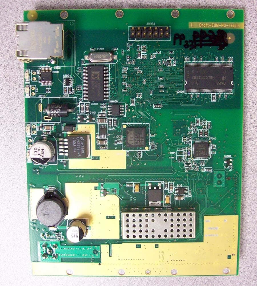
OOX-915C
Oct 23, 2007Wireless Transceiver Module
Equipment Class
DTS - Digital Transmission System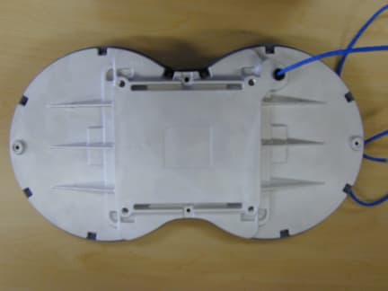
OOX-E3K6
May 10, 2006Outdoor Modem
Equipment Class
DTS - Digital Transmission System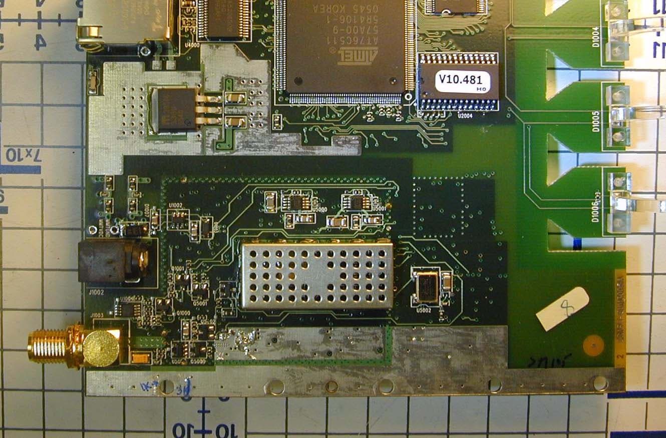
OOX-915A
Mar 27, 2006Radio Module
Equipment Class
DTS - Digital Transmission System
OOX-EUM3005
Mar 21, 2005Wireless Modem
Equipment Class
DTS - Digital Transmission System
OOX-EUM3004
Nov 10, 2003Wireless LAN end-users modem
Equipment Class
DTS - Digital Transmission System