P4YSAM-CRM-12Uni-Pay SAM-CRM-12
Samsung SDS Co., Ltd.
Click to zoom
Application Details
- Equipment Class
- JBP - Part 15 Class B Computing Device Peripheral
- Date of Grant
- Dec 17, 2012
- Application Purpose
- Original Equipment
- Date of Application
- Dec 17, 2012
- Equipment Note
- Uni-Pay SAM-CRM-12
- Company
- Samsung SDS Co., Ltd.
- Country
- South Korea
Documents & Files
Document Text
Text extracted from the exhibit documents filed with the FCC. Open a document above to read the original.
Users Manual
http://www.emc2000.co.kr FCC TEST REPORT EMC compliance Ltd. Page: 1 of 1 480-5 Shin-dong, Yeongtong-gu, Suwon-city, Gyunggi-do, 443-390, Korea 82 31 336 9919 (Main) 82 31 336 4767 (Fax) This test report shall not be reproduced except in full, Without the written approval. Appendix 6. User manual RevisionDateDocument NameDocument NumberPage A42012.11.05SAM-CRM-12 H/W Spec. 1 of 11 SAM-CRM-12(ValidatorPCI)Board H/W Specification 2012. 11. 05 SAMSUNG SDS ______________________________ Project Manager ___________________________ Approved RevisionDateDocument NameDocument NumberPage A42012.11.05SAM-CRM-12 H/W Spec. 2 of 11 Revision History VersionDate Author VerifierDescription RevisionDateDocument NameDocument NumberPage A42012.11.05SAM-CRM-12 H/W Spec. 3 of 11 1Overview SAM-CRM-12(Product name : Uni-Pay) is a PCI-PED Compliant Debit PIN Pad, which supports as following EMV and PCI PTS V3.1. Mag-stripe function. It has TFT LCD which can be used for video advertisement, and host interface via RS232, RS422. 1.1Purpose It isDebit PIN Padmainly use for credit card transaction at automatic ticket vending machine. 1.2Communication & Operation HOST server controls this reader via TCP/IP or RS232, RS422. It receives transaction amount and transaction result from the host. 1.3Functions 1)Contact Card 2)Magnetic Card 3)BUZZER 4)LCD 5)Touch Screen 6)RS-232 communication 7)TCP/IP communication 1.4Certifications (Factions) 1)PCI-PTS The payment card industry (PCI) denotes the debit, credit, prepaid, e- purse, ATM, and POS cards and associated businesses. PCI-PTS was specifically designed to protect consumer PIN data from theft. It is also intended to enforce hardware security of devices that accept consumer PINs and house secret encryption keys of the acquirer, including how the PIN Entry Device (PED) is produced, controlled, transported, stored and used throughout its life cycle. RevisionDateDocument NameDocument NumberPage A42012.11.05SAM-CRM-12 H/W Spec. 4 of 11 2)EMV EMV stands for Europay, MasterCard and VISA, a global standard for inter- operation of integrated circuit cards (IC cards or "chip cards") and IC card capable point of sale (POS) terminals and automated teller machines (ATMs), for authenticating credit and debit card transactions. The EMV standards define the interaction at the physical, electrical, data and application levels between IC cards and IC card processing devices for financial transactions. There are standards based on ISO/IEC 7816 for contact cards, and standards based on ISO/IEC 14443 for contactless cards. RevisionDateDocument NameDocument NumberPage A42012.11.05SAM-CRM-12 H/W Spec. 5 of 11 2Summary Following is the power & communication interface of Uni-Pay (SAM-CRM-12). ITEMSpecificationDescription PowerDC 12V, 1A IN/OUT Interface RS232 2ch, Ethernet 1ch, USB 1ch CertificationEMV, PCI PTS, J/Smart, CE, FCC, UL Internal Main Board divided to sector, one is User interface and the other is Pin input & Communication security. Following is the contents of each sector 2.1User Interface(LCD) ITEMSpecificationDescription Processor 32Bits Microcontroller, ARM Cortex A8, 633MHzModel No. : S5PC100 OSAndroid 2.1Linux 2.6.2.9 kernel Memory SDRAM 256MByte, NAND Flash 512Mbyte (Bios Area + Application Area) LCD4.3 TFT Color LCD, 480*272 pixels IN/OUT Interface RS232 1ch(internal Debug), RS232 1ch(RF Device) or RS485 1ch(External Device) USB2.0 1ch(Debug) I/O Ports for USIP communication Others Audio Speaker, SD Card Slot 2.2PIN Input & Communication security (Touch sensor & Smart Card Control) ITEMSpecificationDescription Processor 32Bits Secure Microcontroller, 96MHz OSLinux RevisionDateDocument NameDocument NumberPage A42012.11.05SAM-CRM-12 H/W Spec. 6 of 11 MemorySRAM 128KByte, Flash 256KByte, OTP 256Byte, ROM 128KByte external Flash 16Mbyte, external SDRAM 32Mbyte external SRAM 16Mbyte TouchTouch Panel(SPI) Smart Card Contact 1 Slot (UART) IN/OUT Interface RS232 2ch(External Device) Ethernet SPI for TOUCH I/F MSRMag-Stripe Reader (UART) Battery Lithium Manganese Dioxide BatteryFor RTC and External Sensors OthersBuzzer CertificationEMV, PCI PTS, CE, FCC, UL RevisionDateDocument NameDocument NumberPage A42012.11.05SAM-CRM-12 H/W Spec. 7 of 11 3Structure The Structure of equipment RevisionDateDocument NameDocument NumberPage A42012.11.05SAM-CRM-12 H/W Spec. 8 of 11 4Description of Surface The picture of device surface Communication Cable LAN or Serial cable The size of terminal 135.5(W) * 152.7(L) * 26(H)mm Mag-stripe Contactcard slot TFT-LCD RevisionDateDocument NameDocument NumberPage A42012.11.05SAM-CRM-12 H/W Spec. 9 of 11 5Connector Pin Assignment 5.1J19 (Connector) NoDescriptionNoDescription 1 POWER (12V)2 GND 3 POWER (12V)4 GND 5 RESET-6 RS485P 7 RESET+8 RS485M 9 TX0_RS23210 TX1_RS232 11 RX0_RS23212 RX1_RS232 13 USB D+14 GND 15 USB D-16 USB_POWER(5V) 17 LAN_RDP18 LAN_TDP 19 LAN_RDM20 LAN_TDM 5.2J6– External cable : Serial and Reset NoDescriptionNoDescription 1 PWR_IN6 - 2 GND7 - 3 TX_RS2328 IO 4 RX_RS2329 RESET+ 5 GND10 RESET- RevisionDateDocument NameDocument NumberPage A42012.11.05SAM-CRM-12 H/W Spec. 10 of 11 6Description of Electricity The Description of power -Input power : 12V The using electric current -Normal 12V, 500mA under -MAX 12V, 700mA under The Description of Serial communication -115200bps, 8 data, no parity, 1 stop bit 7Property Operating Condition -Temperature to use : -10 ~ 70°C -Humidity to use : 50 ~ 95 % (relative humidity) Storage Condition -Temperature to keep : -30 ~ 80°C -Humidity to use : 30 ~ 90 % (relative humidity) 8Warning and Notice -For indoor use only. -This product is affected by an element like metal or Magnetism. So one has to take precautions. RevisionDateDocument NameDocument NumberPage A42012.11.05SAM-CRM-12 H/W Spec. 11 of 11 9Certifications EU This product is CE marked according to the provision of the R&TTE Directive (99/5/EC). Here by DUALi Inc. declares that this product is in compliance with the essential requirements and other re…
Text truncated - open the document above for the full version.
Block Diagram
http://www.emc2000.co.kr FCC TEST REPORT EMC compliance Ltd. Page: 1 of 1 480-5 Shin-dong, Yeongtong-gu, Suwon-city, Gyunggi-do, 443-390, Korea 82 31 336 9919 (Main) 82 31 336 4767 (Fax) This test report shall not be reproduced except in full, Without the written approval. Appendix 4. Block Diagram Copyright ⓒ 2012 Samsung SDS Co., Ltd. All rights reserved | Confidential 1 of 1 시스템 시스템시스템 시스템 개요 개요개요 개요 개 개개 개 요 요요 요 시스템 개요 및 구성도 ‘ Figure 1 시스템 시스템시스템 시스템 구성도 구성도구성도 구성도 None Secure MCU Module (ARM Cortex A8) RF(PORT) Smart Card (Mash *2) RS485 SD Memory Sound RS232*2 RS232*2 PORTS Secure MCU (USIP) Touch pad M/S Reader SAM-CRM-13 (Card Reader) RS232/RESET,/PORT/POWER NOR FLASH SDRAM SRAM LAN Connector Board RS485 / RS232*2 / RESET / POWER / LAN / USB SECURE AREA RESET Validator -PCI RF(RS232) TFT LCD(4.3” USB USB NAND FLASH DDR SDRAM Removal Sensor (LCD / Device) Power Sensor Mash Sensor (PCB / Wall / Cover) Case Open Sensor
External Photos
kwws=22zzz1hpf53331fr1nu EMCComplianceLtd. 480-5 Sin-dong, Yeongtong-gu, Suwon-city, Gyeonggi-do, 443-390, Korea TEL: 82 31 336 9919 FAX: 82 505 299 8311 This test report shall not be reproduced, except in full, without the written approval. Report No.: EMC-2012/057 Page: 17 of 28 7. E.U.T. photographs Front View Rear View kwws=22zzz1hpf53331fr1nu EMCComplianceLtd. 480-5 Sin-dong, Yeongtong-gu, Suwon-city, Gyeonggi-do, 443-390, Korea TEL: 82 31 336 9919 FAX: 82 505 299 8311 This test report shall not be reproduced, except in full, without the written approval. Report No.: EMC-2012/057 Page: 19 of 28 Port
ID Label/Location Info
kwws=22zzz1hpf53331fr1nu EMCComplianceLtd. 480-5 Sin-dong, Yeongtong-gu, Suwon-city, Gyeonggi-do, 443-390, Korea TEL: 82 31 336 9919 FAX: 82 505 299 8311 This test report shall not be reproduced, except in full, without the written approval. FCC ID: P4YSAM-CRM-12 Report No.: EMC-2012/057 Page: 18 of 28 Label FCC Label Location
Internal Photos
kwws=22zzz1hpf53331fr1nu EMCComplianceLtd. 480-5 Sin-dong, Yeongtong-gu, Suwon-city, Gyeonggi-do, 443-390, Korea TEL: 82 31 336 9919 FAX: 82 505 299 8311 This test report shall not be reproduced, except in full, without the written approval. Report No.: EMC-2012/057 Page: 20 of 28 Inside kwws=22zzz1hpf53331fr1nu EMCComplianceLtd. 480-5 Sin-dong, Yeongtong-gu, Suwon-city, Gyeonggi-do, 443-390, Korea TEL: 82 31 336 9919 FAX: 82 505 299 8311 This test report shall not be reproduced, except in full, without the written approval. Report No.: EMC-2012/057 Page: 21 of 28 Main Board kwws=22zzz1hpf53331fr1nu EMCComplianceLtd. 480-5 Sin-dong, Yeongtong-gu, Suwon-city, Gyeonggi-do, 443-390, Korea TEL: 82 31 336 9919 FAX: 82 505 299 8311 This test report shall not be reproduced, except in full, without the written approval. Report No.: EMC-2012/057 Page: 22 of 28 LCD kwws=22zzz1hpf53331fr1nu EMCComplianceLtd. 480-5 Sin-dong, Yeongtong-gu, Suwon-city, Gyeonggi-do, 443-390, Korea TEL: 82 31 336 9919 FAX: 82 505 299 8311 This test report shall not be reproduced, except in full, without the written approval. Report No.: EMC-2012/057 Page: 23 of 28 kwws=22zzz1hpf53331fr1nu EMCComplianceLtd. 480-5 Sin-dong, Yeongtong-gu, Suwon-city, Gyeonggi-do, 443-390, Korea TEL: 82 31 336 9919 FAX: 82 505 299 8311 This test report shall not be reproduced, except in full, without the written approval. Report No.: EMC-2012/057 Page: 24 of 28 Touch Board kwws=22zzz1hpf53331fr1nu EMCComplianceLtd. 480-5 Sin-dong, Yeongtong-gu, Suwon-city, Gyeonggi-do, 443-390, Korea TEL: 82 31 336 9919 FAX: 82 505 299 8311 This test report shall not be reproduced, except in full, without the written approval. Report No.: EMC-2012/057 Page: 25 of 28 SUB Board#1 kwws=22zzz1hpf53331fr1nu EMCComplianceLtd. 480-5 Sin-dong, Yeongtong-gu, Suwon-city, Gyeonggi-do, 443-390, Korea TEL: 82 31 336 9919 FAX: 82 505 299 8311 This test report shall not be reproduced, except in full, without the written approval. Report No.: EMC-2012/057 Page: 26 of 28 SUB Board#2 kwws=22zzz1hpf53331fr1nu EMCComplianceLtd. 480-5 Sin-dong, Yeongtong-gu, Suwon-city, Gyeonggi-do, 443-390, Korea TEL: 82 31 336 9919 FAX: 82 505 299 8311 This test report shall not be reproduced, except in full, without the written approval. Report No.: EMC-2012/057 Page: 27 of 28 Connector Board kwws=22zzz1hpf53331fr1nu EMCComplianceLtd. 480-5 Sin-dong, Yeongtong-gu, Suwon-city, Gyeonggi-do, 443-390, Korea TEL: 82 31 336 9919 FAX: 82 505 299 8311 This test report shall not be reproduced, except in full, without the written approval. Report No.: EMC-2012/057 Page: 28 of 28 Cable#1 Cable#2
Operational Description
Samsung S5PC100 ARM Cortex A8 based Mobile Application Processor S5PC100 Block Diagram From smartphones to personal navigation devices, the Samsung ARM Cortex A8-based S5PC100 Mobile Application Processor supports the requirements of a broad array of applications. The S5PC100 enables the integration of various functionalities, such as, wireless communication, personal navigation, camera, portable gaming, portable music/video player, mobile TV and PDA into one device. The S5PC100 adopts a 32-bit ARM Cortex A8 RISC microprocessor and a 64/32-bit internal bus architecture, and operates up to 833MHz. High Definition Multi Format Codec enables higher resolution multimedia functions at low power consumption High-quality video playback is fast becoming a must-have feature for smartphones, portable media players, GPS navigation units, and TV-enabled mobile devices. The S5PC100 processor features a built-in, 720p multi format codec (MFC) video Engine which ensures smooth 30fps video encoding and playblack at low power consumption, and supports three types of TV out interface (NTSC/PAL/HDMI). Products incorporating the S5PC100 will benefit from the rich video and multimedia functions which consumes very low power, enabling longer video playback time with a standard size battery: •720P quality video capture and playback both at 30fps •High quality real-time video conferencing •MPEG4 (SP/ASP) / H.263 (Profile3) / H.264 (BP/MP/HP) encode & decode •VC1 (SP/MP/AP) decode System Peripheral Timers PLLx4 DMA (32ch) Keypad (8 x 8) ADC & Touch Screen TFT LCD Controller w/DSI 24 / 18bit TFT-LCD 8bit for Dual i80 Virtual Screen Secure RAM Crypto ENGINE Secure ROM Multi - Layer AHB/AXI Bus Connectivity 24bit IIS Dolby 5.1 2 x IIS/AC97/PCM 2 x S/PDIF 4 x UART IrDA v1.1 2xI 2 C 3 x HS-SPI MIPI-HSI/Moderm I/F USB Host 1.1/OTG 2.0 3 x HS-MMC-SD CortexA8 32KB/32KB I/D Cache 667/833MHz Multimedia Acceleration Camera IF w/ CSI-2 720p Video Engine 2D/3D Graphics NTSC/PAL/HDMI JPEG CODEC Memory Interfaces SRAM / ROM / NOR / OneNAND mDDR / DDR2 OneDRAM LPDDR400 / LPDDR2 MLC Flash w/ 8-bit ECC CFII (ATA) 256KB L2 Cache NEON •San #24 Nongseo-Dong, Kiheung-Gu, Yongin-City, Kyunggi-Do, Korea• TEL: 82-31-209-1965 • FAX: 82-31-209-1919 - For more information please contact•E-mail: [email protected]•URL: http://www.samsungsemi.com •San #24 Nongseo-Dong, Kiheung-Gu, Yongin-City, Kyunggi-Do, Korea• TEL: 82-31-209-1965 • FAX: 82-31-209-1919 - For more information please contact•E-mail: [email protected]•URL: http://www.samsungsemi.com • The appearance of all products, dates, figures, diagrams and tables are subject to change at any time without notice. Samsung S5PC100 ARM Cortex A8 based Mobile Application Processor Additional S5PC100 Advantages The S5PC100 mobile application processor provides a cost-effective, low power, high-performance solution for any portable designs: • Cortex A8 Based Application Processor:The S5PC100 is a highly optimized ARM Cortex A8 based application processor targeted for low power portable designs. The ARM subsystem includes separate 32KB Instruction and 32KB data caches, 256KB L2 caches, as well as a full MMU to handle virtual memory management. The Cortex A8 also provides support for JAVA acceleration, and includes a dedicated vector floating point coprocessor allowing efficient implementation of various encryption schemes and high quality 3D graphics applications. Optimized interface for high memory bandwidth requirements:The S5PC100 has an optimized interface to externalmemory capable of sustaining the demanding memory bandwidths required in high-end communication services. The memory system support mDDR / DDR2 / LPDDR2 of 200MHz which is enough bandwidth to cover XVGA display with 720p video decoding. Flash/ROM Port supports NAND Flash (MLC and SLC), NOR-Flash, OneNAND, ROM type external memory as well as, Samsung newly unveiled memory, MoviNAND. Additionally, it supports booting from MoviNAND. Software support to reduce application design time:Existing applications on Samsung application processor families can be ported to the S5PC100 application processors with minimal changes to the BSP. Different operating systems (such as Windows CE, Windows Mobile, Linux ® ,and Symbian), are supported on the S5PC100, enabling manufacturers and mobile operators to differentiate their products through a rich, easy-to-use and customizable user interface, and a robust and flexible application architecture. Rich peripherals to reduce total system BOM cost and enhance overall functionality:To reduce total system cost and enhance overall functionality, the S5PC100 includes many hardware peripherals; TFT 24-bit true color LCD controller, HDMI Interface, CF+, ATA I/F, 32-channel DMA, Dedicated IrDA port for FIR, MIR and SIR, AC-97 audio Codec interface, USB 2.0 OTG operating at high speed, SD Host & High Speed Multi-Media Card Interface and Touch Screen Panel (TSP) ADC. By integrating these system peripherals and analog blocks on chip, the S5PC100 minimizesoverall system costs and eliminates the need of many costly external components. The S5PC100 further lowers the cost of system memory storage by supporting Multi-level Cell (MLC) NAND Flash, allowing more functionality andpersonalization options which requires high volume storage. Support OneDRAM:Next generation smartphone which incorporates the S5PC100 can leverage Samsung OneDRAM to further reduce the system BOM cost by sharing the OneDRAM memory between the S5PC100 and the modem, eliminating the standalone memory normally needed to support the modem operation. Memory stacking options for smaller footprints:The S5PC100 can be combined with various memory choices via Package-on-Package (POP) or Multiple-Chip-Package (MCP) • • • • •
Operational Description
USIP Universal Secure Integrated Platform Universal Secure Integrated Platform for trusted terminals Professional IC ZI Athélia II - Avenue Coriandre - 13704 La Ciotat Cedex - France Tel : + 33 (0) 4 42 98 14 80 – Fax : + 33 (0) 4 42 08 33 19 – E-mail : [email protected] www.innova-card.com ® USIP ® Professional IC actual size : 15 x 15 mm USIP ® Professional ICis a secure System on Chip (SoC) providing all the functionalities required to build new generations of trusted terminals and readers. USIP ® Professional ICis dedicated to applications that need a high level of security and confidentiality such as financial transactions and payment (EMV and GP/STIP), healthcare, identity, access control, mobile applications, Pay TV, biometry. Main Features ■ MIPS ® 4KSd™ 32-bit RISC processor ■ Embedded memories (SRAM, ROM, Flash) ■ Patented security and cryptographic features ■ Controllers, analog and digital interfaces (smart card, USB, SPI, etc) ■ Power Management Benefits ■ Offers Single-Chip Solution ■ Reduces drastically the Bill of Materials ■ Facilitates Certification (EMV PCI PED compliance) ■ Speeds up Time To Market ■ Enables Migration to Open Platforms ■ Enables new Form Factor Devices PLL VbattVbatt VbattVbatt 12 MHz12 MHz *UCI: USIP ® Crypto Interface **USN: Unique Serial Number *UCI: USIP ® Crypto Interface **USN: Unique Serial Number 1,8 V/3,3 V1,8 V/3,3 V 6060 55 55 55 2424 1111 UMC Smart Card Controller 0 Smart Card Controller 1 Smart Card Controller 2 UCI* AES 128 bits Up to 12 x 12 Matrix keyboard Controller LCD Interface Secure 32-bit Processor MIPS32 ® 4KSd ™ SRAM UART 0 RS232/Irda UART 1 Modem UART 2 UART 3 USB 2.0 OTG Interrupt Controller USART SPI USART I2C GPIO Parallel Interface ADC-10 bits PS/2 PWM 1 PWM 2 F2F Decoder up to 3 tracks (Map Stripe) Thermal Printer Interface FLASH Noise Generator Timers / Counters Watchdog Battery Powered Keys Secure Real Time Clock DMA Controller (1D/2D) True RNG Internal Sensors Sensors Intput ROM USN** I-Cache 8 kBytes - 4 ways 128 kBytes 256 kBytes 128 kBytes 512 bits Configurable OTP (HAL + Secure Boot Loader) FIREWALL D-Cache 8 kBytes - 4 ways MMU Power Consumption Management Tamper Protection 22 88 22 22 44 11 77 22 3232 1717 1111 66 22 33 11 11 1212 I/OI/OCoreCore DMADMA 32,768 KHz32,768 KHz 1,8 1,8 ResetReset USIP Universal Secure Integrated Platform ® Innova Card is a semiconductor fabless company that designs complex Systems on Chip and supplies secure hardware and software solutions for trusted terminals. By extending the secure smart card technology onto chips for terminals, Innova Card offers the most secure and integrated circuit called: USIP ® Professional IC. 32-bit RISC Processor ■ USIP ® Professional ICembeds the MIPS32 ® 4KSd™ secure processor from MIPS ® Technologies. ■ It is a high-performance, low-power core designed for custom system-on-silicon applications. Main characteristics ■ 1.35 MIPS/MHz (Dhrystone) 129,6 MIPS@96MHz ■ Specific instruction set for cryptographic applications (smart MIPS) ■ 8 KByte data cache and 8 KByte instruction cache memories ■ 5-Stage Pipeline ■ 16-bit code compression via MIPS16e™ ASE Memories ■ 128 KBytes of SRAM ■ 128 KBytes of ROM ■ 256 KBytes of Flash Memory with locked features ■ 256 Bytes of OTP ■ Universal Memory Controller (UMC) to manage external SRAM/SDRAM/Flash Memory (1.8V or 3.3V supported) Security Aspects ■ USIP ® Professional ICprovides developers with a large set of security features that facilitates software developments for secure applications and enhances the security level. ■ Secure Memory Management Unit (MMU): protection of pages individually programmable (execute, read, and write) – 1KByte of granularity ■ Unique chip Serial Number (USN) ■ USIP ® Crypto Interface (UCI): efficient on-the-fly encryption of memories based on the NIST FIPS-197 Standard AES ■ Firewall for USB Access ■ Protected Storage Area ■ Tamper protection, internal sensors (voltage, frequency, temperature, active metal shield) and external sensors input – also operate in power down mode ■ True Random Number Generator: NIST and DIEHARD tests passed ■ AES crypto processor ■ Secure Boot Loader with dynamic authentication based on AES Controllers, analog and digital Interfaces ■ 3 reversible smart card controllers: ISO-7816 (T=0 and T=1) UARTs with EMV Level 1 driver. They are able to manage up to 10 smart cards ■ 3 channels F/2F decoder: digital part of the Magnetic Stripe Reader interface (up to 3 tracks supported and two-way reading) ■ Thermal printer interface: it can drive any thermal print head in serial mode. It includes the stepper motor control ■ Secure Real Time Clock powered by an independant battery ■ Keyboard controller: a 12x12 Matrix Keyboard interface with hardware scanning and debouncing features ■ LCD interface ■ DMA controller ■ Communication interfaces: USB OTG 2.0 full speed, UARTs, UART Modem, SPI master / slave, I2C master / slave, Parallel, PS2, IrDA/UART ■ General purposes: 32 GPIOs, 2 PWMs, Watchdog, 4 Timers/Counters, 6 ADC inputs (10-bit resolution) Power Management ■ Dynamic Frequency Management from 12 to 96 MHz ■ Low Power Core Consumption ■ Gated Clock on each block ■ Power Supply Supervisor ■ Interrupt Based System ■ Running / Idle / Power Down Modes © 2005 Innova Card – Innova Card makes no warranty for the use of its products, other than those expressly contained in the general terms for use. No licenses to patents or other IPs of Innova Card are granted with the sale of Innova Card’s products. The company assumes no responsibility for any errors which may appear in this document, and reserves the right to make changes in specifications and devices described herein at any time without notice. Therefore, the reader has to make sure that the flyer is current before placing orders. Innova Card ® and USIP ® are registered trademarks of Innova Card. Graphic Design : www.bruno-r.com Product Features Block Diagram of USIP ® Professional IC ZI Athélia II - Avenue Corian…
Text truncated - open the document above for the full version.
Schematics
http://www.emc2000.co.kr FCC TEST REPORT EMC compliance Ltd. Page: 1 of 1 480-5 Shin-dong, Yeongtong-gu, Suwon-city, Gyunggi-do, 443-390, Korea 82 31 336 9919 (Main) 82 31 336 4767 (Fax) This test report shall not be reproduced except in full, Without the written approval. Appendix 5. Schematics Circuit설명 File NamePCB NameRemark MCUC100_(CircuitDiagram).pdfMCU PCB SAM-CRM-12_Main_(CircuitDiagram).pdf Main PCB SAM-CRM-12_SUBs_(CircuitDiagram).pdf SC PCBPage 1 Wall-C2,3Page 2 / 2ea Wall-C1Page 3 Cover PCBPage 4 Wall-A1,2,3 Page 5 /3ea Wall-D1,2,3,4 Page 6 /3ea / D1,D2는 동일 Wall-B1,2,3 Page 7 / 3ea / B1,B2는 동일 SAM-CRM- 12_Connector_(CircuitDiagram).pdf Connector PCB MCUC100_(CircuitDiagram) 55 44 33 22 11 D D C C B B A A XOM4XOM0XOM1XOM3XOM2XBO3XBO1XBO4XBO0XBO2XBO5 XOM1XBO5XOM0XOM2XBO0XOM3XOM4XBO1XBO4XBO2 XjTRSTn XnRESET XjTRSTnXjTDIXjTMSXjTCKXi2cSDA0Xi2cSCL0 Xi2cSDA1/SPDIF_OUTXi2cSCL1/SPDIF_CLK XBO3 VDD_INT_AP VDD_3.3V VDD_3.3V VDD_3.3V VDD_3.3V VDD_3.3V XiemSCLK 8 XspiCS1 8 XuRTSn0 8 XuTXD2 8 XspiMISO1 8 XuhDP 8 XPWRRGTON 7,8 XspiCS0 8 XpwmTOUT2/DMA_ACKn 8 XuCTSn0 8 XpwmTOUT1/DMA_REQn 8 XuCLK/IRDA_SDBW 8 X27MXTOXrtcXTO XuRTSn1 8 XspiMISO0 8 XuRXD3/CTSn2/IRDA_RXD 8 XuoDP 8 XusbXTI XuTXD1 8 XjTDO 8 XspiCLK0 8 XpwmTOUT0/TCLK 8 XspiMOSI1 8 XuTXD0 8 XXTO XuoDM 8 XuTXD3/RTSn2/IRDA_TXD 8 XspiMOSI0 8 XspiCLK1 8 XiemSPW I 8 XuhDN 8 XuRXD2 8 XmmcDATA2_2/PCM_SOUT0/I2S_SDO2 8 XusbXTO XuoID 8 XuCTSn1 8 XmmcDATA0_2 8 Xi2cSDA1/SPDIF_OUT 8 XmmcDATA0_4 8 Xi2cSDA0 8 XmmcDATA0_0 8 Xi2sCDCLK1/PCM_EXTCLK1/AC97_RESETn 8 Xi2sCLK0 8 XmmcDATA2_3/SPDIF_OUT 8 Xi2sLRCK1/PCM_FSYNC1/AC97_SYNC 8 XmmcDATA1_1 8 Xi2sCDCLK0 8 Xi2sLRCLK0 8 XmmcDATA2_1/PCM_SIN0/I2S_SDI2/SPI_MOSI2 8 XmmcDATA0_1 8 XmmcDATA0_3 8 XmmcDATA1_0 8 Xi2sSDO1/PCM_SOUT1/AC97_SDO 8 XmmcDATA1_2 8 XmmcCMD2/PCM_EXTCLK0/I2S_CDCLK2/SPI_CSn2 8 XmmcDATA0_7 8 XmmcCLK0 8 Xi2cSCL0 8 XmmcDATA2_0/PCM_FSYNC0/I2S_LRCK2/SPI_MISO2 8 XmmcDATA1_3 8 XmmcDATA0_5 8 XmmcCLK2/PCM_SCLK0/I2S_SCLK2/SPI_CLK2 8 Xi2sSDO0_0 8 XmmcCMD1 8 Xi2sSDO0_2 8 XmmcCLK1 8 Xi2sCLK1/PCM_SCLK1/AC97_BITCLK 8 XmmcCMD0 8 Xi2cSCL1/SPDIF_CLK 8 Xi2sSDO0_1 8 XmmcDATA0_6 8 XuoDRVVBUS 8 XnBATF 7XEINT28/KP_ROW 4/CAN_TX0 8 XEINT24/KP_ROW 0/CAMB_PCLK 8 XjTDI 8X27MXTIXEINT22/KP_COL6/CAMB_D6 8 XEINT13/CG_GPO1 8 XjTMS 8XXTIXEINT9XEINT20/KP_COL4/CAMB_D4 8 XEINT14/CG_GPO2 8 XnRESET 8XEINT30/KP_ROW 6/CAN_TX1 8 XEINT29/KP_ROW 5/CAN_RX0 8 XEINT27/KP_ROW 3/CAMB_FIELD 8 XEINT25/KP_ROW 1/CAMB_VSYNC 8 XEINT31/KP_ROW 7/CAN_RX1 8 XrtcXTIXEINT11/CG_IMGIN 8 XuRXD1 8 XEINT26/KP_ROW 2/CAMB_HREF 8 XEINT23/KP_COL7/CAMB_D7 8 XuRXD0 8 XEINT16/KP_COL0/CAMB_D0 8 XEINT18/KP_COL2/CAMB_D2 8 XEINT17/KP_COL1/CAMB_D1 8 XjTCK 8XjTRSTn 8XEINT10/CG_REALIN 8 XEINT19/KP_COL3/CAMB_D3 8 XEINT15/CG_GPO3 8 XEINT12/CG_GPO0 8 XEINT21/KP_COL5/CAMB_D5 8 Xi2sSDI1/PCM_SIN1/AC97_SDI 8 XmmcCDn1 8 XuoVBUS 8 CG_CLK 8 Xi2sSDI0 8 XmmcCDn2/SPDIF_CLK 8 XmmcCDn0 8 XOM2 8 XBO0 8XBO5 8 X27MXTI XrtcXTI XXTI XusbXTI XrtcXTO X27MXTO XusbXTO XXTO XnRSTOUT 8XEINT0/GPH0_0 8 XEINT1/GPH0_1 8 XEINT2/GPH0_2 8 XEINT3/GPH0_3 8 XEINT4/GPH0_4 8 XEINT5/GPH0_5 8 XEINT6/GPH0_6 8 XEINT7/GPH0_7 8 XEINT8/GPH0_8 8 XjTDI 3 XjTRSTn 3 XjTMS 3 XjTCK 3 XjTDO 3 XnRESET 3 NFMODE No ECC Encryption USB Booting 0 : XxTI, XxTO1 : XusbXTI, XusbXTO (Reserved)(Reserved) BootingMode OptionSelection BO[3:0] PLL Clock Source 0 ECC Encryption BO[2:0] 0 3Cycle(512B),4Cycle(2~4KB) 0 1 1 OM[3:1] 0 0 2KB Page Movi/i-NAND Description 1 i NAND(SD) 11 512Byte Page 1 0 1 OM[4,0] iROM Boot 1 iROM Boot 0 0 0 Description 0 0 OneNAND [3] - 0 BO[5:4] iROM Boot 0 4KB Page 0 1st Boot 1 0 MoviNAND(MMC) NAND/xD 1 Description 0 1 1 1 0 1 1 0 0 4Cycle(512B),5Cycle(2~4KB) 1 OM[0] 1 OM[4] 0 2nd Boot 1 1 0 1 521 PinFCFBGA X-Tal Clock Source For APLL,MPLL,EPLL(Inc.USBHost) + USB OTG For APLL,MPLL,EPLL(Inc.USBHost) For RTC For DAC/HDMI 2010.12.29 APPROVE SIGN PAGE MODEL DE-MCUC100 3 DATE CHECK DRAW DOC. NO 8 EP06-10-016 X327MHz/SX32X327MHz/SX32 1 3 2 4 R9 5.1M/R1005 R9 5.1M/R1005 R39 100K/R1005 R39 100K/R1005 R11 10K/R1005 R11 10K/R1005 R61M/R1005R61M/R1005 R22 220R/R1005 R22 220R/R1005 R40 100K/R1005 R40 100K/R1005 R270/R1005R270/R1005 R32 100K/R1005 R32 100K/R1005 C315pF/C1005C315pF/C1005 R38 100K/R1005 R38 100K/R1005 R4 10K/R1005/xxx R4 10K/R1005/xxx C722pF/C1005C722pF/C1005 TP1 XCLKOUT TP1 XCLKOUT R23 2K/R1005 R23 2K/R1005 R51M/R1005R51M/R1005 X112MHz/SX32X112MHz/SX32 1 3 2 4 R20 2K/R1005 R20 2K/R1005 C215pF/C1005C215pF/C1005 C813pF/C1005C813pF/C1005 R37 100K/R1005 R37 100K/R1005 R10 10K/R1005 R10 10K/R1005 R280/R1005R280/R1005 R81M/R1005R81M/R1005 R1410K/R1005/NLR1410K/R1005/NL R36 100K/R1005 R36 100K/R1005 R13 10K/R1005 R13 10K/R1005 R1710K/R1005R1710K/R1005 R30 100K/R1005 R30 100K/R1005 R3 0/R1005 R3 0/R1005 R260/R1005R260/R1005 R290/R1005R290/R1005 R93 0R/R1005 R93 0R/R1005 CON1HDR10X1_125MMCON1HDR10X1_125MM12345678910 R2 0/R1005 R2 0/R1005 X212MHz/SX32X212MHz/SX32 1 3 2 4 R7 44.2/F/R1005 R7 44.2/F/R1005 C613pF/C1005C613pF/C1005 UART/IrDA I2C HS-SPI USBHOST 1.1OTG 2.0 HS-MMC I2S/PCM/AC97 PWM Timer [CLOCK][JTAG] EINTGPS/KEYPAD/CAMB [SYSTEM OPTION][BOOTING OPTION][RESET] SYSTEM [IEM] U1AS5PC100 UART/IrDA I2C HS-SPI USBHOST 1.1OTG 2.0 HS-MMC I2S/PCM/AC97 PWM Timer [CLOCK][JTAG] EINTGPS/KEYPAD/CAMB [SYSTEM OPTION][BOOTING OPTION][RESET] SYSTEM [IEM] U1AS5PC100 XuRXD0/GPA0_0 G26 XuTXD0/GPA0_1 H24 XuCTSn0/GPA0_2 K25 XuRTSn0/GPA0_3 F26 XuRXD1/GPA0_4 H26 XuTXD1/GPA0_5 J24 XuCTSn1/GPA0_6 L25 XuRTSn1/GPA0_7 F27 XuRXD2/GPA1_0 H25 XuTXD2/GPA1_1 H27 XuRXD3/CTSn2/IRDA_RXD/GPA1_2 G27 XuTXD3/RTSn2/IRDA_TXD/GPA1_3 J25 XuCLK/IRDA_SDBW/GPA1_4 J26 Xi2cSDA0/GPD3 L26 Xi2cSCL0/GPD4 F25 XspiMISO0/GPB0 M25 XspiCLK0/GPB1 K27 XspiMOSI0/GPB2 M24 XspiCSn0/GPB3 J27 XspiMISO1/GPB4 N20 XspiCLK1/GPB5 L27 XspiMOSI1/GPB6 M21 XspiCSn1/GPB7 L20 XuhDP AE19 XuhDN AE20 XuoDP AG23 XuoDN AG24 XuoVBUS AE23 XuoID AF21 XuoREXT AF24 XmmcCLK1/GPG2_0 P26 XmmcCMD1/GPG2_1 N25 XmmcDATA1_0/GPG2_2 P25 XmmcDATA1_1/GPG2_3 R25 XmmcDATA1_2/GPG2_4 P27 XmmcDATA1_3/GPG2_5 P24 XmmcCLK0/GPG0_0 L19 XmmcCMD0/GPG0_1 M27 XmmcDATA0_0/GPG0_2 N24 XmmcDATA0_1/GPG0_3 P21 XmmcDATA0_2/GPG0_4…
Text truncated - open the document above for the full version.
Test Report
http://www.emc2000.co.kr EMCComplianceLtd.480-5 Sin-dong, Yeongtong-gu, Suwon-city, Gyeonggi-do, 443-390, Korea TEL: 82 31 336 9919FAX: 82 505 299 8311 This test report shall not be reproduced, except in full, without the written approval. FCC ID: P4YSAM-CRM-12 Report No.: EMC-2012/057 Page: 2 of 33 Contents 1. Applicant information .................................................................................................................................... 3 2. Laboratory information ................................................................................................................................. 4 3. Test system configuration............................................................................................................................... 5 3.1 Operation environment ..................................................................................................................... 5 3.2 Measurement Uncertainty ................................................................................................................. 6 4. Description of E.U.T. ...................................................................................................................................... 7 4.1 General information .......................................................................................................................... 7 4.2 Product description ........................................................................................................................... 8 4.3 Auxiliary equipments ........................................................................................................................ 8 4.4 Test configuration .......…
Text truncated - open the document above for the full version.
Contact Information
Applicant
Myoung Kue Lee(Advisory Engineer)
Test Firm
EMC Compliance Ltdchangmin kim
Technical Specifications
| # | Rule Parts | Frequency Range | Power Output |
|---|---|---|---|
| 1 | 15B | - | - |
Other Applications from Samsung SDS Co., Ltd.
P4YSHP-A30
Jan 16, 2020Digital Doorlock
Equipment Class
DTS - Digital Transmission System
P4YSHP-DS510
Apr 16, 2015Digital door lock
Equipment Class
DXX - Part 15 Low Power Communication Device Transmitter
P4Y365PLUS
Mar 26, 2015Digital door lock
Equipment Class
DTS - Digital Transmission System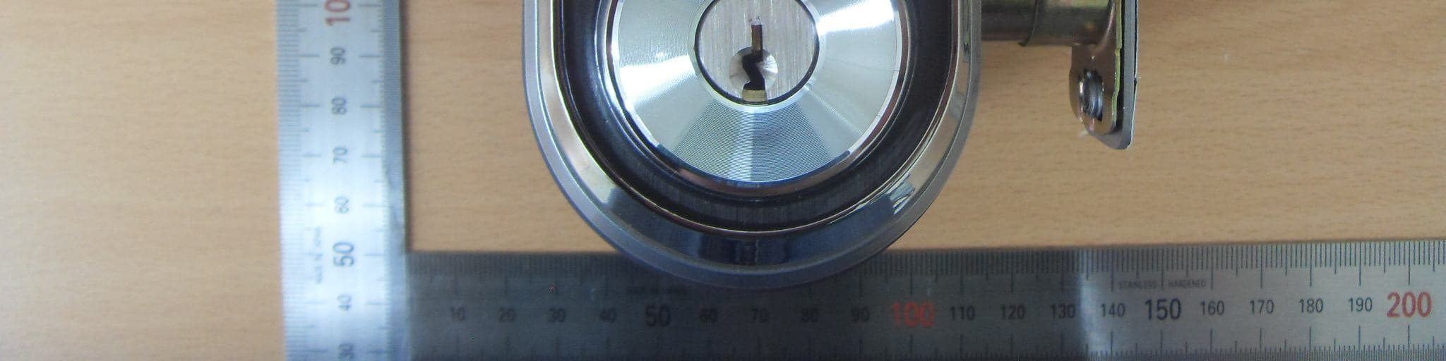
P4YSHN-WDD510
Oct 05, 2014Digital door lock
Equipment Class
DTS - Digital Transmission System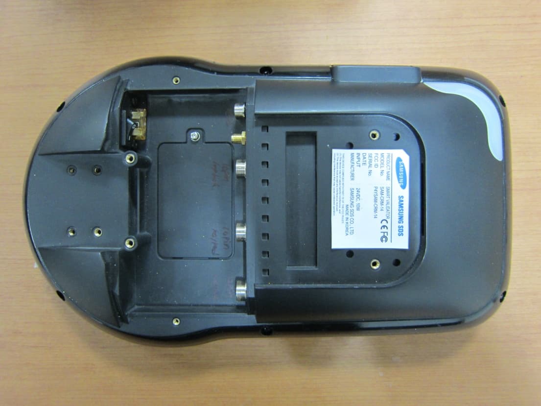
P4YSAM-CRM-14
Jan 19, 2014SMART VALIDATOR
Equipment Class
DSS - Part 15 Spread Spectrum Transmitter