PEQ838A1703061-Channel RF (Rx) in/Remote Thermo Wallclock + RCC
Electronics Tomorrow Ltd.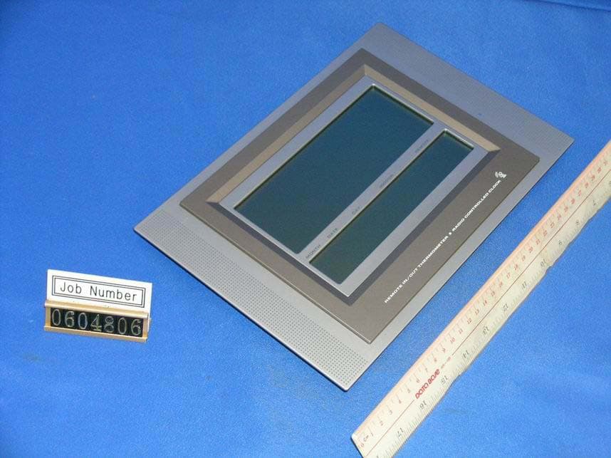
Click to zoom
Application Details
- Equipment Class
- CYY - Communications Receiver used w/Pt 15 Transmitter
- Date of Grant
- Jun 21, 2006
- Application Purpose
- Original Equipment
- Date of Application
- Jun 21, 2006
- Equipment Note
- 1-Channel RF (Rx) in/Remote Thermo Wallclock + RCC
- Frequency Range
- 433.00000000 - 433.00000000
- Company
- Electronics Tomorrow Ltd.
- Country
- Hong Kong
Documents & Files
Document Text
Text extracted from the exhibit documents filed with the FCC. Open a document above to read the original.
Block Diagram
Page 1April 2004 RX3310A UHF ASK Receiver HiMARK Technology, Inc. reserves the right to change the product described in this datasheet. All information contained in this datasheet is subject to change without prior notice. HiMARK Technology, Inc. assumes no responsibility for the use of any circuits shown in this datasheet. Description The RX3310A is a fully integrated, amplitude-shift-keying (ASK) modulation, single chip receiver. It is designed to operate in a variety of low power radio applications. All popular radio frequencies from 250 MHz to 450 MHz may be supported by simply choosing the appropriate external components. Particular emphasis has been placed on low current con- sumption. Features Wide frequency range: 250 MHz to 450 MHz High sensitivity Low power consumption Automotive temperature range High integration level requiring few and inexpensive external components SOP 18L package or SSOP 20L (150 mil) package Applications Remote control systems Car alarm and other security systems Baby finder, wireless doorbell, wireless toys Block Diagram RF AMP MIXER OSC IF FILTER COMPARATOR IF AMP BUFFER LIMITER BANDGAP REFERENCE FO OSC1OSC2 CPA CPBCPO VSSDATADISABLE VCCVEEVIRF VCCLINCPC LFB VORF MIXIN
External Photos
Test Setup FCC ID : PEQ838A170306 External Photo - Front External Photo - Rear
Internal Photos
Test Setup FCC ID : PEQ838A170306 Internal Photo - 1 Internal Photo - 2 Test Setup FCC ID : PEQ838A170306 Internal Photo - 3 Internal Photo - 4 Test Setup FCC ID : PEQ838A170306 Internal Photo - 5 Internal Photo - 6 Test Setup FCC ID : PEQ838A170306 Internal Photo - 7 Internal Photo - 8 Test Setup FCC ID : PEQ838A170306 Internal Photo - 9 Internal Photo - 10 Test Setup FCC ID : PEQ838A170306 Internal Photo - 11
Operational Description
Technical Description of the circuit: This product can be divided into two separate function modules (i) RF module (ii) RCC module (i) RF module This module can be divided into two parts- RF and Baseband; the RF circuit is a single conversion, super-heterodyne architecture receiver IC. The incoming RF signal received by the antenna is fed to the RF input terminal of the IC RX3310A, and then the RF signal is then amplified by the LNA in the IC RX3310A. The amplified signal will fed to the mixer input, the LO for the mixer is generated by the external LC tank circuit, in the above circuit, the LO is 431.12MHz, the IF (F RF –F LO ) is then demodulated by the demodulator in the IC RX3310A and then IC RX3310A provide the raw data. The data is then fed to the Baseband MCU TM8706 for decoding and the MCU TM8706 will display the decoded temperature on the LCD. (ii) RCC module This module can also divide into RF and Baseband, the RF circuit is an AM demodulator, which receive 60kHz WWVB time signal and demodulated by the demodulator in the IC MAS9180A1 and then IC MAS9180A1 provide the useful time data. The data is the fed to the Baseband MCU TM8706 for decode, the decoded time will be display on the LCD. Component Description:Category IC no. (Label) Name Description INTEGRATED CIRCUIT TM8706-K400 Master MCU LCD Driver, RCC Reveiver, Clock and Calender operatio n CRYSTAL 32.768kHz(X2) 15-ppm For Master MCU CRYSTAL 60kHz (X1) 10-ppm For RCC Receiver INTEGRATED CIRCUIT RX3310A (U1) RF Receiver RF Decode INTEGRATED CIRCUIT MAS9180A1(IC1) RCC Receiver RCC Decode Page 1April 2004 RX3310A UHF ASK Receiver HiMARK Technology, Inc. reserves the right to change the product described in this datasheet. All information contained in this datasheet is subject to change without prior notice. HiMARK Technology, Inc. assumes no responsibility for the use of any circuits shown in this datasheet. Description The RX3310A is a fully integrated, amplitude-shift-keying (ASK) modulation, single chip receiver. It is designed to operate in a variety of low power radio applications. All popular radio frequencies from 250 MHz to 450 MHz may be supported by simply choosing the appropriate external components. Particular emphasis has been placed on low current con- sumption. Features Wide frequency range: 250 MHz to 450 MHz High sensitivity Low power consumption Automotive temperature range High integration level requiring few and inexpensive external components SOP 18L package or SSOP 20L (150 mil) package Applications Remote control systems Car alarm and other security systems Baby finder, wireless doorbell, wireless toys Block Diagram RF AMP MIXER OSC IF FILTER COMPARATOR IF AMP BUFFER LIMITER BANDGAP REFERENCE FO OSC1OSC2 CPA CPBCPO VSSDATADISABLE VCCVEEVIRF VCCLINCPC LFB VORF MIXIN RX3310A Page 2April 2004 Package and Pin Assignment: SOP 18L or SSOP 20L Sym bols SOP 18L (dimensions in mm) SOP 18L (dimensions in inch) SSOP 20L (dimensions in mm) SSOP 20L (dimensions in inch) MIN.NOM.MAX.MIN.NOM.MAX.MIN.NOM.MAX.MIN.NOM.MAX. A------2.640------0.1041.351.601.750.0530.0640.069 A10.100------0.004------0.1---0.250.004---0.010 A22.1902.2902.3900.0860.0900.094---1.45------0.057--- b0.3600.4100.4600.0140.0160.0180.200.250.300.0080.0100.012 C0.2420.2500.2580.0070.0100.0130.19---0.250.007---0.010 D11.4611.5611.660.4510.4550.4598.55---8.750.337---0.344 SOP 18L package VCC MIXIN VORF VEE VIRF LFB VCC LIN 18 17 16 15 14 13 12 11 10 CPC OSC1 OSC2 FO CPA CPB CPO VSS DATA 1 2 3 4 5 6 7 8 HiMARK RX3310A 9 DISABLE SSOP 20L package VCC VORF VEE VIRF LFB VCC LIN 18 17 16 15 14 13 12 11 CPC OSC1 OSC2 FO CPA CPB CPO VSS DATA HiMARK RX3310A DISABLE 1 2 3 4 5 6 7 8 9 10 19 20 MIXIN VCC VSS RX3310A Page 3April 2004 RX3310A Chip Window E10.0410.3410.640.3950.4070.4195.80---6.200.228---0.244 E17.3907.4907.5900.2910.2950.2993.80---4.000.150---0.157 e1.2201.2701.3200.0480.0500.052---0.64------0.025--- L0.6400.8401.0400.0250.0330.0410.40---1.270.016---0.050 θ 0 °---8°0°---8°0° --- 8 °0° --- 8 ° y --- ---0.050 --- ---0.002------0.10------0.004 Sym bols SOP 18L (dimensions in mm) SOP 18L (dimensions in inch) SSOP 20L (dimensions in mm) SSOP 20L (dimensions in inch) MIN.NOM.MAX.MIN.NOM.MAX.MIN.NOM.MAX.MIN.NOM.MAX. RX3310A Page 4April 2004 Pin Descriptions Number (18L SOP) Number (20L SSOP) NameI/ODescription 120OSC1IOOscillator tank connection 21OSC2IOOscillator tank connection 32FOOIF filter output 43CPAIComparator input A 54CPBIComparator input B 65CPOIComparator offset adjustment 76,7VSSGNDGround 88DATAOData output 99DISABLEIDisable input. See Electrical Characteristics (cont.) on page 6 1010CPCIComparator input C 1111LINILimiter input 1212VCCPOWERPositive supply voltage 1313LFBIOLimiter feedback B 1414VIRFIRF amplifier input (requires external ac decoupling capacitor) 1515VEEGNDGround for RF amplifier 1616VORFORF amplifier output 1717MIXINIMixer input (requires external ac decoupling capacitor) 1818,19VCCPOWERPositive supply voltage RX3310A Page 5April 2004 Absolute Maximum Ratings V SS = 0 V Recommended Operating Conditions V SS = 0 V ParameterSymbolRatingUnit Supply voltage V CC V SS – 0.3 to V SS + 6.0 V Operating temperature range T OPR –60 to 85 °C Storage temperature range T STG –60 to 125 °C Soldering temperature range T SLD 255 °C Soldering time range t SLD 10s ParameterSymbol Va l u e Unit min.typ.max. Supply voltage range V CC 2.03.06.0V Operating temperature T A –402585 °C RX3310A Page 6April 2004 Receiver Characteristics (V CC = 2.0 to 6.0 V, LO-RF=1.8MHz,All tests at T A = 25 °C unless otherwise noted) Electrical Characteristics (V CC = 3.0 V, V SS = 0 V, All tests at T A = 25 °C unless otherwise noted) Electrical Characteristics (cont.) (V CC = 5.0 V, V SS = 0 V, All tests at T A = 25°C unless otherwise noted) ParameterSymbolCondition Va l u e Unit min.typ.max. Sensitivity P sens V CC = 3.0 V, T A = 27 °C, AM 99%, sine wave (ASK square wave) -100 (-104) -98 (-102) dBm Maximum input powerP in,max -35-30dBm Receiver turn-on timet …
Text truncated - open the document above for the full version.
Test Report
• The test results reported in this test report shall refer only to the sample actually tested and shall not refer or be deemed to refer to bulk from which such a sample may be said to have been obtained. • This report shall not be reproduced except in full without prior authorization from Intertek Testing Services Hong Kong Limited. • For Terms And Conditions of the services, it can be provided upon request. • The evaluation data of the report will be kept for 3 years from the date of issuance. Intertek Testing Services Hong Kong Ltd. 2/F., Garment Centre, 576 Castle Peak Road, Kowloon, Hong Kong. Tel: (852) 2173 8888 Fax: (852) 2371 0521 Website: www.hk.intertek-etlsemko.com Electronics Tomorrow Ltd. Application For Certification (FCC ID: PEQ838A170306) Superheterodyne Receiver 0604806 BC/ Sandy Lee April 24, 2006 INTERTEK TESTING SERVICES FCC ID: PEQ838A170306 i LIST OF EXHIBITS INTRODUCTION EXHIBIT 1: General Description EXHIBIT 2: System Test Configuration EXHIBIT 3: Emission Results EXHIBIT 4: Equipment Photographs EXHIBIT 5: Product Labelling EXHIBIT 6: Technical Specifications EXHIBIT 7: Instruction Manual EXHIBIT 8: Miscellaneous Information INTERTEK TESTING SERVICES FCC ID: PEQ838A170306 ii MEASUREMENT/TECHNICAL REPORT Electronics Tomorrow Ltd. - MODEL: Electronics Tomorrow Ltd. 838A FCC ID: PEQ838A170306 This report concerns (check one:) Original Grant X Class II Change _____ Equipment Type: Superheterodyne Receiver (example: computer, printer, modem, etc.) Deferred grant requested per 47 CFR 0.457(d)(1)(ii)? Yes No X If yes, defer until: date Company Name agrees to notify the Commission by: date of the intended date of announcement of the product so that the grant can be issued on that date. Transition Rules Request per 15.37? Yes No X If no, assumed Part 15, Subpart B for unintentional radiator - the new 47 CFR [04-05-05 Edition] provision. Report prepared by: Billy Chow Intertek Testing Services Hong Kong Ltd. 2/F., Garment Centre, 576, Castle Peak Road, Kowloon, Hong Kong. Phone: 852-2173-8491 Fax: 852-2371-0521 INTERTEK TESTING SERVICES FCC ID: PEQ838A170306 iii Table of Contents 1.0 General Description ....................................................................................... 2 1.1 Product Description .......................................................................................... 2 1.2 Related Submittal(s) Grants.............................................................................. 2 1.3 Test Methodology............................................................................................. 3 1.4 Test Facility ...................................................................................................... 3 2.0 System Test Configuration ............................................................................ 5 2.1 Justification ...................................................................................................... 5 2.2 EUT Exercising Software.................................................................................. 5 2.3 Special Accessories ......................................................................................... 5 2.4 Equipment Modification .................................................................................... 6 2.5 Measurement Uncertainty................................................................................. 6 2.6 Support Equipment List and Description ........................................................... 6 3.0 Emission Results ........................................................................................... 8 3.1 Field Strength Calculation................................................................................. 9 3.2 Radiated Emission Configuration Photograph................................................. 10 3.3 Radiated Emission Data ................................................................................. 11 4.0 Equipment Photographs .............................................................................. 14 5.0 Product Labelling......................................................................................... 16 6.0 Technical Specifications .............................................................................. 18 7.0 Instruction Manual....................................................................................... 20 8.0 Miscellaneous Information .......................................................................... 22 8.1 Discussion of Pulse Desensitization................................................................ 23 8.2 Calculation of Average Factor......................................................................... 24 8.3 Emissions Test Procedures ............................................................................ 25 INTERTEK TESTING SERVICES FCC ID: PEQ838A170306 iv List of attached file Exhibit type File Description filename Test Report Test Report report.pdf Operation Description Technical Description descri.pdf Test Setup Photo Radiated Emission radiated photos.doc External Photo External Photo external photos.doc Internal Photo Internal Photo internal photos.doc Block Diagram Block Diagram block.pdf Schematics Circuit Diagram circuit.pdf ID Label/Location Label Artwork and Location label.pdf User Manual User Manual manual.pdf INTERTEK TESTING SERVICES FCC ID: PEQ838A170306 1 EXHIBIT 1 GENERAL DESCRIPTION INTERTEK TESTING SERVICES FCC ID: PEQ838A170306 2 1.0 General Description 1.1 Product Description The Equipment Under Test (EUT) is a Receiver operating at 433MHz. The EUT is powered by 3V d.c. (2 x 1.5V “AA” battery). It receives temperature signal from remote sensor and displays the reading on the unit. Also, it has internal sensor to measure indoor temperature. Antenna Type : Internal, Integral For electronic filing, the brief circuit description is saved with filename: descri.pdf. 1.2 Related Submittal(s) Grants This is an application for Certification of a re…
Text truncated - open the document above for the full version.
Contact Information
Applicant
Steve Lam(Senior Engineering Manager)
Technical Contact
Intertek Testing Services Hong Kong Ltd.Billy Chow
[email protected]852-2173-8491
2/F., Garment Centre, · Kowloon, · Hong Kong
Non-Technical Contact
Intertek Testing Services Hong Kong Ltd.Billy Chow
[email protected]852-2173-8491
Test Firm
Intertek Testing Services Hong KongBilly Chow
Technical Specifications
| # | Rule Parts | Frequency Range | Power Output |
|---|---|---|---|
| 1 | 15B | 433 MHz - 433 MHz | - |
Other Applications from Electronics Tomorrow Ltd.
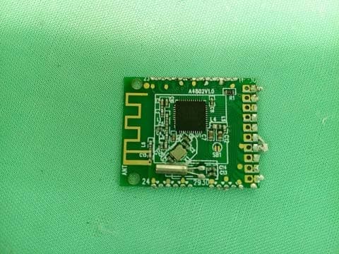
PEQA55000515
Jul 11, 2015Bluetooth Cooking Thermometer
Equipment Class
DTS - Digital Transmission System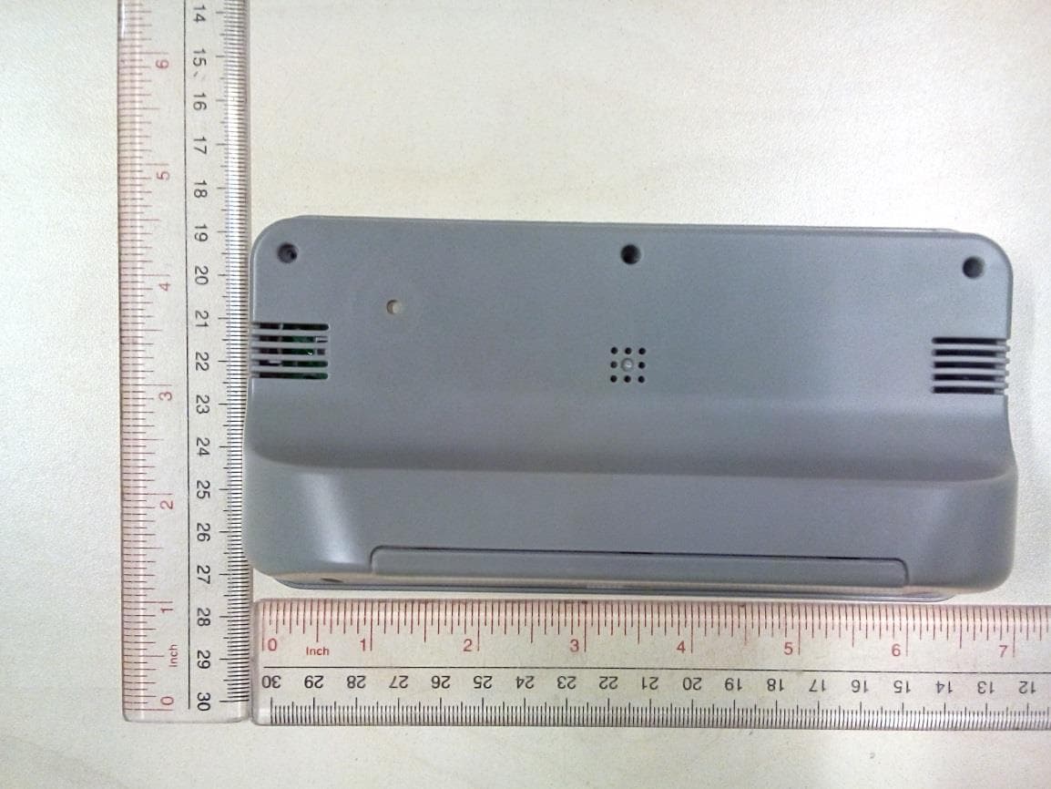
PEQ964F110813
Sep 16, 2014BLE Alarm Clock
Equipment Class
DTS - Digital Transmission System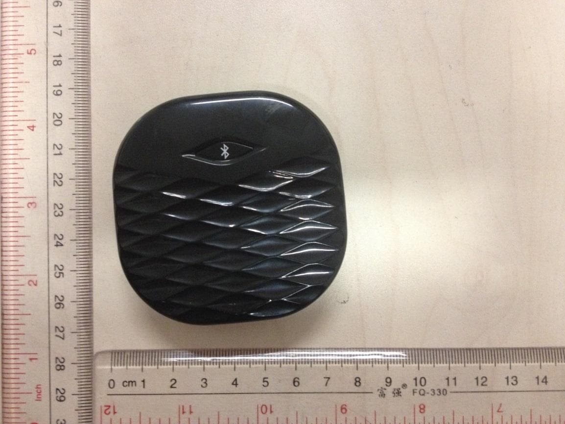
PEQA480110813
Sep 15, 2014BLE Vibration Alarm
Equipment Class
DTS - Digital Transmission System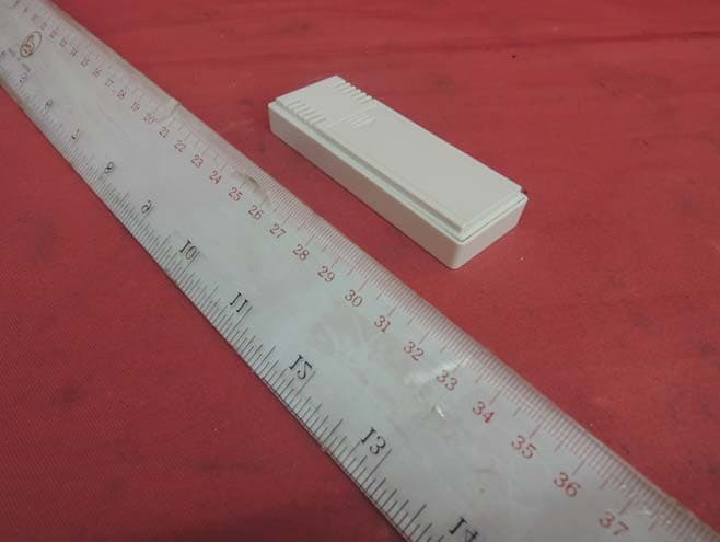
PEQA43071013
Oct 22, 2013Remote Thermo-Hygrometer
Equipment Class
DXX - Part 15 Low Power Communication Device Transmitter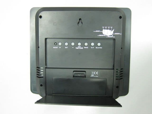
PEQ790E90712
Sep 02, 2012WWVB RC and RF wall clock
Equipment Class
CYY - Communications Receiver used w/Pt 15 Transmitter