PQRDS110-PCCWireless LAN card
Contec Co., Ltd.
Click to zoom
Application Details
- Equipment Class
- DSS - Part 15 Spread Spectrum Transmitter
- Date of Grant
- Sep 20, 2001
- Application Purpose
- Original Equipment
- Date of Application
- Sep 20, 2001
- Equipment Note
- Wireless LAN card
- Frequency Range
- 2411.93000000 - 2471.61000000
- Company
- Contec Co., Ltd.
- Country
- Japan
Documents & Files
Document Text
Text extracted from the exhibit documents filed with the FCC. Open a document above to read the original.
Users Manual
Introduction FX-DS110-PCC Precautions Related to Electromagnetic Interference This device complies with Part 15 of the FCC Rules. Operation is subject to the following two conditions : (1) this device may not cause harmful interference, and (2) this device must accept any interference received, including interference that may cause undesired operation. This equipment complies with part 15 of the FCC rules. Any changes or modifications not expressly approved by the manufacturer could void the user’s authority to operate the equipment. CAUTION: To comply with FCC RF exposure compliance requirements, a separation distance of at least 5 cm must be maintained between this device and all persons. Precautions Related to Service Clean the FX-DS110-PCC by wiping lightly with a soft cloth moistened with water or a cleaning solution. Take care to avoid the use of benzene, thinners or other volatile solutions which may cause deformation or discoloration. Notes! The unauthorized reproduction of this document, in whole or in part, is prohibited. The specifications, designs, and other contents of this document are subject to change without notice. The contents of this document are believed to be accurate, however if any discrepancies noted should be brought to the attention of the store where this product was purchased. Notwithstanding the foregoing, the manufacturer is unable to accept any claims for losses or lost profits, etc. Resulting from the use of this product. MS, Microsoft, Windows, Windows NT, and MS-DOS are registered trademarks or trademarks of Microsoft Corporation in the U.S.A. and other countries. Netscape Navigator is a registered trademark of Netscape Communications. Other names of companies and products used in this document trademarks or registered trademarks of the related companies. This document does not use the symbols ™ , ® , © etc.
Block Diagram
FX-DS110-PCC BLOCK DIAGRAM MAC Controller PC Card Interface Baseband Processor IF Modem RF Modem Power AMP LNA TX/RX Switch Antenna Switch Synthesizer VCO VCO
External Photos
External photo
ID Label/Location Info
Label format and Location Dimensions: 38 x 60mm 38mm 60mm Location The label is affixed to the rear side of main body.
Internal Photos
Internal photos
Operational Description
Technical Description of Unit Application of Use The equipment is a wireless LAN transmitter and receiver for use in an indoor environment. The equipment includes an integral antenna. Frequency range of operation 2412 to 2462 MHz (5 MHz interval, 11 waves) 25 mWEIRP Modulation CCK, QPSK or BPSK Chip rate 11 Mchips/s Data rate 11 Mbps Integral antenna Gain 2.14 dBi Other antennas None Determination and Stabilization of Frequency The equipment outputs 2412 to 2462 MHz (5MHz interval, 11 waves). The channel (frequency) is decided by a driver software. The frequency deviation is minimized to ±25 ppm or lower (at -10 to 70°C) by adapting synthesizer method in which the 44.0MHz crystal oscillator is used as a reference. The equipment includes regulator and supply electricity to each circuit shown below independently. The power to the PLL circuit is supplied separately in order to keep a constant supply voltage and for frequency stabilization. Modulation circuit PLL circuit RF mixture, amplifier circuit PLL circuit Crystal oscillator Frequency synthesizer Passive loop filter VCO circuit Attenuator Charge pump Frequency divider Phase Detection To M i x e r Frequency divider Suppression of spurious radiation Band-pass filters are installed in two stages to suppress the harmonics spurious radiation (2 x RF = 4824 to 4924 MHz, 3 x RF = 7236 to 7386 MHz and image spurious radiation caused by mixing (Lo - IF = 1664 to 1704 MHz). The attenuation at each frequency is shown in the lists below. Transmission circuit Specifications of band-pass filter (1) Item Specification Type MDR642E Manufacturer Soshin Electric Center frequency 2450 MHz 3dB band ±50 MHz Insertion loss 2.5 dB Max. Attenuation Lo - IF 1664 to 1714 MHz 50 dB or more Attenuation 2 x RF 4824 to 4924 MHz 35 dB or more Attenuation 3 x RF 7236 to 7386 MHz 30 dB or more Specifications of band-pass filter (2) Item Specification Type TDFM1B-2450T-10 Manufacturer Toko Center frequency 2450 MHz 3dB band ±50 MHz Insertion loss 2.0 dB Max. Attenuation Lo - IF 1664 to 1714 MHz 50 dB or more Attenuation 2 x RF 4824 to 4924 MHz 50 dB or more Attenuation 3 x RF 7236 to 7386 MHz 50 dB or more Lo = VCO oscillation frequency IF = IF frequency RF = RF frequency Mixer VCO Band-pass filter (1) Power amplifier Band-pass filter (2) Limiting Modulation The equipment includes base band processor HFA3861A which conducts the PSK (transmission rate 1, 2 Mbp) or CCK (transmission rate 5.5, 11 Mbp) modulation. The modulated signal is mixed with local oscillation signal at HFA3783 and be IF signal (374 MHz). The IF signal passes the SAW filter to suppress the 1st side lobe to -45 dBc. Specifications of SAW filter Item Specifications Type 855653 Manufacturer SAWTEK Center frequency 374 MHz 3dB band ± 8.5 MHz Insertion loss 11 dB Max. Attenuation 274 to 341 MHz 55 dB Typ Attenuation 341 to 352 MHz 60 dB Typ Attenuation 352 to 357.5 MHz 50 dB Typ Attenuation 390.5 to 396MHz 37 dB Typ Attenuation 396 to 430MHz 45 dB Typ Attenuation 430 to 474MHz 50 dB Typ Limiting power The equipment limits the power by keeping power supply voltage constant. The equipment is inserted into the PC card slot of personal computer or access point. The power supplied to the PC card slot should be 5V ± 5% according to the PC card standard. The equipment includes regulator and supplies electricity to each circuit shown below independently. Power limitation is carried out by supplying power independently to each circuit and keeping power supply voltage constant. Modulation circuit PLL circuit RF mixture, amplifier circuit Also the APC function is employed to keep the output voltage constant by comparing pre-set power value to detected power value. RF circuit 1) Modulation block The equipment performs PSK or CCK modulation/demodulation and spread/back spread spectrum by base band processor HFA3861A. The spread code used is 11 bit (transmission rate is 1, 2 Mbps) or 8 bittransmission rate is 5.5, 11 Mbps Code rate is 11 MChips/s. 2) Oscillation block The equipment has two VCO's which are controlled by the frequency synthesizer referencing to 44.0 MHz. Oscillation frequencies are 748 MHz and 2038 to 2088 MHz. 3) IF block The 748MHz oscillation signal is divided into two frequencies in the mixer HFA3783. Then it is mixed with modulation signal and be a 374MHz IF signal. The IF signal is amplified by the HFA3783 and then brought to the SAW filter (made by SAWTEK, model 855653, center frequency is 374MHz, and bandwidth is ± 8.5). HFA3783 also incorporates a receiving circuit. For receiving, modulation signal is selected from IF signals. During receiving, AGC circuit works to control gains according to the receiving power. 4) RF block The oscillation signal of 2038 to 2088 MHz is input to the mixer HFA3683 and mixed with IF signal to be RF signal. Then the RF signal passes band-pass filter to remove spurious emission and is amplified for about 27dB by power amplifier HFA3983. The amplified RF signal passes the transmitting/receiving switch, band-pass filter and antenna switching switch, and then is radiated to the air. The received RF signal passes antenna switching switch, band-pass filter and transmitting/receiving switch, and then is amplified by a low noise amplifier incorporated in HFA3683. The amplified signal is then mixed with 2038 to 2088 MHz signal to be IF signal.
RF Exposure Info
Prediction of MPE limit at a given distance Equation from page 18 of OET Bulletin 65, Edition 97-01 where:S = power density P = power input to the antenna G = power gain of the antenna in the direction of interest relative to an isotropic radiator R = distance to the center of radiation of the antenna Maximum peak output power at antenna input terminal:16.30 Maximum peak output power at antenna input terminal:42.65795(mW) Antenna gain(typical):2.14(dBi) Maximum antenna gain:1.636817(numeric) Prediction distance:5(cm) Prediction frequency:2400(MHz) MPE limit for uncontrolled exposure at prediction frequency:1(mW/cm^2) Power density at prediction frequency:0.222254(mW/cm^2) Maximum allowable antenna gain:8.671499(dBi) 2 4R PG S π =
Test Report
Nemko Test Report: 1L0472RUS1 Applicant: Contec Co. Ltd. 3-9-31 Himesato, Nishiyodogawa-ku Osaka 555-0025, Japan FCC ID# PQRDS110-PCC Equipment Under Test: FX-DS110-PCC (E.U.T.) In Accordance With: FCC Part 15, Subpart C, 15.247 Direct Sequence Spread Spectrum Transmitters Tested By: Nemko Dallas Inc. 802 N. Kealy Lewisville, Texas 75057-3136 Authorized By: Tom Tidwell, RF Group Manager Date: 7/31/01 Total Number of Pages: 45 Nemko Dallas FCC PART 15, SUBPART C DIRECT SEQUENCE SPREAD SPECTRUM TRANSMITTER EQUIPMENT: FX-DS110-PCC PROJECT NO.: 1L0472RUS1 Table of Contents Section 1. Summary of Test Results.......................................................................3 Section 2. Equipment Under Test (E.U.T.)............................................................5 Section 3. Powerline Conducted Emissions...........................................................8 Section 4. Minimum 6 dB Bandwidth..................................................................12 Section 5. Maximum Peak Output Power.............................................................16 Section 6. RF Exposure ........................................................................................17 Section 7. Spurious Emissions (conducted).........................................................18 Section 8. Spurious Emissions (radiated).............................................................22 Section 9. Peak Power Spectral Density...............................................................26 Section 10. Minimum Processing Gain................................................................30 Section 11. Test Equipment List...........................................................................31 ANNEX A - TEST DETAILS...............................................................................32 ANNEX B - TEST DIAGRAMS...........................................................................42 Page 2 of 45 Nemko Dallas FCC PART 15, SUBPART C DIRECT SEQUENCE SPREAD SPECTRUM TRANSMITTER EQUIPMENT: FX-DS110-PCC PROJECT NO.: 1L0472RUS1 Section 1. Summary of Test Results Manufacturer: Contec Co. Ltd. Model No.: FX-DS110-PCC Serial No.: None General: All measurements are traceable to national standards. These tests were conducted on a sample of the equipment for the purpose of demonstrating compliance with Part 15, Subpart C, Paragraph 15.247 for Direct Sequence Spread Spectrum devices. Radiated tests were conducted is accordance with ANSI C63.4-1992. Radiated emissions are made on an open area test site. A description of the test facility is on file with the FCC. New Submission Production Unit Class II Permissive Change Pre-Production Unit THIS TEST REPORT RELATES ONLY TO THE ITEM(S) TESTED. THE FOLLOWING DEVIATIONS FROM, ADDITIONS TO, OR EXCLUSIONS FROM THE TEST SPECIFICATIONS HAVE BEEN MADE. See “ Summary of Test Data”. NVLAP LAB CODE: 100426-0 Nemko Dallas Inc. authorizes the above named company to reproduce this report provided it is reproduced in its entirety and for use by the company’s employees only. Any use which a third party makes of this report, or any reliance on or decisions to be made based on it, are the responsibility of such third parties. Nemko Dallas Inc. accepts no responsibility for damages, if any, suffered by any third party as a result of decisions made or actions based on this report. This report applies only to the items tested. Page 3 of 45 Nemko Dallas FCC PART 15, SUBPART C DIRECT SEQUENCE SPREAD SPECTRUM TRANSMITTER EQUIPMENT: FX-DS110-PCC PROJECT NO.: 1L0472RUS1 Summary Of Test Data NAME OF TEST PARA. NO. SPEC. MEAS. RESUL T Powerline Conducted Emissions 15.207(a) 48 dBμV < 48 dBuV Complies Minimum 6 dB Bandwidth 15.247(a)(2) >500 kHz 10 MHz Complies Maximum Peak Power Output 15.247(b)(1) <1 Watt <1 Watt Complies Spurious Emissions (Antenna Conducted) 15.247(c) -20 dBc/100kHz < -20 dBc Complies Spurious Emissions (Restricted Bands) 15.247(c) < 74 dBuV/m Peak < 54 dBuV/m Avg < 74 dBuV/m Peak < 54 dBuV/m Avg Complies Peak Power Spectral Density 15.247(d) +8 dBm/3kHz < +8 dBm Complies Processing Gain 15.247(e) 10 dB > 10 dB Complies Footnotes: Page 4 of 45 Nemko Dallas FCC PART 15, SUBPART C DIRECT SEQUENCE SPREAD SPECTRUM TRANSMITTER EQUIPMENT: FX-DS110-PCC PROJECT NO.: 1L0472RUS1 Section 2. Equipment Under Test (E.U.T.) General Equipment Information Frequency Band: 902 – 928 MHz 2400 – 2483.5 MHz 5725 – 5850 MHz Tuning Range: 2411.93 - 2471.61 User Frequency Adjustment: Software controlled Page 5 of 45 Nemko Dallas FCC PART 15, SUBPART C DIRECT SEQUENCE SPREAD SPECTRUM TRANSMITTER EQUIPMENT: FX-DS110-PCC PROJECT NO.: 1L0472RUS1 Description of Modification for Modification Filing Family List Rational Page 6 of 45 Nemko Dallas FCC PART 15, SUBPART C DIRECT SEQUENCE SPREAD SPECTRUM TRANSMITTER EQUIPMENT: FX-DS110-PCC PROJECT NO.: 1L0472RUS1 Theory of Operation The equipment is a wireless LAN transmitter and receiver for use in an indoor environment. The equipment includes an integral antenna. System Diagram Page 7 of 45 Nemko Dallas FCC PART 15, SUBPART C DIRECT SEQUENCE SPREAD SPECTRUM TRANSMITTER EQUIPMENT: FX-DS110-PCC PROJECT NO.: 1L0472RUS1 Section 3. Powerline Conducted Emissions NAME OF TEST: Powerline Conducted Emissions PARA. NO.: 15.207(a) TESTED BY: David Light DATE:7/23/01 Test Results: Complies. Measurement Data: See attached plots. Measurement Uncertainty: +/- 1.7dB Page 8 of 45 Nemko Dallas FCC PART 15, SUBPART C DIRECT SEQUENCE SPREAD SPECTRUM TRANSMITTER EQUIPMENT: FX-DS110-PCC PROJECT NO.: 1L0472RUS1 Test Data – Powerline Conducted Emissions Page 9 of 45 Nemko Dallas FCC PART 15, SUBPART C DIRECT SEQUENCE SPREAD SPECTRUM TRANSMITTER EQUIPMENT: FX-DS110-PCC PROJECT NO.: 1L0472RUS1 Test Data – Powerline Conducted Emissions Test Data – Powerline Conducted Emissions Nemko Dallas FCC PART 15, SUBPART C DIRECT SEQUENCE SPREAD SPECTRUM TRANSMITTER EQUIPMENT: FX-DS110-PCC PROJECT NO.: 1L0472RUS1 Page 10 of 45 Page 10 of 45 Nemko Dallas FCC PART 15, SUBPAR…
Text truncated - open the document above for the full version.
Test Report
HFA3861A Data Rate Symbol Rate Chip Rate 1 Mbps 1 Msps 11 Mcps 2 Mbps 1 Msps 11 Mcps 5.5 Mbps 1.375 Msps 11 Mcps 11 Mbps 1.375 Msps 11 Mcps The HFA3861 transmitter is a Direct Sequence Spread Spectrum Phase Shift Keying (DSSS PSK) modulator. It can handle data rates of up to 11Mbps. The various modes of the modulator are: Modulation Data Rate DBPSK 1 Mbps DQPSK 2 Mbps CCK 5.5 Mbps CCK 11 Mbps These implement data rates as shown in Table 3. The major functional blocks of the transmitter include a network processor interface, DPSK modulator, high rate modulator, a data scrambler and a spreader, as shown in Figure 7. CCK is essentially a quadra- phase form of M-ARY Orthogonal Keying. A description of that modulation can be found in Chapter 5 of: “Telecommunications System Engineering”, by Lindsey and Simon, Prentis Hall publishing. The preamble is always transmitted as the DBPSK waveform while the header can be configured to be either DBPSK, or DQPSK, and data packets can be configured for DBPSK, DQPSK, or CCK. The preamble is used by the receiver to achieve initial PN synchronization while the header includes the necessary data fields of the communications protocol to establish the physical layer link. The transmitter generates the synchronization preamble and header and knows when to make the DBPSK to DQPSK or CCK switchover, as required. The classical definition of processing gain is the 10 Log number [rC/rB] in dB. By this definition a system that has a data rate of 1MBPS and a chip rate (rate of PN code) of 1MCPS will have a PG of 10.41dB. Using the PRISM chip set each data bit is x-ored with an 11 bit sequence for this particular example. The processing gain can be then viewed as the 10Log[11]dB where 11 is the length of the PN code. If a code with a length of 16 bits is to be used then the processing gain is equivalent to 10 Log[16] dB or 12.04dB. Data Demodulation in the CCK Modes In this mode, the demodulator uses Complementary Code Keying (CCK) modulation for the two highest data rates. It is slaved to the low rate processor which it depends on for acquisition of initial timing and phase tracking information. The low rate section acquires the signal, locks up symbol and carrier tracking loops, and determines the data rate to be used for the MPDU data. The demodulator for the CCK modes takes over when the preamble and header have been acquired and processed. On the last bit of the header, the phase of the signal is captured and used as a phase reference for the high rate differential demodulator. Control of the demodulator is then passed to the high rate section. The signal from the A/D converters is carrier frequency and phase corrected by a complex multiplier (mixer) that multiplies the received signal with the output of the Numerically Controlled Oscillator (NCO) and SIN/COS look up table. This removes the frequency offset and aligns the I and Q Channels properly for the correlators. The sample rate is decimated to 11MSPS for the correlators after the complex multiplier since the data is now synchronous in time. The Fast Walsh transform correlation section processes the I and Q channel information. The demodulator knows the symbol timing, so the correlation is batch processed over each symbol. The correlation outputs from the correlator are compared to each other in a biggest picker and the chosen one determines 6 bits of the symbol. The QPSK phase of the chosen one determines two more bits for a total of 8 bits per symbol. Six bits come from which of the 64 correlators had the largest output and the last two are determined from the QPSK differential demod of that output. In the 5.5Mbps mode, only 4 of the correlator outputs are monitored. This demodulates 2 bits for which of 4 correlators had the largest output and 2 more for the QPSK demodulation of that output for a total of 4 bits per symbol. ChannelData RateProcessing Gain (dB) 11Mbps13.3 12Mbps13.1 111Mbps14.1 61Mbps13.4 62Mbps12.9 611Mbps13.9 111Mbps13.2 112Mbps13.1 1111Mbps13.8 Data RateS/Nout(dB)PER% Method Of Measurement: The CW jamming margin method was used to determine the processing gain. A CW signal generator is stepped across the passband of the receiver in 50 kHz increments. At each point the signal generator level required to obtain the recommended bit error rate is recorded. The jammer to signal ratio (J/S) is then calculated. The worst 20% of the J/S points is discarded. The lowest remaining J/S ratio is used to calculate the processing gain. Calculation Of Processing Gain: The processing gain was determined by measuring the jamming margin of the E.U.T. and using the following formula: Jamming Margin = G p - (S/N) out - L sys For a receiver using non-coherent detection the value (S/N) out is calculated using the formula: P e = (1/2)EXP{-E/2N o } where P e is the probability of error (minimum Bit Error Rate required for proper operation). E/N o is (S/N) out for example, for a bit error rate of 10 -4 a S/N ratio of 12.3 dB is required. L sys (system losses) is assumed to be 2 dB. Therefore G p = Mj + (S/N) out + L sys 1 Mbps10.3<=8.0 2 Mbps13.3<=8.0 11 Mbps16.4<=8.0 Processing Gain ISL37400M 2Mbps CHANNEL 1 Processing Gain Gp = (S/N)o + Mj + Lsys Freq.Gp(S/N)oMj=J/SLsysJammerPER (MHz)(dB)(dB)(dB)(dB)(dBm)(%) 2403.5023.013.37.72.0-52.3<=8.0 2403.5522.213.36.92.0-53.1<=8.0 2403.6021.413.36.12.0-53.9<=8.0 2403.6520.613.35.32.0-54.7<=8.0 2403.7020.313.35.02.0-55.0<=8.0 2403.7520.513.35.22.0-54.8<=8.0 2403.8019.813.34.52.0-55.5<=8.0 2403.8519.813.34.52.0-55.5<=8.0 2403.9019.713.34.42.0-55.6<=8.0 2403.9520.113.34.82.0-55.2<=8.0 2404.0019.413.34.12.0-55.9<=8.0 2404.0519.613.34.32.0-55.7<=8.0 2404.1018.913.33.62.0-56.4<=8.0 2404.1520.013.34.72.0-55.3<=8.0 2404.2020.613.35.32.0-54.7<=8.0 2404.2520.813.35.52.0-54.5<=8.0 2404.3020.613.35.32.0-54.7<=8.0 2404.3520.913.35.62.0-54.4<=8.0 2404.4020.913.35.62.0-54.4<=8.0 2404.4520.313.35.02.0-55.0<=8.0 2404.5019.813.34.52.0-55.5<=8.0 2404.5519.513.34.22.0-55.8<=8.0 2404.6020.21…
Text truncated - open the document above for the full version.
Test Setup Photos
Test setup photos
Contact Information
Applicant
Mr. Naoki Ikeda(Approval Contact)
Test Firm
Nemko Dallas, Inc.Michael Cantwell
Technical Specifications
| # | Rule Parts | Frequency Range | Power Output |
|---|---|---|---|
| 1 | 15C | 2.41 GHz - 2.47 GHz | 43.00 mW |
Other Applications from Contec Co., Ltd.

PQRFXE2000-DG
Apr 08, 2014Wireless LAN Adapter
Equipment Class
NII - Unlicensed National Information Infrastructure TX
PQRFXA2000-G
Jan 13, 2013IEEE802.11n/a/b/g Wireless LAN (Access Point/Station)
Equipment Class
DTS - Digital Transmission System
PQRFXE2000-G
May 28, 2012Wireless LAN Adapter
Equipment Class
DTS - Digital Transmission System
PQRNZ2WL-US
Apr 24, 2011Wireless LAN Adapter
Equipment Class
NII - Unlicensed National Information Infrastructure TX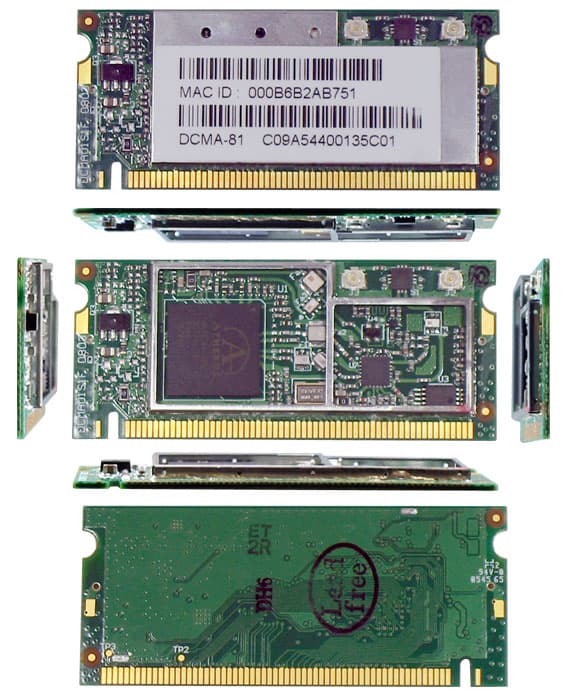
PQRDS540-MPCI6
Mar 28, 2006Wireless LAN MiniPCI Card
Equipment Class
NII - Unlicensed National Information Infrastructure TX