QFENTP6348S2.4GHz Cordless Telephone W Call Waiting Caller ID
Newcont Electronic Co., Ltd.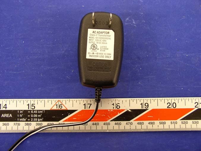
Click to zoom
Application Details
- Equipment Class
- DXX - Part 15 Low Power Communication Device Transmitter
- Date of Grant
- Feb 26, 2004
- Application Purpose
- Original Equipment
- Date of Application
- Feb 26, 2004
- Equipment Note
- 2.4GHz Cordless Telephone W Call Waiting Caller ID
- Frequency Range
- 2472.00000000 - 2475.90000000
- Company
- Newcont Electronic Co., Ltd.
- Country
- China
Documents & Files
Document Text
Text extracted from the exhibit documents filed with the FCC. Open a document above to read the original.
Block Diagram
RX DATA APPROVALCHECKPREPARE Model 6348 Base Block Diagram RF Module Expander Data Comparator CPU Tele Speech Tel Jack Carrier Detcct RX Power Control Compressor Audio Input TX DATA Reset Circurt Line Detect Charge Detect Audio Output Line Control FSK 5V DC 5V 5V PLL Data TX Power Control RX DATA APPROVALCHECKPREPARE Model 6348 Hand Block Diagram RF Module Expander Data Compartor CPU Carrier Detect RX Power Control PLL Data TX Power Control Compressor Audio Input Reset key Audio Output Amp output SP mic LCD Display Battery Low Detect Charge Detect TX DATA 3.8V Battery APPROVALCHECKPREPARE Model 6348 Base RF Module Block Diagram RF Receiver BPF 2473.000MHz±3MHz RF Transmitter BPF 2404.000MHz±3MHz Ant 2472.000~2475.900M Hz LNA Pre- AMP 450KHz Mix2 IF1BPF LIM AMP DEM Audio Output Carrier Detect 2482.700~2486.600MHz/ 3RX-VCO Dual Frequency Synthesizer 2403.050~2406.950MH z PA 2403.050~2406.950MHz /3 TX-VCO MOD Audio Input ×3 ×3 PLL DATA 10.7MHz Mix1 11.150MHz TX Power RX Power APPROVALCHECKPREPARE Hand RF Module Block Diagram Model 6348 RF Receiver BPF 2404.000MHz±3MHz RF Transmitter BPF 2473.000MHz±3MHz Ant 2403.050~2406.950M HzLNA Pre- AMP 450KHz Mix2 IF1BPF LIM AMP DEM Audio Output Carrier Detect 2392.350~2396.250MHz /3 RX-VCO Dual Frequency Synthesizer 2472.000~2475.900MH z PA 2472.000~2475.900MHz /3TX-VCO MOD Audio Input Detector ×3 ×3 PLL DATA 10.7MHz Mix1 11.150MHz TX Power Rx Power
External Photos
NEWCONT ELE CO., LTD. FCC ID: QFENTP6348S Power Supply –Top View Power Supply –Bottom View NEWCONT ELE CO., LTD. FCC ID: QFENTP6348S Power Supply –Side View
External Photos
NEWCONT ELE CO., LTD. FCC ID: QFENTP6348S EXHIBIT C - EUT PHOTOGRAPHS EUT – Over View EUT – Port View NEWCONT ELE CO., LTD. FCC ID: QFENTP6348S Chassis –Front View Chassis –Rear View NEWCONT ELE CO., LTD. FCC ID: QFENTP6348S Base –Rear View
External Photos
NEWCONT ELE CO., LTD. FCC ID: QFENTP6348S Handset –Front View Handset –Rear View NEWCONT ELE CO., LTD. FCC ID: QFENTP6348S Handset –Bottom View
ID Label/Location Info
EXHIBIT A - FCC ID LABEL INFORMATION Proposed FCC ID Label Specifications : Text is black or white in color and is left justified. Labels are silk-screened and shall be “permanently affixed” at a conspicuous location on the EUT. Proposed Label Location on EUT FCC ID Label FCC ID: QFENTP6348S This device complies with Part 15 o the FCC Rules. Operation is subject to the following two conditions: (1) this device may not cause harmful interference, and (2) this device must accept any interference received, including interference that may cause undesired operation. 2.1875" 1.0" FCC IDL: I38NA3800 This device complies with Part 15 o the FCC Rules. Operation is subject to the following two conditions: (1) this device may not cause harmful interference, and (2) this device must accept any interference received, including interference that may cause undesired operation. 2.1875" 1.0" FCC IDL: I38NA3800 This device complies with Part 15 o the FCC Rules. Operation is subject to the following two conditions: (1) this device may not cause harmful interference, and (2) this device must accept any interference received, including interference that may cause undesired operation. 2.1875" 1.0"
Internal Photos
NEWCONT ELE CO., LTD. FCC ID: QFENTP6348S Chassis –Cover off View Base – Component View NEWCONT ELE CO., LTD. FCC ID: QFENTP6348S Base – Solder View Base – Transceiver & Antenna Top View NEWCONT ELE CO., LTD. FCC ID: QFENTP6348S Base – Transceiver & Antenna Bottom View Base – Transceiver & Antenna Component View NEWCONT ELE CO., LTD. FCC ID: QFENTP6348S Base – Transceiver & Antenna Solder View Base – PCB I Component View (1) NEWCONT ELE CO., LTD. FCC ID: QFENTP6348S Base – PCB I Component View (2) Base – PCB I Solder View NEWCONT ELE CO., LTD. FCC ID: QFENTP6348S Base – PCB II Component View Base – PCB II Solder View NEWCONT ELE CO., LTD. FCC ID: QFENTP6348S Base – Page & Led PCB Component View Base –Page & Led PCB Solder View
Internal Photos
NEWCONT ELE CO., LTD. FCC ID: QFENTP6348S Handset –Cover off View Handset –Component View NEWCONT ELE CO., LTD. FCC ID: QFENTP6348S Handset –Solder View Handset –PCB View (1) NEWCONT ELE CO., LTD. FCC ID: QFENTP6348S Handset –PCB View (2) Handset –PCB View (3) NEWCONT ELE CO., LTD. FCC ID: QFENTP6348S Handset –PCB View (4) Handset –PCB View (5) NEWCONT ELE CO., LTD. FCC ID: QFENTP6348S Handset –PCB View (6)
Operational Description
6348 CIRCUIT DESCRIPTION 1 Base a. RF Transmitter Section – RF Board The compressed audio signal (RF module pin 10) is modulated through the varactor diode VD201. These components, i.e. VD201, C216, L201, Q5 and the external components of Q5 compose the voltage controlled oscillator circuit for the transmitter part. This circuit generates the TX VCO frequency. A portion of this signal is fed back to the PLL IC (LMX1602)’s pin12 (FIN1) for phase comparison. Once the phase of oscillation stabilized, the PLL circuit generates the error voltage necessary for the VCO to oscillate at the desired transmitter’s RF frequency. The VCO circuit impedance is matched with the succeeding circuit through the transistor Q202 that also acts as the buffer amplifier. The RF amplifier Q201 boosts the signal for transmission. This amplified RF signal is trimmed to the desired frequency band by F2 (BPF2403) so as not to interfere with the receiver circuit. The transmitter RF signal is then propagated through the antenna. b. RF Receiver Section – RF Board The Base Unit antenna receives RF signal. The Band Pass Filter F1 (BPF2475) trims the signal to the desirable frequency band. Transistor Q101 $ Q104 is a low noise amplifier that boosts the RF signal to a specific level for mixing. PLL U2 (LMX1602) is used as a Universal Phase Lock Loop circuit. The frequency from the Voltage Controlled Oscillator (VCO) VD101, L102 and Q103, is fed back to the PLL IC through pin 5 (FIN2) for phase comparison. During channel scanning or turning the unit on, once the phase of oscillation stabilized (locked), the PLL circuit generates the first local oscillator frequency for down-converting the received RF signal into the first IF frequency 10.7Mhz. This process is accomplished through the IF mixer circuit Q104. Q104 is used for matching the impedance of the mixer circuit with the succeeding circuits. The resulting IF signal is kept constant by the IF Filter F3 to 10.7MHz which is then mixed with the second local oscillator frequency 11.150MHz (derived from X1 & VC1) to produced a much lower IF frequency. This lower IF frequency if further filtered by IF Filter FL4 to produce a more stable signal of 450KHz. Quadrature signal detection is accomplished internally by the Narrow-band Detector IC2 (KA3361) with the IF coil T1. The recovered audio frequency can be taken from U1 audio output pin9. c. Transmitter Audio Section – Main Board The Audio Frequency signal from the telephone line that is through Q2, R4, R9, R58, C36, etc is compressed through the compressor part of IC2 to minimize the transmission noise. The degree of compression depends on the external RC combinations. AGC is also utilized by IC2 to avoid shock noise caused by abrupt change of audio levels. The compressed audio is filtered and amplified for better acoustical performance. d. Receiver Audio Section – Main Board The compressed Audio Frequency signal from the RF module (pin3) is passed through passive RC filters for acoustic compliance. The filtered audio is then fed to the Compander IC2 (pin16 and pin17) for expansion thus retrieving the original Audio signal with noise filtered out. Q1 is used as buffer circuit. Bridge rectifier D1,D2,D6,D7 isolates the high-voltage telephone line to the rest of the circuit. 2 Handset a. RF Transmitter Section – RF Board Refer to portion 1.b for this section. All circuit performance is the same except that Band Pass Filter BPF2403 is changed to BPF2475 for the handset transmission. b. RF Receiver Section – RF Board Refer to portion 1.b for this section. All circuit performance is the same except that Band Pass Filter BPF2475 is changed to BPF2403 for the handset transmission. c. Transmitter Audio Section – Main Board Audio Frequency signal from the handset or from the headset microphone is compressed through the compressor part of IC3 to minimize the transmission noise. The degree of compression depends on the external RC combinations. AGC is also utilized by IC3 to avoid shock noise caused by abrupt change of audio levels. The compressed audio is filtered and amplified for better acoustical performance. Q9 is a switching transistor that controls the power supply for the TX RF part. d. Receiver Audio Section – Main Board The compressed Audio Frequency signal from the RF module is passed through passive RC filters for acoustic compliance. The filtered audio is then fed to the Compander IC3 for expansion thus retrieving the original audio signal with noise filtered out. Q1 & Q4 act as audio amplifier to sufficiently drive the handset speaker. Q5 and Q6 are switching transistors that control the power supply for the RF part, the Compander part and the AF amplifier respectively. An earphone jack is provided for an optional headset unit for hands free conversation on the handset. 3 OTHERS (Handset): a. Charging and Reset Controls Recharging the handset battery is accomplished by putting the handset on the cradle. Q8 and its external components are the reset circuit. R55 and R56 detect this action and send a command to the CPU (IC1 pin24) for proper exchange of security code. b. Ring Detection When the handset receives the ring command from the base unit, the CPU will send buzzer signal to the ringer amplifier Q2 and Q3 that drives the Buzzer. 4 OTHERS (Base): a. Hook Switching and Dialing The transistor Q4 that is controlled by the IC1 (pin21) accomplishes the hook switching and the pulse dialing function. The DTMF signal from the IC1(pin29) is amplified by Q8. b. Over-voltage Protection Fuse 1 and varistor ZR1 act as high current and high voltage protectors for the telephone line interface. In case of presence of voltage surge across the telephone line, Fuse 1 decreases its resistance and dumps the line voltage to a safe level. Fuse1 opens when excessive current is present on the line thus protecting both the user and the line interface. c. Battery Charging & Code Setting Battery charging commences when Q6 detects the presence of th…
Text truncated - open the document above for the full version.
Operational Description
(MHz) 2.4GHz Frequency Table with Span 100KHz
Operational Description
NEWCONT ELECTRONICS LTD ISSUED DATE :14-Jan-04 MODEL: 6348 1. Standard Voltage: Handset unit DC 3. 8 V +/- 0.1 V Base unit AC 110 V +/- 10% V DC 9V 300 mA 2. Temperature: 25 °C +/-5 °C 3. Bell Signal Frequency: 25 Hz ( 70 VR.M. S.) 4. Frequency: B/U TX Frequency 2403.0502406.950 H/S TX Frequency 2472.0002475.900 5. Modulation mode: FM HANDSET P0WER CONSUMPTION: DESCRIPTION Units Nominal Limit A) TALK mode Current 3.8V POWER mA 80 88 B) STAND-BY mode 3.8V POWER Current.( AVG) mA 3.5 < 4.0 D) Battery Low V 3. 3 ± 0.15 BASE UNITS 1) POWER CONSUMPTION: DESCRIPTION Units Nominal Limit A) TALK mode (DC 9V) mA 100 <150 B) Stand-By mode (DC 9V) mA 40 < 60 C) Charge Current to 3.6v Battery mA 50 ± 10 2) RINGER STATE: DESCRIPTION Units Nominal Limit HI VOL dB 73 > 70 D ) Ringer level ( 50CM ) LO VOL. dB 66 > 63 NEWCONT ELECTRONICS LTD 3) TELEPHONE SIGNAL(DTMF/TONE/ PULSE/FLASH): DESCRIPTION Units Nominal Limit A) DTMF Frequency Error % 1 ± 1.3 B) DTM FLEVEL LOW Group HIGH Group dBm. -7 -5 ± 2.8 ± 2.8 C) Pre-Emphasis (Twist) dB 2.0 0~4.0 D) Pulse M/B ratio % 40 38 ~ 42 E) Pusle rate PPS 10 ± 1 F) Flash time mS 600 ± 50 4) OTHER-FUNCTIONS: DESCRIPTION Units Nominal Limit A) Security Code 65536 B) Clear Down 450M C) Acoustic Line (600Ù) SLR 0Kft RLR STMR dB -46 46 10 -45 ~ -48 44 ~ 48 > 5 SLR 9Kft RLR STMR dB - 42 48 10 -40 ~ -44 46 ~ 50 > 5 SLR 15Kft RLR STMR dB -38 51 10 -36 ~ -42 50 ~ 54 > 5 D) Receive Volume Difference dB 13 12-16 E) Receive & sending Distortion % 3 5 F) Return loss dB 16 G) Earphone Receive Volume Difference dB 9 8 ~ 12 H) Earphone Receive Volume level dB 41 ± 2 I) Receive & sending responses Fail/pass Pass Confirm 5) SAFETY DESCRIPTION Units Nominal Limit A) Electrical & Insulation Strength AC Test Voltage 1.0 mA 3 Second KV 1.2 No Breakdown 6) CALL ID : DESCRIPTION Units Nominal A) FSK Detector level 15dB S/N dBm -2~ -42 B) Call ID Detector level dBm -2~ -38 C) Call Waiting Detector level dBm -2~ -38
Parts List/Tune Up Info
NO SERIAL NO COMPONENTS MODEL RATINGS QTY LOCATION BASE UNIT I B/SPCB 1 B/S PCB SMD MATERIAL 1 2648500020 CIRCUIT BOARD NTP4850BM030930 B/S BOARD 1 PCB 2 1510000210 SMD RES 0 Ω 0603/±5% 2 R58 R57 3 1511001210 SMD RES 100 Ω 0603/±5% 1 R56 4 1512201210 SMD RES 220 Ω 0603/±5% 2 R7,R11 5 1514701210 SMD RES 470 Ω 0603/±5% 1 R10 6 1516801210 SMD RES 680 Ω 0603/±5% 1 R8 7 1518201210 SMD RES 820 Ω 0603/±5% 1 R5 8 1513302210 SMD RES 3.3K Ω 0603/±5% 2 R9,R22 9 1516802210 SMD RES 6.8 K Ω 0603/±5% 2 R2,R4 10 1514702210 SMD RES 4.7K Ω 0603/±5% 1 R51 11 1511003210 SMD RES 10K Ω 0603/±5% 6 R13,R18,R32,R34,R44,R3 12 1511503210 SMD RES 15K Ω 0603/±5% 2 R6,R1 13 1513303210 SMD RES 33K Ω 0603/±5% 2 R50,R52 14 1514703210 SMD RES 47K Ω 0603/±5% 6 R12,R21,R29,R36,R48,R49 15 1511004210 SMD RES 100K Ω 0603/±5% 10 R16,R23,R28,R33,R37,R38,R39,R42,R43,R47 16 1511504210 SMD RE 150 K Ω 0603/±5% 1 R30 17 1512204210 SMD RES 220K Ω 0603/±5% 2 R171,R59 18 1513304210 SMD RES 330K Ω 0603/±5% 2 R45,R46 19 1514704210 SMD RES 470K Ω 0603/±5% 1 R31 20 1511005210 SMD RES 1M Ω 0603/±5% 1 R35 21 1512205210 SMD RES 2.2M Ω 0603/±5% 1 R19 22 1512206210 SMD RES 22M Ω 0603/±5% 2 R40,R41 23 1442704341 OC SMD CAP 27PF 25V/0603/±5% NPO 2 C4,C5 24 1442215341 OC SMD CAP 22 0PF 25V/0603/±10% NPO 1 C1A 25 1443915341 OC SMD CAP 390PF 25V/0603/±10% NPO 1 C14 26 1441026341 OC SMD CAP 1NF 25V/0603/±20% Y5V 1 C25 27 1444726341 OC SMD CAP 4.7 NF 25V/0603/±20% Y5V 1 R20 28 1441036041 OC SMD CAP 10NF 25V/0603/±20% Y5V 9 C2,C11,C13,C24,C26,C27,C28,C6,C3 29 1441536041 OC SMD CAP 15NF 25V/0603/±20% Y5V 1 C1 DESIGN ENGINEER WORKSHOP ENGINEER 3/1/2004 400004 1 18 DESIGN ENGINEER WORKSHOP ENGINEER 30 1444736041 OC SMD CAP 47NF 25V/0603/±20% Y5V 1 C12 31 1441046041 OC SMD CAP 100NF 25V/0603/±20% Y5V 6 C7,C8,C16,C21,C22,C23 32 1209014400 SMD TRANSISTOR MMBT9014C 200< β <350 SOT-23 NPN 2 Q5,Q6 33 1208050400 SMD TRANSISTOR S8050H (J3Y) 200< β <350 SOT-23 NPN 1 Q8 2 B/S PCB INJECTION PARTS 1 JUMP WIRE 6mm 15 J1,J2A,J3,J4,J5,J6,J7,J8 J9,J15,J16,J17,J18,J19,J20 2 JUMP WIRE 10mm 4 J10,J11,J12,J13 3 JUMP WIRE 15mm 1 J14 4 1501000250 LEAD TYPE RES 10 Ω 1/4W/±5% 1 R15 5 1501800250 LEAD TYPE RES 18 Ω 1/4W/±5% 1 R14 6 1507500250 LEAD TYPE RES 75 Ω 1/4W/±5% 1 R53 7 1501004250 LEAD TYPE RES 100K Ω 1/4W/±5% 2 R24,R25 8 1501802240 LEAD TYPE RES 1.8K Ω 1/8W/±5% 2 R26,R27 9 14310260B0 HIGH-VOLTAGE CER A 102 1KV/±20% 5 C9,C10,C19,C20,C25 10 14310360B0 HIGH-VOLTAGE CER A 103 1KV/±20% 2 C15,C17 11 1422245090 LEAD TYPE TERYLENE CAP 224(FOOT DISTANCE)10mm 250V/±10% LENGTH 12×5.3×10.8mm 1 C18 12 1402266030 AL EL CAP 22 uF 16V/±20% Φ 5×11 1 E2 13 1401076030 AL EL CAP 100μF 16V/±20% Φ 5×11 1 E1 14 1404776040 AL EL CAP 470μF 25V/±20% Φ 8×14 3 E5,E4,E3 15 1301500010 ZENER DIODE 15V 0.5W 2 DW1, DW2 16 2720000010 SURGE PROTECTOR STPA200 1 ZR1 17 1314004010 ZENER DIODE IN4004 8 D1,D2,D3,D4,D5,D6,D7,D11 18 1314148010 ZENER DIODE 1N4148 5 D8,D9,D10,D12,D13 19 2011001210 INDUCTOR 10μH ±10% EC36 0307 6 L1,L3,L4,L5 L6,L2 20 2325003510 FUSE 350mA 250V WITH FOOT 3CM( Ф 4×11.5) walter 1 FUSE1 21 1703580310 CRYSTAL 3.58MHz 20PPM 20PF 1 JT1 22 1208050610 ZENER TRANSISTOR S8050D 200< β <350 TO-92 NPN 1 Q1 23 1219200610 ZENER TRANSISTOR KSP92 80< β <160 TO-92 PNP 2 Q2,Q3 24 1204200610 ZENER TRANSISTOR KSP42 80< β <160 TO-92 NPN 1 Q4 25 11678050A1 OC LEAD TYPE IC LM7805 1 IC3 3 B/S PCB WELDING PARTS 1 2500000000 DC-JACK DC-470 1 JK2 3/1/2004 400004 2 18 DESIGN ENGINEER WORKSHOP ENGINEER 2 2502000100 BAT-JACK 623PCB (DOUBLE JACK) BLACK 1 JK1 3 2140000220 SLIDE SWITCH SS—12D25-G5 HANDLE LENGTH 5mm 1K1 4 2521140400 FLAT CABLE 3+40+3mm×14PIN×2.0mm 1 B/S BOARD TO BMS BOARD 5 1133240140 OC SMD IC LM324M SOP 1 IC2 6 2150000010 TOUCH SWITCH 6×6×4.3 1 PAGE1 7 1350121020 DIODE Φ 2mm RED COLOR FLAT HEAD 1 LED1 8 1350301010 ZENER DIODE Φ 3mm WHITE WITH RED COLOR (LONG FOOT 27mm) 1 LED2 II B/S BONDING PARTS 1 2638500210 CIRCUIT BOARD TCC150MCU-3850 030308 B/S BONDING 1 CPU BONDING BOARD 2 1110160000 BONDING IC S3P7588XZZ OTP 1 1 B/S BMS PCB SMD PARTS 1 2648150010 CIRCUIT BOARD NTP4815BMS030620 B/S BOARD 1 PCB 2 1511001210 SMD RES 100 Ω 0603/±5% 1 R63 3 1511002210 SMD RES 1K Ω 0603/±5% 1 R57 4 1514702210 SMD RES 4.7K Ω 0603/±5% 2 R61,R0 5 1511003210 SMD RES 10K Ω 0603/±5% 6 R24/9,R58,R64,R71,R72,R70 6 1511503210 SMD RES 15K Ω 0603/±5% 1 R68 7 1512203210 SMD RES 22K Ω 0603/±5% 1 R67 8 1513303210 SMD RES 33K Ω 0603/±5% 1 R66 9 1513903210 SMD RES 39K Ω 0603/±5% 1 R74 10 1514703210 SMD RES 47K Ω 0603/±5% 3 R56,R62,R75 11 1515603210 SMD RES 56K Ω 0603/±5% 2 R69,R65 12 1511804210 SMD RES 18 0K Ω 0603/±5% 1 R59 13 1514704210 SMD RES 470K Ω 0603/±5% 1 R60 14 1518204210 SMD RES 820K Ω 0603/±5% 2 R54,R55 15 1444715341 OC SMD CAP 470PF 25V/0603/±10% NPO 1 C41 16 1446815341 OC SMD CAP 680P 25V/0603/±10% Y5V 2 C38,C39 17 1444726341 OC SMD CAP 4.7NF 25V/0603/±20% Y5V 1 C34 18 1441036041 OC SMD CAP 10NF 25V/0603/±20% Y5V 3 C28,C29,C40 19 1441536041 OC SMD CAP 15 NF 25V/0603/±20% Y5V 1 C33 20 1441046041 OC SMD CAP 100NF 25V/0603/±20% Y5V 6 C30,C31,C32,C35,C36,C37 21 1218550400 SMD TRANSISTOR S8550LT1(2TY) 120< β <200 SOT-23 PNP 1 Q7 II B/S BMS PCB 3/1/2004 400004 3 18 DESIGN ENGINEER WORKSHOP ENGINEER 22 1209014400 SMD TRANSISTOR MMBT9014C 200< β <350 SOT-23 NPN 1 Q8 2 B/S BMS PCB INJECTION PARTS JUMP WIRE 6mm 4 J27,J28,J30,J22 JUMP WIRE 10mm 6 J21,J23,J24,J25,J26,J29 1 1404746050 AL EL CAP 0.47μF 50V/±20% Φ 5×11 1 E9 2 1401056050 AL EL CAP 1μF 50V/±20% Φ 5×11 2 E7,E11 3 1401066050 AL EL CAP 10μF 50V/±20% Φ 5×11 2 E6,E12 4 1401076030 AL EL CAP 100μ 16V/±20% Φ 5×11 3 E8,E10,E13 5 1545003110 LEAD ADJUSTABLE R 50K Ω 2 VR1,VR2 3 B/S BMS PCB WELDING PARTS 1 2521100300 FLAT CABLE 3+30+3mm×10PIN×2.0mm 1 2 RFB2403A20 Z HIGH VOLTAGE MOD U 2.4GHzRF(B/S) 1 3 1138507040 OC SMD IC KA8507BD SOP 1 IC4 5 1511004210 SMD RES 100K Ω 0603/±5% 1 B/S ASSEMBLING PARTS 1 ASSEMBLING ELECTRONICS PARTS 1 2520080900 WIRE 90mm(BLACK) Φ 0.8mm 1 LED- 2 2520080902 WIRE 90mm(RED) Φ 0.8mm 1 LED+ 3 2520081200 WIRE 120mm(BLACK) …
Text truncated - open the document above for the full version.
Schematics
2400BRFB.SCH-1 - Fri Feb 06 15:24:59 2004
Schematics
2400BRFH.SCH-1 - Fri Feb 06 15:35:32 2004
Test Report
Note: This test report is specially limited to the above client company and the product model only. It may not be duplicated without prior written consent of Bay Area Compliance Laboratory Corporation. This report must not be used by the client to claim product endorsement by NVLAP or any agency of the U.S. Government. FCC PART 15 Subpart C EMI MEASUREMENT AND TEST REPORT For NEWCONT ELE CO., LTD. 40F, BLOCK C SCIENCE & TECHNOLOGY BLDG SHENNANZHONGLU, SHENZHEN, P.R.CHINA FCC ID: QFENTP6348S February 6, 2004 This Report Concerns: Original Report Equipment Type: 2.4GHz Cordless Phone Test Engineer: Benjamin Jin Report No.: R0401202 Test Date: February 2, 2004 Reviewed By: Ling Zhang Prepared By: Bay Area Compliance Laboratory Corporation 230 Commercial Street Sunnyvale, CA 94085 Tel (408) 732-9162 Fax (408) 732-9164 NEWCONT ELE CO., LTD. FCC ID: QFENTP6348S Report # R0401202Rpt Page 2 of 19 FCC Part 15.249 Test Report TABLE OF CONTENTS GENERAL INFORMATION.......................................................................................................................................3 PRODUCT DESCRIPTION FOR EQUIPMENT UNDER TEST (EUT) ....................................................................................3 OBJECTIVE...................................................................................................................................................................3 RELATED SUBMITTAL(S)/GRANT(S).............................................................................................................................3 TEST METHODOLOGY..................................................................................................................................................3 TEST FACILITY.............................................................................................................................................................3 LOCAL SUPPORT EQUIPMENT LIST AND DETAILS........................................................................................................4 EXTERNAL I/O CABLING LIST AND DETAILS...............................................................................................................4 SYSTEM TEST CONFIGURATION ..........................................................................................................................5 DESCRIPTION OF TEST CONFIGURATION......................................................................................................................5 EQUIPMENT MODIFICATIONS.......................................................................................................................................5 CONFIGURATION OF TEST SYSTEM..............................................................................................................................5 TEST SETUP BLOCK DIAGRAM.....................................................................................................................................6 SUMMARY OF TEST RESULTS ...............................................................................................................................7 § 15.249 (C) - CONDUCTED EMISSIONS TEST DATA .........................................................................................8 MEASUREMENT UNCERTAINTY....................................................................................................................................8 EUT SETUP..................................................................................................................................................................8 SPECTRUM ANALYZER SETUP......................................................................................................................................8 TEST EQUIPMENT LIST AND DETAILS...........................................................................................................................8 TEST PROCEDURE........................................................................................................................................................8 ENVIRONMENTAL CONDITIONS....................................................................................................................................9 SUMMARY OF TEST RESULTS.......................................................................................................................................9 CONDUCTED EMISSIONS TEST DATA...........................................................................................................................9 PLOT OF CONDUCTED EMISSIONS TEST DATA.............................................................................................................9 §15.209(A) - RADIATED EMISSION DATA ...........................................................................................................12 MEASUREMENT UNCERTAINTY..................................................................................................................................12 EUT SETUP................................................................................................................................................................12 SPECTRUM ANALYZER SETUP....................................................................................................................................12 TEST EQUIPMENT LIST AND DETAILS.........................................................................................................................12 ENVIRONMENTAL CONDITIONS..................................................................................................................................13 TEST PROCEDURE......................................................................................................................................................13 CORRECTED AMPLITUDE & MARGIN CALCULATION.................................................................................................13 SUMMARY OF TEST RESULTS.......................…
Text truncated - open the document above for the full version.
Test Setup Photos
NEWCONT ELE CO., LTD. FCC ID: QFENTP6348S EXHIBIT B - TEST SETUP PHOTOGRAPHS Conducted Emission - Front View Conducted Emission - Side View NEWCONT ELE CO., LTD. FCC ID: QFENTP6348S Handset Radiated Emission - Front View Handset Radiated Emission - Rear View NEWCONT ELE CO., LTD. FCC ID: QFENTP6348S Base Radiated Emission - Front View Base Radiated Emission - Rear View
Contact Information
Applicant
Dinghui Wu(R & D Director)
Test Firm
Bay Area Compliance LaboratoryJohn Chan
Technical Specifications
| # | Rule Parts | Frequency Range | Power Output |
|---|---|---|---|
| 2 | 15C | 2.47 GHz - 2.48 GHz | - |
Other Applications from Newcont Electronic Co., Ltd.

QFENTP-6451A
Oct 24, 20052.4GHz Digital Cordless Telephone
Equipment Class
DSS - Part 15 Spread Spectrum Transmitter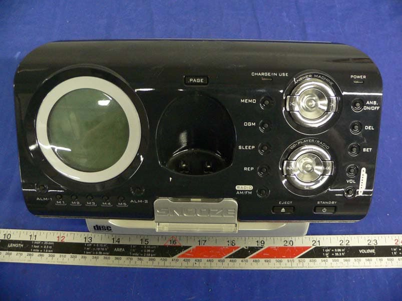
QFENTP3422
Jul 06, 20052.4GHz Digital Cordless Telephone
Equipment Class
DSS - Part 15 Spread Spectrum Transmitter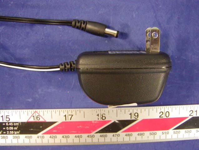
QFE35135
Sep 22, 2003900MHz Cordless Telephone
Equipment Class
DXX - Part 15 Low Power Communication Device Transmitter
QFENTP-6309
Jan 14, 20032.4 GHz Cordless Phone
Equipment Class
DXX - Part 15 Low Power Communication Device Transmitter
QFEPMP-3850
Aug 27, 20022.4GHz Cordless Phone
Equipment Class
DXT - Part 15 Low Power Transceiver, Rx Verified