SW8WD2600Bluetooth Device
Good Way Technology Co., Ltd.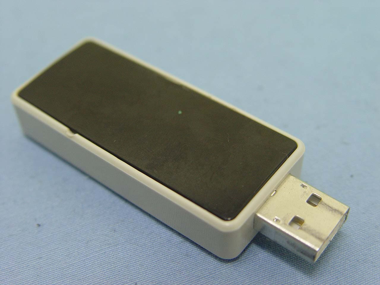
Click to zoom
Application Details
- Equipment Class
- DSS - Part 15 Spread Spectrum Transmitter
- Date of Grant
- Jul 12, 2006
- Application Purpose
- Original Equipment
- Date of Application
- Jul 12, 2006
- Equipment Note
- Bluetooth Device
- Frequency Range
- 2402.00000000 - 2480.00000000
- Country
- Taiwan
Documents & Files
Document Text
Text extracted from the exhibit documents filed with the FCC. Open a document above to read the original.
Users Manual
Wireless Solution for Skype LCD Wireless Skype phone SOLUTION: l 2.4GHz RF technology that allows you move freely while Skyping l distance : indoor > 15 M, outdoor > 30 M l Voice spec. Full duplex Toll quality (8KHz, 16bit voice) CVSD encode/decode for voice bits stream passing through host l Control functions Volume up-down/ mute Ringer Control interaction with Skype AP Numerical keys Telephone control-like keys l LCD display caller ID contact list and calling list l Compatible with VOIP solutions. ( Including Skype,MSN Messenger and Yahoo Messenger ) l Built in speaker and microphone l Implement Echo-elimination technology for quality sound l Buzzer function for incoming call alerts l Li-Polymer Battery recharged via USB l 5-types of hold music and 10 types of ringers l Built- in API commands for SKYPE system development USB interface: USB 1.1 compliant USB PnP, Meet USB audio class driver and HID class driver of Microsoft OS CONNECTOR: USB B type female connector RF SPEC: Compliant with BT 1.1 CLASS 1 RF out power : 36.64 mW Supports frequency hopping on 79 channels Up to seven simultaneous connections within effective range Transmitter power : +15.64 dBm for Dongle/ +16.6 dBm for Phone RSSI : -35 to -80 dBm RF interface baud rate 1Mbps transmit & receive Profile Support : headset, handfree , serial port(SPP), Generic Access Profile(GAP), and Service Discovery Profile(SDP) Adaptive Frequency Hopping (AFH), support for Bluetooth + Wi-Fi co-existence Speaker: Size: 13 mm Response Frequency: 300 ~ 3.4K Hz Output Impedance: 150 ohm Microphone: Sensitivity: - 40 +/- 2 dB Directivity: Onmidirectional Response Frequency: 20 ~ 20K Hz Operating Voltage: 5V (Bus-Powered) LCD DISPLAY: Resolution: 128 x32 pixels Display Mode : FSTN,POSITIVE,TRANSFULECTIVE Size: 31.0 X 19 mm Backlight: BLUE Multiple Languages: COMMAND-ENGLISH Traditional Chinese or Simplified Chinese Japanese Temperature: Operating: 0~40 °C Storage: -20~60 °C Humidity (Non-Condensing): Operating: < 90 % Storage: < 95 % Standby/talk time: 60 hours / 6 hours Battery capacity: 850 mAh Li-Polymer battery This device complies with Part 15 of the FCC Rules. Operation is subject to the following two conditions: (1) This device may not cause harmful interference. (2) This device must accept any interference received, including interference that maycause undesired operation. Any changes or modifications (including the antennas) made to this device that are not expressly approved by the manufacturer may void the users authority to operate the equipment. FCC RF Radiation Exposure Statement: This equipment complies with FCC RF radiation exposure limits set forth for an uncontrolled environment. This device and its antenna must not be co-located or operating in conjunction with any other antenna or transmitter.
Attestation Statements
Bluetooth Declaration Per FCC 15.247 Requirements 1 Output power and channel separation of a Bluetooth device in the different operating modes: The different operating modes (data-mode, acquisition-mode) of a Bluetooth device don’t influence the output power and the channel spacing. There is only one transmitter which is driven by identical input parameters concerning these two parameters. Only a different hopping sequence will be used. For this reason the check of these RF parameters in one op-mode is sufficient. 2 Frequency range of a Bluetooth device: Hereby we declare that the maximum frequency of this device is: 2402 – 2480 MHz. This is according the Bluetooth Core Specification V 1.0B (+ critical errata) for devices which will be operated in the USA. This was checked during the Bluetooth Qualification tests (Test Case: TRM/CA/04-E). Other frequency ranges ( e.g. for Spain, France, Japan) which are allowed according the Core Specification are not supported by this device. 3 Co-ordination of the hopping sequence in data mode to avoid simultaneous occupancy by multiple transmitters: Bluetooth units which want to communicate with other units must be organized in a structure called piconet. This piconet consist of max. 8 Bluetooth units. One unit is the master the other seven are the slaves. The master co-ordinates frequency occupation in this piconet for all units. As the master hop sequence is derived from it’s BD address which is unique for every Bluetooth device, additional masters intending to establish new piconets will always use different hop sequences. 4 Example of a hopping sequence in data mode: Example of a 79 hopping sequence in data mode: 40, 21, 44, 23, 42, 53, 46, 55, 48, 33, 52, 35, 50, 65, 54, 67, 56, 37, 60, 39, 58, 69, 62, 71, 64, 25, 68, 27, 66, 57, 70, 59, 72, 29, 76, 31, 74, 61, 78, 63, 01, 41, 05, 43, 03, 73, 07, 75, 09, 45, 13, 47, 11, 77, 15, 00, 64, 49, 66, 53, 68, 02, 70, 06, 01, 51, 03, 55, 05, 04 5 Equally average use of frequencies in data mode and behaviour for short transmissions: The generation of the hopping sequence in connection mode depends essentially on two input values: 1. LAP/UAP of the master of the connection 2. Internal master clock The LAP (lower address part) are the 24 LSB’s of the 48 BD_ADDRESS. The BD_ADDRESS is an unambiguous number of every Bluetooth unit. The UAP (upper address part) are the 24 MSB’s of the 48 BD_ADDRESS. The internal clock of a Bluetooth unit is derived from a free running clock which is never adjusted and is never turned off. For synchronisation with other units only offset are used. It has no relation to the time of the day. Its resolution is at least half the RX/TX slot length of 312.5 μs. The clock has a cycle of about one day (23h30). In most case it is implemented as 28 bit counter. For the deriving of the hopping sequence the entire LAP (24 bits), 4 LSB’s (4 bits) (Input 1) and the 27 MSB’s of the clock (Input 2) are used. With this input values different mathematical procedures (permutations, additions, XOR-operations) are performed to generate the sequence. This will be done at the beginning of every new transmission. Regarding short transmissions the Bluetooth system has the following behaviors: The first connection between the two devices is established, a hopping sequence was generated. For transmitting the wanted data the complete hopping sequence was not used. The connection ended. The second connection will be established. A new hopping sequence is generated. Due to the fact that the Bluetooth clock has a different value, because the period between the two transmission is longer (and it cannot be shorter) than the minimum resolution of the clock (312.5 μs). The hopping sequence will always differ from the first one. 6 Receiver input bandwidth and behaviors for repeated single or multiple packets: The input bandwidth of the receiver is 1 MHz. In every connection one Bluetooth device is the master and the other one is the slave. The master determines the hopping sequence (see chapter 5). The slave follows this sequence. Both devices shift between RX and TX time slot according to the clock of the master. Additionally the type of connection (e.g. single or multislot packet) is set up at the beginning of the connection. The master adapts its hopping frequency and its TX/RX timing according to the packet type of the connection. Also the slave of the connection will use these settings. Repeating of a packet has no influence on the hopping sequence. The hopping sequence generated by the master of the connection will be followed in any case. That means, a repeated packet will not be send on the same frequency, it is send on the next frequency of the hopping sequence. 7 Dwell time in data mode The dwell time of 0.3797s within a 30 second period in data mode is independent from the packet type (packet length). The calculation for a 30 second period is a follows: Dwell time = time slot length * hop rate / number of hopping channels *30s Example for a DH1 packet (with a maximum length of one time slot) Dwell time = 625 μs * 1600 1/s / 79 * 30s = 0.3797s (in a 30s period) For multislot packet the hopping is reduced according to the length of the packet. Example for a DH5 packet (with a maximum length of five time slots) Dwell time = 5 * 625 μs * 1600 * 1/5 *1/s / 79 * 30s = 0.3797s (in a 30s period) This is according the Bluetooth Core Specification V 1.0B (+ critical errata) for all Bluetooth devices. There for all Bluetooth devices comply with the FCC dwell time requirement in data mode. This was checked during the Bluetooth Qualification tests. The Dwell time in hybrid mode is measured and stated in the test report. 8 Channel Separation in hybrid mode The nominal channel spacing of the Bluetooth system is 1Mhz independent of the operating mode. The maximum “initial carrier frequency tolerance” which is allowed for Bluetooth is fcenter = 75 kHz. This was checked during the Bluetooth Qualification tests (Test Case:…
Text truncated - open the document above for the full version.
Cover Letter(s)
Date: 2006/3/7 Compliance Certification Services Certification Division 561F Monterey Road Morgan Hill, CA 95037 To whom it may concern: We, the undersigned, hereby authorize the Taiwan office of Compliance Engineering Services, Inc., d.b.a. Compliance Certification Services and hereafter referred to as CCS TW, to act on our behalf in all manners relating to application for equipment authorization, including signing of all documents relating to these matters. Any and all acts carried out by CCS TW on our behalf shall have the same effect as acts of our own. We, the undersigned, hereby certify that we are not subject to a denial of federal benefits, that includes FCC benefits, pursuant to Section 5301 of the Anti-Drug Abuse Act of 1988, 21 U.S.C. 853(a). In authorizing CCS TW as our agent, we still recognize that we are responsible to: a) Comply with the relevant provisions of the certification program; b) Make all necessary arrangements for the conduct of the evaluation, including provision for examining documentation and access to all areas, records (including internal audit reports) and personnel for the purposes of evaluation (e.g. testing, inspection, assessment, surveillance, reassessment) and resolution of complaints; c) Make claims regarding certification only in respect of the scope for which certification has been granted; d) Do not use our product certification in such a manner as to bring the Certification Division into disrepute and not make any statement regarding our product certification which the Certification Division may consider misleading or unauthorized; e) Upon suspension or cancellation of certification, discontinue use of all advertising matter that contains any reference thereto and return any certification documents as required by the Certification Division; f) Use certification only to indicate the products are certified as being in conformity with specified standards; g) Endeavor to ensure that no certificate or report nor any part thereof is used in a misleading manner; h) Ensure that any reference to our product certification in communication media such as documents, brochures or advertising, complies with the requirements of the Certification Division; i) Keep a record of all complaints made known to the us relating to the product compliance with requirements of the relevant standard and to make these records available to the Certification Division when requested; j) Take appropriate action with respect to such complaints and any deficiencies found in products or services that affect compliance with the requirements for certification; k) Document the actions taken. This authorization is valid until further written notice from the applicant. Sincerely Yours, ------------------------------- REMARK: 1. This authorization letter will be sent along with your application when filing with the Certification Division. 2. Please follow the format and type it on company letterhead and send original to us.
Cover Letter(s)
June 14, 2006 Federal Communications Commission Authorization and Evaluation Division FCC ID:SW8WD2600 Confidentiality Request Pursuant to Sections 0.457 and 0.459 of the Commission’s Rules, the Applicant hereby requests confidential treatment of information accompanying this Application as outlined below: 1. Schematics 2. Operational Description 3. Block Diagram The above materials contain trade secrets and proprietary information not customarily released to the public. The public disclosure of these matters might be harmful to the Applicant and provide unjustified benefits to its competitors. The Applicant understands that pursuant to Rule 0.457, disclosure of this Application and all accompanying documentation will not be made before the date of the Grant for this application. Sincerely, -------------------------------------------------
Cover Letter(s)
Helen Zhao Subject: FW: FW: GOOD WAY TECHNOLOGY CO., LTD., FCC ID: SW8WD2600, Assessment NO.: AN06T5874, Notice#1 7/13/2006 From: amanda.wu [mailto:[email protected]]On Behalf Of application Sent: Monday, June 26, 2006 10:14 PM To: Helen Zhao Subject: Re:FW: GOOD WAY TECHNOLOGY CO., LTD., FCC ID: SW8WD2600, Assessment NO.: AN06T5874, Notice#1 Dear Helen: Please see my reply, thank you. Best Regards Amanda -----Original Message----- Sent: Wednesday, June 21, 2006 6:35 PM Subject: GOOD WAY TECHNOLOGY CO., LTD., FCC ID: SW8WD2600, Assessment NO.: AN06T5874, Notice#1 Question #1: This is for your information: the SAR test was done at low channel, which yield the highest power, you might follow the (draft) test procedure, this is being reviewed now, still not finalized. The current valid procedure documented in Supplement C of OET Bulletin 65 specifies the test should be done at middle channel first. Before any new procedure is released, please still follow Supplement C of OET Bulletin 65. Ans: Thank you for your suggestion, I'll forward to engineer. Question #2: This device is not a bluetooth device, based upon Theory of Operation, it is "Similar to Bluetooth", in that case, please address the following four requirements as specified in FCC15.247(a)(1): a) Pseudorandom Frequency Hopping Sequence Describe how the hopping sequence is generated. Provide an example of the hopping sequence channels, in order to demonstrate that the sequence meets the requirement specified in the definition of a frequency hopping spread spectrum system, found in Section 2.1. b) Equal Hopping Frequency Use Describe how each individual EUT meets the requirement that each of its hopping channels is used equally on average (e.g., that each new transmission event begins on the next channel in the hopping sequence after the final channel used in the previous transmission event). c) System Receiver Input Bandwidth Describe how the associated receiver(s) complies with the requirement that its input bandwidth (either RF or IF) matches the bandwidth of the transmitted signal. d) System Receiver Hopping Capability Describe how the associated receiver(s) has the ability to shift frequencies in synchronization with the transmitted signals. Ans: Please see the revised OpDes. Best Regards, Helen Zhao The items indicated above must be submitted before processing can continue on the above referenced application. Failure to provide the requested information within 30 days of the original e-mail date may result in application dismissal and forfeiture of the filing fee. Also, please note that partial responses increase processing time and should not be submitted. Any questions about the content of this correspondence should be directed to the e-mail address listed below the name of the sender. 7/13/2006
External Photos
Compliance Certification Services Inc. Report No: 60522001 Date of Issue: June 6, 2006 Page 1 Total Page: 3 Rev. 00 EXTERNAL PHOTOGRAPHS OF EUT
Internal Photos
Compliance Certification Services Inc. Report No: 60522001 Date of Issue: June 6, 2006 Page 2 Rev.00 INTERNAL PHOTOGRAPHS OF EUT Compliance Certification Services Inc. Report No: 60522001 Date of Issue: June 6, 2006 Page 3 Rev.00
Parts List/Tune Up Info
G G a a i i n n F F o o r r c c e e T T e e c c h h n n o o l l o o g g y y C C o o . . , , L L t t d d A A P P P P R R O O V V A A L L S S H H E E E E T T Antenna MODEL NAME AT7020-E3R0HBAT PART NUMBER CUSTOMER GainForce VENDOR MODEL 028221-6858 ACCESSORIES SPECIFICATION SAMPLE DRAWING TEST REPORT APPROVED STATUS ACX Advanced Ceramic X Features v Monolithic SMD with small, low-profile and light-weight type. v Wide bandwidth Applications v2.4GHz WLAN, Home RF, Bluetooth Modules, etc. Specifications Part Number Frequency Range (MHz) Peak Gain (dBi typ.) Average Gain (dBi typ.) VSWR Impedance AT7020 -E3R0HBA_ 2400~2500 0dBi (XZ-V) -2dBi (XZ-V) 2 max. 50 Ω Q’ty/Reel (pcs) : 1,000 pcs Operating Temperature Range : -40 ~ +85 o C Storage Temperature Range : -40 ~ +85 o C Power Capacity : 3W max. Part Number Å Type AT : Antenna Ç Dimensions ( L × W ) 7.0× 2.0 mm É Material Code E Ñ Frequency Range 3R0=3000MHz Ö Specification Code HBA Ü Packaging T: Tape & Reel B: Bulk Terminal Configuration No. Terminal Name No. Terminal Name Å Feeding Point É NC Ç NC Ñ NC AT7020 Series Multilayer Chip Antenna AT 7020 - E 3R0 HBA p ÅÇ ÉÑÜÖ Å Ç É Ñ ACX Advanced Ceramic X Dimensions and Recommended PC Board Pattern Mark L W L1 W1 T a Dimensions 7.00.2 2.00.2 2.60.2 0.50.2 2.0+ 0.1/-0.2 0.50.3 (a) Without Matching Circuits (Unit in mm) (b) With Matching Circuits *Line width should be designed to match 50Ω characteristic impedance, depending on PCB material and thickness. Unit : mm a T (Matching circuit and component values will be different, depending on PCB layout) L W L1 W1 0.83 2.8 1 1.6 1.6 1 0.8 0.82 0.8 1 1 2 2 10 3.86 0 Ohm 0.83 2.8 1 1.6 1.6 1 0.8 0.82 0.8 1 1 2 2 10 3.86 2.2 nH 1.5 nH ACX Advanced Ceramic X Typical Electrical Characteristics (T=25 o C) vTest Board (Unit in mm) vReturn Loss(With Matching Circuits) 3.86 40 20 Ground No Ground 10 Antenna ACX Advanced Ceramic X vRadiation Patterns XZ cut @2.45GHz Vertical Horizontal YZ cut @2.45GHz Vertical Horizontal XZ-V/XZ-H YZ-V/YZ-H XY cut @2.45GHz Vertical Horizontal XY-V/XY-H 180 o 270 o 0 o 90 o X Z Y XY-cut scanning direction 180 270 o 0 o 90 o X Z Y XZ-cut scanning direction 180 270 0 o 90 o X Z Y YZ-cut scanning direction Advanced Ceramic X Corp. 16 Tzu Chiang Road, Hsinchu Industrial District Hsinchu Hsien 303, Taiwan TEL:886-3-5987008 FAX:886-3-5987001 E-mail: [email protected] http://www.acxc.com.tw ACX Adv anced Ceram ic X Item Requirements Procedure Solderability 1. No apparent damage 2. More than 75% of the terminal electrode shall be covered with new solder 1. Preheat: 120± 5 o C 2. Solder: 230± 5 o C for 5± 1 sec Thermal shock (Temperature Cycle) 1. No apparent damage 2. Fulfill the electrical specification after test 1. One cycle/ step 1: 85 ± 5 o C for 20sec step 2: -40 ± 3 o C for 20sec 2. Cycle time: 30min 3. No. of cycles: 100 4. Recovery: 1-2hrs Heat Resistance 1. No apparent damage 2. Fulfill the electrical specification after test 1. Temperature: 85± 2 o C 2. Duration: 24±2hrs 3. Recovery: 1-2hrs Low Temperature Resistance 1. No apparent damage 2. Fulfill the electrical specification after test 1. Temperature: -40 o ± 5 o C 2. Duration: 24 ±2hrs 3. Recovery: 1-2hrs Humidity Resistance 1. No apparent damage 2. Fulfill the electrical specification after test 1. Temperature: 85± 2 o C 2. Humidity: 80% ~ 85% RH 3. Duration: 1000±48hrs 4. Recovery: 1-2hrs Soldering strength (Push strength) 1. 9.8N minimum 1. Solder specimen onto test jig. 2. Apply push force at 0.5mm/s until electrode pads are peeled off or ceramic are broken. Pushing force is applied to longitude direction Deflection (Bending) 1. No apparent damage 2. Fulfill the electrical specification 1. Solder specimen onto test jig (FR4, 0.8mm) using the recommend soldering profile. 2. Apply a bending force of 2mm deflection ` Drop Shock 1. No apparent damage 1. Dropped onto hard wood from height of 50 cm for 3 times ; each x,y and z direction except terminal direction Mechanical & Environmental Characteristics R230 Pressure Rod 90mm ACX Adv anced Ceram ic X Typical Soldering Profile Typical Soldering Profile for Lead-free Process Flow Soldering : Reflow Soldering : T e m p erature ( o C) 20s. 230 o C 180 o C 260C 5s, max. Time (s.) 60s, min. Pre-heating 30s. 230 o C 180 o C 250 o C 10s, max. Time (s.) 60s, min. Pre-heating T e m p erature ( o C) The sample must be pre-heated before soldering .The temperature difference between preheating and soldering must be within 150 . Notes The contents of this data sheet are subject to change without notice. Please confirm the specifications and delivery conditions when placing your order. ACX Advanced Ceramic X Taping Specifications Tape Dimensions (Unit: mm) φ1.55 +0.05 A’ t D 7.5 ± 0.1 1.75 ± 0.1 C T A B 16± 0.2 A A’ B C D t T 4.0 0.1 4.0 0.1 1.9 0.1 3.5 0.1 2.0 0.1 0.20 0.05 Max. 1.4 4.0 0.1 4.0 0.1 2.4 0.1 5.5 0.1 2.0 0.1 0.20 0.05 Max. 1.4 7020 4.0 0.1 4.0 0.1 2.4 0.1 7.3 0.1 2.0 0.1 0.22 0.05 Max. 1.55 7635 8.0 0.1 4.0 0.1 3.75 0.1 7.85 0.1 2.0 0.1 0.30 0.05 Max. 1.40 8516 4.0 0.1 4.0 0.1 1.85 0.1 8.70 0.1 2.0 0.1 0.25 0.05 Max. 1.40 9520 4.0 0.1 4.0 0.1 2.3 0.1 9.7 0.1 2.0 0.1 0.22 0.05 Max. 1.45 R130 8.0 0.1 4.0 0.1 3.35 0.1 10.35 0.1 2.0 0.1 0.25 0.05 Max. 1.40 Typ e 3216 5020 Quantity Type 3216 5020 7020 7635 8516 9520 R130 Quantity /per reel 3,000pcs 2,000 1,000 pcs 1,000 pcs 1000pcs 1,000 pcs 1,000 pcs Reel Dimensions (Unit: mm) 178 ± 2.0 60 ± 0.5 1.4 Label: Customer’s Name, ACX P/N, Q’ty, Date, ACX Corp. D:13.0 ± 0.3 2.0 ± 0.5 D:21.8 ± 0.8 Label 19.5 16.7 ± 0.3 Leader and Trailer Tape (Plastic material) Trailer End Trailer (80mm min.) Cover Tape Only 60mm min. Leader End Empty Compartments with Cover Tape (80mm min.) Peel-off Force Peelin g Direction Top Cover Tape Carrier Ta pe <10 0 Peel-off force should be in the range of 0.1 – 0.6 N at a peel-off speed of 30010 mm/min . ACX Adv anced Ceramic X Storage Conditions (1) Temperature: 15 ~35, relative humidity (RH): 45~75%. (2) Non-corrosive environment (3) Products should b…
Text truncated - open the document above for the full version.
RF Exposure Info
Compliance Certification Services Inc. Report No: 60522001-SF FCC ID: SW8WD2600 Date of Issue: May 12, 2006 Note: This report shall not be reproduced except in full, without the written approval of Compliance Certification Services Inc. This document may be altered or revised by Compliance Certification Services Inc. personnel only, and shall be noted in the revision section of the document. Page 1 Total Page: 24 Rev. 00 ANSI/IEEE Std. C95.1-1992 in accordance with the requirements of FCC Report and Order: ET Docket 93-62, and OET Bulletin 65 Supplement C FCC TEST REPORT For Bluetooth Device Trade Name: GOOD WAY Model: WD2600 Issued to GOOD WAY TECHNOLOGY CO., LTD. 3F, No. 135, Lane 235, Pau Chiao Rd., Hsin-Tien City, Taipei Hsien, Taiwan, R.O.C. Issued by Compliance Certification Services Inc. No. 11, Wu-Kung 6 Rd, Wu-Ku Hsiang, Wu-Ku Industrial District, Taipei Hsien, (248) Taiwan. http://www.ccsemc.com.tw [email protected] Compliance Certification Services Inc. Report No: 60522001-SF Date of Issue: May 12, 2006 Page 2 Rev. 00 TABLE OF CONTENTS 1. EUT DESCRIPTION ..................................................................................................................4 2. REQUIREMENTS FOR COMPLIANCE TESTING DEFINED BY THE FCC .................5 3. DOSIMETRIC ASSESSMENT SYSTEM ................................................................................5 3.1 MEASUREMENT SYSTEM DIAGRAM .........................................................................6 3.2 SYSTEM COMPONENTS.................................................................................................7 4. EVALUATION PROCEDURES ...............................................................................................9 5. MEASUREMENT UNCERTAINTY ......................................................................................13 6. EXPOSURE LIMIT ..................................................................................................................14 7. TYPICAL COMPOSITION OF INGREDIENTS FOR LIQUID TISSUE PHANTOMS .14 8. MEASUREMENT RESULTS..................................................................................................15 8.1 SYSTEM PERFORMANCE CHECK..............................................................................15 8.2 TEST LIQUID CONFIRMATION...................................................................................16 8.3 EUT TUNE-UP PROCEDURES AND TEST MODE.....................................................17 8.4 SAR MEASUREMENTS RESULTS...............................................................................18 9. EUT PHOTOS ...........................................................................................................................21 10. EQUIPMENT LIST & CALIBRATION STATUS................................................................22 11. FACILITIES..............................................................................................................................23 12. REFERENCES ..........................................................................................................................23 13. ATTACHMENTS......................................................................................................................24 Compliance Certification Services Inc. Report No: 60522001-SF Date of Issue: May 12, 2006 Page 4 Rev. 00 1. EUT DESCRIPTION Product Bluetooth Device Trade Name GOOD WAY Model Number WD2600 Model Discrepancy N/A Frequency Range 2400 ~ 2483.5 MHz Max. O/P Power: (Conducted/Average) 9.41dBm Max. SAR (1g): 0.133 W/kg Modulation Technique FHSS (GFSK) Antenna Specification Antenna type: Chip antenna Battery option: Only one type / model with EUT Host ASUS , Model: L3400Tp , SN:2ANP048609 Remark: The sample selected for test was prototype that approximated to production product and was provided by manufacturer. Compliance Certification Services Inc. Report No: 60522001-SF Date of Issue: May 12, 2006 Page 5 Rev. 00 2. REQUIREMENTS FOR COMPLIANCE TESTING DEFINED BY THE FCC The US Federal Communications Commission has released the report and order “Guidelines for Evaluating the Environmental Effects of RF Radiation", ET Docket No. 93-62 in August 1996 [1]. The order requires routine SAR evaluation prior to equipment authorization of portable transmitter devices, including portable telephones. For consumer products, the applicable limit is 1.6 mW/g for an uncontrolled environment and 8.0 mW/g for an occupational/controlled environment as recommended by the ANSI/IEEE standard C95.1-1992 [6]. According to the Supplement C of OET Bulletin 65 “Evaluating Compliance with FCC Guide-lines for Human Exposure to Radio frequency Electromagnetic Fields", released on Jun 29, 2001 by the FCC, the device should be evaluated at maximum output power (radiated from the antenna) under “worst-case” conditions for normal or intended use, incorporating normal antenna operating positions, device peak performance frequencies and positions for maximum RF energy coupling. 3. DOSIMETRIC ASSESSMENT SYSTEM These measurements were performed with the automated near-field scanning system DASY4 from Schmid & Partner Engineering AG (SPEAG). The system is based on a high precision robot (working range greater than 0.9 m) which positions the probes with a positional repeatability of better than ± 0.02 mm. Special E- and H-field probes have been developed for measurements close to material discontinuity, the sensors of which are directly loaded with a Schottky diode and connected via highly resistive lines to the data acquisition unit. The SAR measurements were conducted with the dosimetric probe EX3DV4-SN: 3554 (manufactured by SPEAG), designed in the classical triangular configuration and optimized for dosimetric evaluation. The probe has been calibrated according to the procedure with accuracy of better than ±10%. The spherical isotropy was evaluated with the procedure and found to be better than ±0.25 dB. The phanto…
Text truncated - open the document above for the full version.
RF Exposure Info
Date/Time: 5/12/2006 8:48:31 AM Test Laboratory: Compliance Certification Services Inc. D2450V2 SN-784 Body DUT: Dipole 2450 MHz; Type: D2450V2; Serial: D2450V2 - SN:784 Communication System: CW2450; Frequency: 2450 MHz;Duty Cycle: 1:1 Medium parameters used: f = 2450 MHz; σ = 1.94 mho/m; ε r = 51.6; ρ = 1000 kg/m 3 Phantom section: Flat Section Air Temperature:25.3 deg C;Liquid Temperature:24.2 deg C Area Scan Find Secondary Maximum Within 2dB and with a peak SAR value greater than 0.0012W/kg DASY4 Configuration: z Probe: EX3DV4 - SN3554; ConvF(6.12, 6.12, 6.12); z Sensor-Surface: 2.5mm (Mechanical Surface Detection)Sensor-Surface: 0mm (Fix Surface) z Electronics: DAE3 Sn427; Calibrated: 9/22/2005 z Phantom: SAM 34; Type: SAM V4.0; Serial: TP-1150 z Measurement SW: DASY4, V4.6 Build 23; Postprocessing SW: SEMCAD, V1.8 Build 161 Pin=250mW,d=10mm/Area Scan (6x6x1): Measurement grid: dx=15mm, dy=15mm Maximum value of SAR (measured) = 13.9 mW/g Pin=250mW,d=10mm/Zoom Scan (5x5x7)/Cube 0: Measurement grid: dx=7.5mm, dy=7.5mm, dz=5mm Reference Value = 96.9 V/m; Power Drift = -0.001 dB Peak SAR (extrapolated) = 27.1 W/kg SAR(1 g) = 13.2 mW/g; SAR(10 g) = 6.03 mW/g Maximum value of SAR (measured) = 18.5 mW/g Pin=250mW,d=10mm/Z Scan (1x1x21): Measurement grid: dx=20mm, dy=20mm, dz=5mm Maximum value of SAR (measured) = 18.9 mW/g Page1 Page2 Date/Time: 5/12/2006 7:28:01 PM Test Laboratory: Compliance Certification Services Inc. Bluetooth WD2600 Bottom Touch mode DUT: WD2600; Type: WD2600; Serial: N/A Communication System: Bluetooth; Frequency: 2402 MHz;Duty Cycle: 1:1 Medium parameters used: f = 2402 MHz; σ = 1.88 mho/m; ε r = 51.8; ρ = 1000 kg/m 3 Phantom section: Flat Section Air Temperature:25.3 deg C;Liquid Temperature:24.2 deg C Area Scan Find Secondary Maximum Within 2dB and with a peak SAR value greater than 0.0012W/kg DASY4 Configuration: z Probe: EX3DV4 - SN3554; ConvF(6.12, 6.12, 6.12); z Sensor-Surface: 2.5mm (Mechanical Surface Detection) z Electronics: DAE3 Sn427; Calibrated: 9/22/2005 z Phantom: SAM 12; Type: SAM V4.0; Serial: TP-1150 z Measurement SW: DASY4, V4.6 Build 23; Postprocessing SW: SEMCAD, V1.8 Build 161 Low CH00/Area Scan (5x9x1…
Text truncated - open the document above for the full version.
Contact Information
Applicant
Alex Lee(Manager)
Test Firm
Compliance Certification Services Inc.Harris Lai
Technical Specifications
| # | Rule Parts | Frequency Range | Power Output |
|---|---|---|---|
| 1 | 15C | 2.40 GHz - 2.48 GHz | 36.60 mW |
Other Applications from Good Way Technology Co., Ltd.
SW8SD42000N1
Mar 17, 2024Human Presence Sensor
Equipment Class
DTS - Digital Transmission System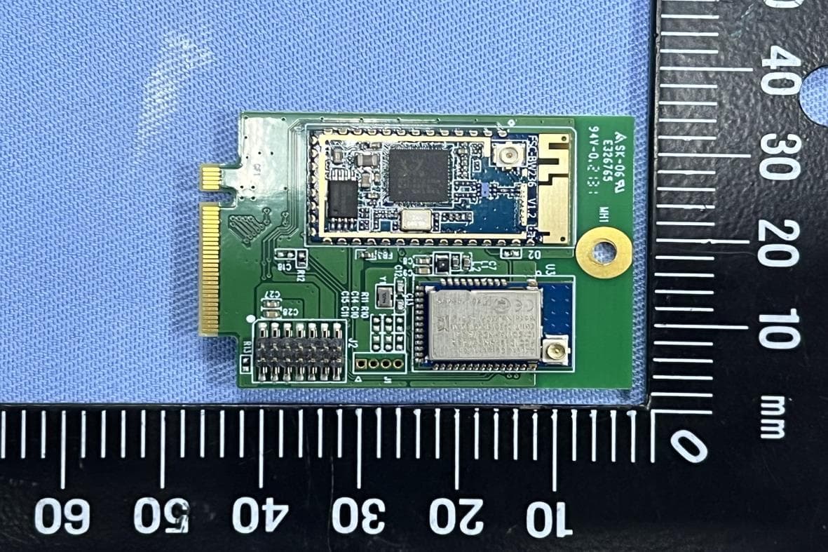
SW8TM51010
Jun 05, 2022Wi-Fi & BLE M.2 Wireless Module
Equipment Class
NII - Unlicensed National Information Infrastructure TX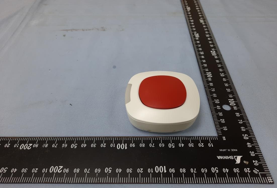
SW8TR1B100Z1S
Jul 12, 2020Scene Button
Equipment Class
DXX - Part 15 Low Power Communication Device Transmitter
SW8ZGATE
Oct 08, 2014802.11b/g/n and Z-WAVE
Equipment Class
DXX - Part 15 Low Power Communication Device Transmitter
SW8-WD9012R1
Sep 18, 2014HP Wireless Streaming Connector
Equipment Class
DTS - Digital Transmission System