V7TW900UWireless 11ac Dual-band USB Adapter
SHENZHEN TENDA TECHNOLOGY CO., LTD.
Click to zoom
Application Details
- Equipment Class
- NII - Unlicensed National Information Infrastructure TX
- Date of Grant
- Mar 22, 2013
- Application Purpose
- Original Equipment
- Date of Application
- Mar 22, 2013
- Equipment Note
- Wireless 11ac Dual-band USB Adapter
- Frequency Range
- 5210.00000000 - 5210.00000000
- Country
- China
Documents & Files
Document Text
Text extracted from the exhibit documents filed with the FCC. Open a document above to read the original.
Users Manual
Tenda Wireless Network Adapter User Guide Tenda Wireless Network Adapter User Guide Copyright Statement is the registered trademark of Shenzhen Tenda Technology Co., Ltd. All the products and product names mentioned herein are the trademarks or registered trademarks of their respective holders. Copyright of the whole product as integration, including its accessories and software, belongs to Shenzhen Tenda Technology Co., Ltd. Without the permission of Shenzhen Tenda Technology Co., Ltd, any individual or party is not allowed to copy, plagiarize, reproduce, or translate it into other languages. All the photos and product specifications mentioned in this guide are for references only. Upgrades of software and hardware may occur, and if there are changes, Tenda is not responsible for notifying in advance. If you would like to know more about our product information, please visit our website at www.tenda.cn . Tenda Wireless Network Adapter User Guide - 1 - Contents Chapter 1 Product Introduction......................................................... 2 1.1 Package Contents ............................................................................ 2 1.2 LED Indicator Description ................................................................. 2 1.3 Product Features..............................................................................3 1.4 Product Usage .................................................................................. 3 1.5 Before Installation ............................................................................. 4 1.6 Disable other manufacturers’ wireless network adapters .................. 4 1.7 Product Maintenance ........................................................................ 6 Chapter 2 Installation Guide.............................................................. 7 2.1 Hardware Installation ........................................................................ 7 2.2 Software Installation ......................................................................... 7 Chapter 3 How to use the Windows Built-in Wireless Configuration...... 15 3.1 Wireless Network Connection under Windows XP ......................... 15 3.2 Wireless Network Connection under Windows 7 ............................ 19 3.3 Wireless Network Connection under Windows 8 ............................ 21 Appendix 1: Acronyms and Terms.................................................... 25 Tenda Wireless Network Adapter User Guide - 2 - Chapter 1 Product Introduction Thank you for choosing this Tenda wireless adapter! The Tenda wireless adapter supports IEEE wireless standards, and is able to quickly process file transfer, video, multi-media and other applications that require higher bandwidth. This Tenda wireless adapter also integrates wireless configuration program, which makes it easy and quick to set up the wireless client. Besides, Soft AP is supported for fast wireless network establishment, and WPS encryption supported for you to quickly encrypt and secure your wireless network. All in all, the Tenda wireless adapter is easy-to-use, and of robust signal, long transmitting distance. 1.1 Package Contents One Wireless network adapter OneSoftwareCD(includesuserguideanddriver) The above list is for your reference only,the actual contents may differ according to the product you purchase. 1.2 LED Indicator Description There is one status LED indicator on the side of the wireless network adapter. It lights up and stays ON when working correctly, and flashes when transferring data. Tenda Wireless Network Adapter User Guide - 3 - 1.3 Product Features ¾Detects wireless network and adjusts transmitting rate automatically ¾Provides two working modes: Infrastructure and Ad-Hoc ¾Supports WEP data encryption and WPA-PSK/WPA2-PSK encryption methods ¾Supports WPS (Wi-Fi Protected Setup) encryption to secure your wireless network ¾Complies with Windows 7/XP/ 2000/Vista, Linux, MAC OS, etc. 1.4 Product Usage This Tenda Wireless Adapter offers a fast, reliable and extendable solution for wireless access. It is mostly used in the following circumstances: Enables staff members who require higher mobility, to have access to the wireless network anywhere inside their company. Enables wireless communication for companies or places which are not suitable for wired LAN installation because of budget or building environment restrictions, such as historical buildings, rentals, or places for short-term usage. Suitable for Enterprises or individuals requiring to regularly alter the networking topology Helps enterprises or individuals who would like to use wireless to establish wireless network quickly and frees them from the Tenda Wireless Network Adapter User Guide - 4 - trouble of cable distribution. 1.5 Before Installation 1.Please read through the whole user guide before you install and use this product. 2.Please close or uninstall the configuration programs of other manufacturers’ before you install the configuration programs of Tenda network adapters to avoid possible UI (user interface) conflict. 3.To avoid possible network conflicts between this Tenda network adapter and those of other manufactures’, we recommend that you first disable the network adapters of other manufacturers before installaing the driver. 1.6 Disable other manufacturers’ wireless network adapters 1. Right click “My Computer” and select“Manage” Tenda Wireless Network Adapter User Guide - 5 - 2. On the Computer Management screen ,select“Device Manager”-“Network adapters”, and right click the network adapter you want to disable and click “Disable” 3. Click the “Yes” button on the dialogue box to disable the Tenda Wireless Network Adapter User Guide - 6 - network adapter. 1.7 Product Maintenance Please keep the product away from water and humid environment to guarantee its normal performance Protect it against hazardous substances (such as acids, alkalis etc). Please don’t directly expose the adapter to the sunlight or excess…
Text truncated - open the document above for the full version.
External Photos
EXHIBIT B - EUT EXTERNAL PHOTOGRAPHS EUT –Top View EUT – Bottom View EUT – Uncover View EUT –Left View EUT – Right View
ID Label/Location Info
EXHIBIT A - FCC ID LABELING AND LOCATION FCC ID Label Proposed FCC ID Label Location The label shown shall be permanently affixed at a conspicuous location on the device and be readily visible to the user at the time purchase (Labeling requirements per 2.925) Label Here
Internal Photos
EXHIBIT B - EUT EXTERNAL PHOTOGRAPHS EUT –Cover Off View EUT –Main Board Top View EUT –Main Board Bottom View
Operational Description
SHENZHENTENDA TECHNOLOGYCO.LTD FCC ID:V7TW900U Operational Description This device is a Wireless 11AC Dual-band USB Adapter,Model:W900U, Which operates in 2.412-2462Ghz and5180-5240Mhz 5745-5825Mhz Band; The maximum data ratecouldbeupto 300Mbps which OFDM technique. If the signal to noise radio is too poor whichcould not support 300Mbps,the 11Mbps data rate with DSSS technique will be applied. The transmitter of the EUT is powered by (DC5V500maA) usb port, The device adapts DSSS and OFDM modulation.And the antenna was 3dbi PCB print antenna.And provided diversity function to improve the receiving functions.It allows your computerto connection to a wireless network and to share resources, SHENZHENTENDA TECHNOLOGYCO.LTD EUT General Description
RF Exposure Info
Bay Area Compliance Laboratories Corp. (Dongguan) Report No.: R2DG130130002-00C FCC Part 15.407 Page 8 of 139 FCC §15.407 (f) & §1.1307 (b) (1) & §2.1093- RF EXPOSURE Applicable Standard According to§15.407 (f) and §1.1307(b)(1), systems operating under the provisions of this section shall be operated in a manner that ensure that the public is not exposed to radio frequency energy level in excess of the Commission’s guideline. According to KDB 447498 D01 Mobile Portable RF Exposure V05 Appendix A, SAR can be exempted if the output power is less than the SAR exclusion threshold: For f=5200MHz, the output power is less 7mW at distance of 5mm. Measurement Result Peak conducted output power= 7.79 dBm Antenna gain = 3.0 dBi SAR exclusion threshold 7 mW (8.45 dBm) > 7.79 dBm So the SAR evaluation is not necessary.
Schematics
5 4 3 2 1 DCBA A TendaW900U Trade Name: Product Name: TENDA TitleSize Document Number Rev Date: Sheet of Cover Page V0.11 W900U A4 18 Monday, November 19, 2012 TitleSize Document Number Rev Date: Sheet of Cover Page V0.11 W900U A4 18 Monday, November 19, 2012 TitleSize Document Number Rev Date: Sheet of Cover Page V0.11 W900U A4 18 Monday, November 19, 2012 55 44 33 22 11 D D C C B B A A POPULATE FOR USB USB interface: DM, DP are USB signal. AVDD33 is pwr supply. MONCDR is a debug pin. RREF needs a ref. res. Pin chip default board default description C0_FEMCTRL_1 C1_FEMCTRL_0, C0_FEMCTRL_2 C1_FEMCTRL_1C2_FEMCTRL_0C2_FEMCTRL_2 BANDSEL gpio[7,6] gpio8 0,1110101,101 1,100110,11 1: 40MHz XTAL selected0: 20MHz XTAL selected0,1: 4k SROM size1,0: 16k SROM size0: Boot from SRAM1: Boot from ROM0: don't query OTP1: query OTP0: SROM not present (ATMEL if SFLASH is present)1: SROM present (ST if SFLASH is present)0: SFLASH not present1: SFLASH presentPCIe: see Twiki 1: USB 2.0 enable, PCIe disable (only in 12x12 package) 0: USB 2.0 disable, PCIe enable (only in 12x12 package) For B0, R8 need to depopulate for HT availabeR80 need to populate for sflash not present expose traces for cuttingTSSI0 --> I/Q test IPTSSI1 --> I/Q test INTSSI2 --> I/Q test QPRCAL_EXT_RES --> IQ test QN TENDA 定位孔 RF_DISABLE_L WPS SFLASH_CSSFLASH_CLKSFLASH_MISOSFLASH_MOSI WPS SFLASH_MOSISFLASH_CLKSFLASH_CS SFLASH_MISO GPIO_10GPIO_9 GPIO_10GPIO_9 VDD3_3 EXT_POR_L EXT_POR_L MONCDR X_IN X_OUT RXG_0RXG_1 RXA_0RXA_1 TXG_0TXG_1 TXA_0TXA_1 C0_FEM_CRXC2_FEM_CRXC2_PAENG_CC0_PAENG_CC1_PAENG_CC1_FEM_CRX TSSI_0TSSI_1 DP DN USB_DPUSB_DN USB_DPUSB_DNVDD5_USB C0_PAENA_CC1_PAENA_CFEM_BAND_SEL VDD3_3 VDD3_3 VDD3_3 VDD3_3 VDD3_3 VDD3_3 VDD3_3 VDD3_3 VDD3_3 VDD3_3 VDD3_3 VDD3_3 VDD5 RXG_0RXG_1RXA_0RXA_1TXG_0TXG_1TXA_0TXA_1 C0_PAENG_CC1_PAENG_CC1_FEM_CRXTSSI_0TSSI_1 C1_PAENA_C C0_PAENA_C C0_FEM_CRX FEM_BAND_SEL TitleSize Document Number Rev Date: Sheet of USB/Control Lines V0.11 W900U A2 58 Tuesday, February 19, 2013 TitleSize Document Number Rev Date: Sheet of USB/Control Lines V0.11 W900U A2 58 Tuesday, February 19, 2013 TitleSize Document Number Rev Date: Sheet of USB/Control Lines V0.11 W900U A2 58 Tuesday, February 19, 2013 R55 Res R55 Res R58 Res R58 Res C24CAPC24CAP R154 Res R154 Res HH1HH1 C70 CAP C70 CAP R52ResR52Res U1BU1B REFCLKP 98 REFCLKN 99 TDP0 104 TDN0 103 RDP0 106 RDN0 107 PERST_L 94 PCIE_CLKREQ_L 95 PCIE_PME_L 97 RF_DISABLE_L 92 SPROM_CS 91 SPROM_CLK/SECI_AUX 88 SPROM_DIN/SECI_IN 90 SPROM_DOUT/SECI_OUT 87 PTESTN 102 PTESTP 101 R45 Res R45 Res R51ResR51Res R59 Res R59 Res R57ResR57Res R12 Res R12 Res R54 Res R54 Res C64 CAP C64 CAP R56ResR56Res R157 Res R157 Res TP4TP4 R53 Res R53 Res D1 LED*1 D1 LED*1 1 2 R76ResR76Res C54 CAP C54 CAP TP5TP5 R11ResR11Res R42 Res R42 Res TP1TP1 C22CAPC22CAP C17CAPC17CAP R32 Res R32 Res C58CAPC58CAP R60 Res R60 Res R5 Res R5 Res SW1 sw_1 SW1 sw_1 2 1 3 4 D2 LED*1 D2 LED*1 1 2 R72 Res R72 Res C18CAPC18CAP R74ResR74Res RT9818C_0 U4 RT9818C_0 U4 VDD 3 GND 1 RST 2 MX25L32EZUI_0 U2 MX25L32EZUI_0 U2 SI/SIO0 5 SCLK 6 CS* 1 WP*/ACC 3 HOLD* 7 VCC 8 SO/SIO1 2 GND 4 HS 9 BCM43526KMLG U1A BCM43526KMLG U1A RF_2G_IN_CORE0 51 RF_2G_IN_CORE1 42 RF_2G_IN_CORE2 33 RF_2G_OUT_CORE0 54 RF_2G_OUT_CORE1 45 RF_2G_OUT_CORE2 36 RF_5G_OUT_CORE0 46 RF_5G_OUT_CORE1 37 RF_5G_OUT_CORE2 28 GPIO_0/TRST_L 69 GPIO_3/TDI 64 GPIO_2/TDO 65 GPIO_4/TMS 63 GPIO_1/TCK 67 GPIO_5/EXT_POR_L 85 GPIO_6/UART_RX 83 GPIO_7/UART_TX 82 GPIO_8 80 GPIO_9 79 GPIO_10 78 GPIO_11 77 JTAG_SEL 84 XTAL_IN 61 XTAL_OUT 60 XTAL_BUF_OUT 62 C0_FEMCTRL_0 8 C0_FEMCTRL_1 9 C0_FEMCTRL_2 11 C1_FEMCTRL_0 12 C1_FEMCTRL_1 13 C1_FEMCTRL_2 15 C2_FEMCTRL_0 16 C2_FEMCTRL_1 18 C2_FEMCTRL_2 19 FEM_BAND_SEL 20 O_PAVREF 73 O_PAVREF_CTL1 72 O_PAVREF_CTL2 71 O_PAVREF_CTL3 70 GPIO_0/TSSI_0 24 GPIO_1/TSSI_1 23 GPIO_2/TSSI_2 22 MONCDR 1 DP 2 DM 3 AVDD3P3 4 MONPLL 5 RREF 6 NC_26 26 NC_27 27 REF_5G_IN_CORE0 49 REF_5G_IN_CORE1 40 REF_5G_IN_CORE2 31 C23ResC23Res 2.5x3.2 Y1 XTAL_3.2x2.5 2.5x3.2 Y1 XTAL_3.2x2.5 12 43 R35 Res R35 Res R71 Res R71 Res R8 Res R8 Res TP3TP3 INDUCTOR_0 FB6 INDUCTOR_0 FB6 1 2 HH3HH3 J3USB_U5M_6PINJ3USB_U5M_6PIN VBUS 1 D- 2 D+ 3 ID 4 SHILD1 5 SHILD2 6 HH2HH2 R80 Res R80 Res C80 CAP C80 CAP TP2TP2 55 44 33 22 11 D D C C B B A A place near pin20 place near pin21 place near pin9 place near pin20 place near pin21 place near pin9 MUST BE SHORT MUST BE SHORT Switch Control Logic Table for FEMs Mode C0 C1 ENA ENGrxgtxg rxg bypass rxatxa rxa bypass 0000 000 00000 00000 1 1111 1 1 TENDA 50 OHMs 50 OHMs 50 OHMs 50 OHMs VDD_FEM RXG_0RXA_0 TSSI_0 WLAN0_RF VTXA0FVRXA0F C0_FEM_CRXFEM_BAND_SEL C0_PAENGC0_PAENA VDD_FEM RXG_1RXA_1 TSSI_1 WLAN1_RF VTXA1FVRXA1F C1_FEM_CRXFEM_BAND_SEL C1_PAENGC1_PAENA C0_PAENG C0_PAENG_C C0_PAENA C0_PAENA_C C1_PAENG C1_PAENG_C C1_PAENA C1_PAENA_C VDD_FEM VDD3_3 RXG_0RXA_0 TXG_0TXA_0 TSSI_0 C0_FEM_CRXFEM_BAND_SEL RXG_1RXA_1 TXG_1TXA_1 TSSI_1 C1_FEM_CRXFEM_BAND_SEL C0_PAENG_CC1_PAENG_C C0_PAENA_CC1_PAENA_C TitleSize Document Number Rev Date: Sheet of RF Front End V0.11 W900U A3 68 Tuesday, February 19, 2013 TitleSize Document Number Rev Date: Sheet of RF Front End V0.11 W900U A3 68 Tuesday, February 19, 2013 TitleSize Document Number Rev Date: Sheet of RF Front End V0.11 W900U A3 68 Tuesday, February 19, 2013 R18 Res R18 Res C321CAPC321CAP C7 CAP C7 CAP C8CAPC8CAP C322CAPC322CAP C104 CAP C104 CAP C28CAPC28CAP C218CAPC218CAP R4 Res R4 Res R19 Res R19 Res C13 CAP C13 CAP SKY85803_0 U11 SKY85803_0 U11 VCC1 9 VCC2 10 VCC3 20 VCC4 21 RG 15 RA 16 TG 13 DET 22 TA 18 GND7 14 GND8 17 GND9 23 GND10 24 HS-GND 25 ANT 4 C1 6 C0 7 ENG 1 ENA 19 GND1 2 GND2 3 GND3 5 GND4 8 GND5 11 GND6 12 L4INDUCTORL4INDUCTOR SKY85803_1 U10 SKY85803_1 U10 VCC1 9 VCC2 10 VCC3 20 VCC4 21 RG 15 RA 16 TG 13 DET 22 TA 18 GND7 14 GND8 17 GND9 23 GND10 24 HS-GND 25 ANT 4 C1 6 C0 7 ENG 1 ENA 19 GND1 2 GND2 3 GND3 5 GND4 8 GND5 11 GND6 12 C27CAPC27CAP C25 Res C25 Res R7 Res R7 Res C11CAPC11CAP C14CAPC14CAP C217CAPC217CAP C101CAPC101CAP L5INDUCTORL5INDUCTOR R24 Res R24 Res R6 Res R6 Res C10CAPC…
Text truncated - open the document above for the full version.
Test Report
Note: This test report is prepared for the customer shown above and for the device described herein. It may not be duplicated or used in part without prior written consent from Bay Area Compliance Laboratories Corp. (Dongguan). FCC PART 15.407 TEST REPORT For SHENZHEN TENDA TECHNOLOGY CO.,LTD. Tenda Industrial Park, No. 34-1, Shilong Rd., Shiyan Town, Bao'an District, Shenzhen, P.R.China Report Type: Original Report Product Type: Wireless 11ac Dual-band usb Adapter Test En gineer: Leon Chen Re port Number: R2DG130130002-00C Re port Date: 2013-03-14 Reviewed By: Ivan Cao RF Leader Test Laboratory: Bay Area Compliance Laboratories Corp. (Dongguan) No.69 Pulongcun, Puxinhu Industrial Zone, Tangxia, Dongguan, Guangdong, China Tel: +86-769-86858888 Fax: +86-769-86858891 www.baclcorp.com.cn FCC ID: V7TW900U Bay Area Compliance Laboratories Corp. (Dongguan) Report No.: R2DG130130002-00C FCC Part 15.407 Page 2 of 139 TABLE OF CONTENTS GENERAL INFORMATION ....................................................................................................................................... 4 PRODUCT DESCRIPTION FOR EQUIPMENT UNDER TEST (EUT) ..................................................................................... 4 OBJECTIVE ................................................................................................................................................................... 4 RELATED SUBMITTAL(S)/GRANT(S) ............................................................................................................................. 4 TEST METHODOLOGY .................................................................................................................................................. 4 TEST FACILITY ............................................................................................................................................................. 4 SYSTEM TEST CONFIGURATION .......................................................................................................................... 5 DESCRIPTION OF TEST CONFIGURATION ...................................................................................................................... 5 EUT EXERCISE SOFTWARE .......................................................................................................................................... 5 EQUIPMENT MODIFICATIONS ....................................................................................................................................... 5 SUPPORT EQUIPMENT LIST AND DETAILS .................................................................................................................... 5 EXTERNAL CABLE ........................................................................................................................................................ 6 PRINTER ....................................................................................................................................................................... 6 KEYBOARD .................................................................................................................................................................. 6 BLOCK DIAGRAM OF TEST SETUP ................................................................................................................................ 6 SUMMARY OF TEST RESULTS ............................................................................................................................... 7 FCC §15.407 (f) & §1.1307 (b) (1) & §2.1093- RF EXPOSURE .................................................................................... 8 APPLICABLE STANDARD .............................................................................................................................................. 8 FCC §15.203 – ANTENNA REQUIREMENT ............................................................................................................ 9 APPLICABLE STANDARD .............................................................................................................................................. 9 ANTENNA CONNECTOR CONSTRUCTION ...................................................................................................................... 9 FCC §15.407 (b) (6) §15.207 (a) – CONDUCTED EMISSIONS ............................................................................. 10 APPLICABLE STANDARD ............................................................................................................................................ 10 MEASUREMENT UNCERTAINTY .................................................................................................................................. 10 EUT SETUP ................................................................................................................................................................ 11 EMI TEST RECEIVER SETUP ....................................................................................................................................... 11 CORRECTED AMPLITUDE & MARGIN CALCULATION ................................................................................................. 11 TEST EQUIPMENT LIST AND DETAILS ......................................................................................................................... 12 TEST PROCEDURE ...................................................................................................................................................... 12 TEST RESULTS SUMMARY .......................................................................................................................................... 12 TEST DATA ................................................................................................................................................................ 12 FCC §15.209, §15.205 & §15.407(b) (1) (6) (7) – UNDESIRABLE EMISSION & RESTRICTED BANDS ....... 15…
Text truncated - open the document above for the full version.
Test Setup Photos
EXHIBIT D - TEST SETUP PHOTOGRAPHS Conducted Emissions - Front View Conducted Emissions – Rear View Radiated Emission -Front View Radiated Emission - Rear View Radiated Emission Above 1GHz-Front View Radiated Emission Above 1GHz-Rear View
Contact Information
Applicant
Shen Yue(Engineer)
Test Firm
Bay Area Compliance Laboratories Corp. (Dongguan)John Chan
[email protected]86-769-86858888
Technical Specifications
| # | Rule Parts | Frequency Range | Power Output |
|---|---|---|---|
| 3 | 15E | 5.21 GHz - 5.21 GHz | 6.00 mW |
Other Applications from SHENZHEN TENDA TECHNOLOGY CO., LTD.
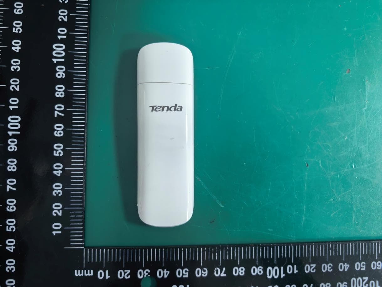
V7TU18V3
Aug 26, 2026AX1800 Wi-Fi 6 Dual-Band USB Adapter
Equipment Class
NII - Unlicensed National Information Infrastructure TX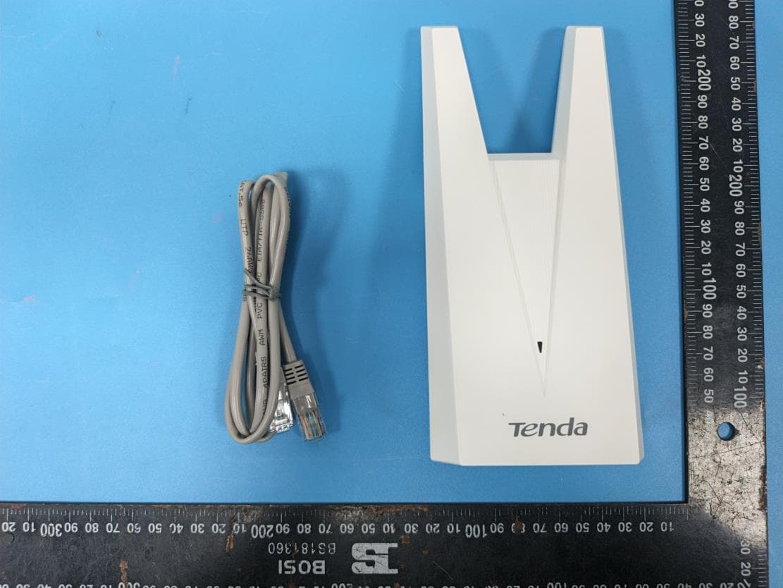
V7TA33V2
Aug 25, 2026AX3000 Dual-Band Gigabit Wi-Fi Range Extender, AX1800 Dual-Band Gigabit Wi-Fi Range Extender
Equipment Class
DTS - Digital Transmission System
V7TCH9V2
Jul 20, 20266MP Dual-lens Linkage Wi-Fi Pan/Tilt Camera
Equipment Class
DTS - Digital Transmission System
V7TCH3V21
Jul 14, 20263MP Wi-Fi Pan/Tilt Camera
Equipment Class
DTS - Digital Transmission System
V7TCP3P1
Jun 30, 20263MP Security Pan/Tilt Camera
Equipment Class
DTS - Digital Transmission System