VIYCFU0321802.15.4 ZigBee RF Module
Hosiden Corporation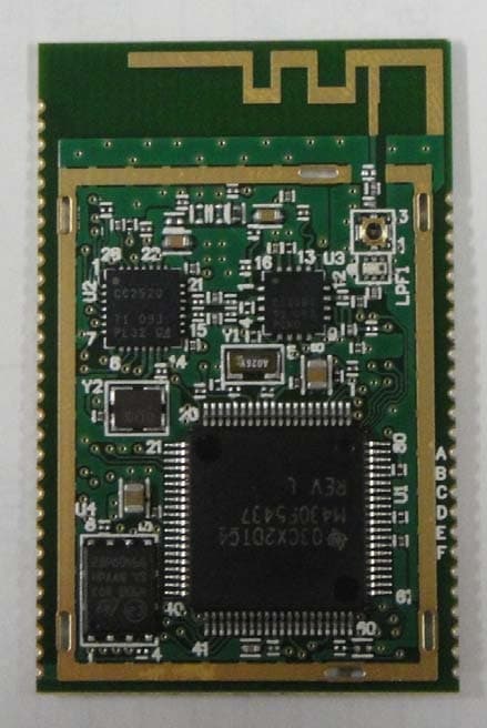
Click to zoom
Application Details
- Equipment Class
- DSS - Part 15 Spread Spectrum Transmitter
- Date of Grant
- May 17, 2012
- Application Purpose
- Original Equipment
- Date of Application
- May 17, 2012
- Equipment Note
- 802.15.4 ZigBee RF Module
- Frequency Range
- 2405.00000000 - 2480.00000000
- Company
- Hosiden Corporation
- Country
- Japan
Documents & Files
Document Text
Text extracted from the exhibit documents filed with the FCC. Open a document above to read the original.
Users Manual
4-33, Kitakyuhoji 1-chome, Yao-City, Osaka, 581-0071, Japan User Guide for CFU0321 RF Module Specification for the CFU0321 Smart Energy RF module based on the IEEE 802.15.4 and ZigBee specifications Draft v.0.1 2011-4-24 4-33, Kitakyuhoji 1-chome, Yao-City, Osaka, 581-0071, Japan Table of Contents CFU0321 RF Module Description The CFU0321 is a general purpose IEEE 802.15.4 RF module designed with Smart Energy applications in mind. It features the TI CC2520 RF transceiver, TI CC2591 2.4GHz Power Amplifier, I MSP 430F5437 microcontroller with 256K of flash RAM and 16K of RAM, 1MB external flash RAM, and pattern antenna. Depending on the SKU, the following options are available: • Board to Board connector • Side through hole for surface mounted The CFU0321 is designed to be surface mounted; however, board to board connector is standard feature and allows Board to Board connector to be attached for easy socketing. The unit requires 2.7V – 3.6V unregulated DC supply; internal voltage regulation supplies the radio. The nominal transmission and reception distance is 100 meters with the on-board pattern antenna. TI Z-Stack 2.4 port is available for the CFU0321, along with an implementation of the Smart Energy profile device(s). Also, the TIMAC only firmware is available. Standard development environment requires the MSP430 version of the IAR IDE toolset. Programming the CFU0321 requires the HVE0704, the development board specifically designed for the CFU0321. Additionally a JTAG programmer is required. Applications The CFU0321 allows devices to join the ZigBee SE 1.x network currently being deployed by the utility companies. The following 4-33, Kitakyuhoji 1-chome, Yao-City, Osaka, 581-0071, Japan are some applications of the CFU0321 RF module. Energy Service Portal Utility Meters Gateway Devices Home Automation Devices Load Control Devices Telecom Applications In-home Displays Health care products Reference firmware implementations are available for various devices. For details, please contact Wireless Glue Networks, Inc. CFU0321 Key Features The CFU0321 is a general purpose IEEE 802.15.4 RF module based on the TI CC2520, CC2591 and MSP430. The module also includes a serial 1MB Flash RAM as standard. Module Overview The CFU0321 is an IEEE 802.15.4 RF module optimized for the Smart Energy 1.x feature set requirements from the ZigBee Alliance. The module provides turnkey implementation of the ZigBee 2007 platform based on the Z-Stack 2.4x, and ZigBee MSP430F5437 Serial Flash RAM CC2520 RF CC2591 PA Pattern Antenna RF Connector With Switch 4-33, Kitakyuhoji 1-chome, Yao-City, Osaka, 581-0071, Japan Cluster Library, along with the required device firmware (e.g. In-home Display, etc.). The CFU0321 has been tested with the Smart Energy Device Simulator, the validated test harness solution for the ZigBee Alliance for Smart Energy 1.0 Application Profile, and therefore assured of interoperability with all major devices supporting Smart Energy application profiles. Specifications Development Board Schematic Layout Information The best way to incorporate CFU0321 into devices is to implement the electrical connections as described on the HVE0704 development board. The schematic for the development board is given below. Operating conditions 4-33, Kitakyuhoji 1-chome, Yao-City, Osaka, 581-0071, Japan Parameter Min Max Unit Operating Voltage 2.7 3.6 V Operating Temperature -20 60 °C Electrical Characteristics Parameter Condition Typ Unit Transmission Current TXPOWER = 0xF9 140 mA Receive Current HGM = 1 35 mA Transmit Power TXPOWER = 0xF9 17 dBm TXPOWER = 0x2C 10 dBm Receive Sensitivity HGM = 1 -96 dBm Mounting Information The following diagram serves as guidance in incorporating the CFU0321 module onto other circuit boards. The following is for Board-to-Board connector equipped version of the module. It is important to note that the ground plane should be absent directly beneath the pattern antenna. 4-33, Kitakyuhoji 1-chome, Yao-City, Osaka, 581-0071, Japan Pin Assignment and Layout CFU0321 Pin Assignments PIN ID Function I/ODescription 1 GND1 2 P2.0/TA1CLK/MCLK I/O General-purpose digital I/O with port interrupt TA1 clock signal TA1CLK input MCLK output 3 P2.1/TA1.0 I/O General-purpose digital I/O with port interrupt TA1 CCR0 capture: CCI0A input, compare: Out0 output 4 P2.3/TA1.2 I/O General-purpose digital I/O with port interrupt TA1 CCR1 capture: CCI1A input, compare: Out1 output 5 P2.4/RTCCLK I/O General-purpose digital I/O with port interrupt RTCCLK output 6 P2.5/ROSC I/OGeneral-purpose digital I/O with port interrupt 7 P2.6/ACLK I/O General-purpose digital I/O with port interrupt ACLK output (divided by 1, 2, 4, 8, 16, or 32) 8 P2.7/ADC12CLK/DMAE0 I/O General-purpose digital I/O with port interrupt Conversion clock input ADC DMA external trigger input 9 P3.0/UCB0STE/UCA0CLK I/O General-purpose digital I/O Slave transmit enable – USCI_B0 SPI mode P3.0/UCB0STE/UCA0CLK 33 35 L5 I/O Clock signal input – USCI_A0 SPI slave mode Clock signal output – USCI_A0 SPI master mode 10 P3.1/UCB0SIMO/ UCB0SDA/[FLASH_SIMO] I/O General-purpose digital I/O Slave in, master out – USCI_B0 SPI mode I2C data – USCI_B0 I2C mode 4-33, Kitakyuhoji 1-chome, Yao-City, Osaka, 581-0071, Japan PIN ID Function I/ODescription 11 P3.2/UCB0SOMI/ UCB0SCL/[FLASH_SOMI] I/O General-purpose digital I/O P3.2/UCB0SOMI/UCB0SCL 35 37 J6 I/O Slave out, master in – USCI_B0 SPI mode I2C clock – USCI_B0 I2C mode 12 P3.3/UCB0CLK/UCA0STE/ [FLASH_CLK] I/O General-purpose digital I/O Clock signal input – USCI_B0 SPI slave mode P3.3/UCB0CLK/UCA0STE 36 38 L6 I/O Clock signal output – USCI_B0 SPI master modeSlave transmit enable – USCI_A0 SPI mode 13 P3.4/UCA0TXD/ UCA0SIMO I/O General-purpose digital I/O P3.4/UCA0TXD/UCA0SIMO 39 39 L7 I/O Transmit data – USCI_A0 UART mode Slave in, master out – USCI_A0 SPI mode 14 P3.5/UCA0RXD/ UCA0SOMI I/O General-purpose digital I/O P3.5/UCA0RXD/UCA0SOMI 40 40 J7 I/O Receive data – USCI_A0 UART mode Slave out, master i…
Text truncated - open the document above for the full version.
Block Diagram
CFU0321 Block Diagram FLASH AT25DF081A/ M25P80 - VMP6G/ FLASH AT25DF081A/ M25P80-VMP6G/ SPI 60 pin B-to-B Connector MCU MSP430F5437 RF CC2520 RF Amp CC2591 Coaxial Connector SPI 60 pin B-to-B Connector Supply 2.7~3.6V I/F:SPI/UART/I2C Thermistor Crystal Crystal Coaxial Connector I/F:SPI/UART/I2C I/F:GPIO CFU0321 Block Diagram of RF Part CC2520 CC2591 CC2520
External Photos
CFU0321External Photos 42.5mm 28mm 3.55mm
ID Label/Location Info
23 12 28 42.5 55- 0.5(TH) 55- 1(land) 1.5 p1.27*(25-1)=30.48 1.5 p1.27*(30-1)=36.83 Antenna 0.8(PCB) 1.2(CN1) 13 14 CN1 1 3031 60 Product Label Model No. CFU0321 FCC ID. VIYCFU0321 HOSIDEN Corporation MADE IN JAPAN Product Label E D C B A I H G F 54321 2 1 131211109876 2 永久保存 GIJ-0010-00E 1 K.Takei 1 '12.04.24 2:1 RF Module CFU0321-01DE S:D00919595 ■OSAKA □TOKYO □F.D. □ □ □KYUSHU □SEIKO □ FACTORY: Hosiden Corporation APPROVEDREVISEDDATE REVISION DESCRIPTIONLTRZONE PART NAMEMATERIAL 3RD ANGLE PROJECTION NAME DWG NO. MODEL NO. SHEET OF UNLESS OTHERWISE SPECIFIED DIMENSIONS ARE IN MILLIMETERS INCHES TOLERANCE ON DECIMALS ± FRACTIONALS± ANGLES± DO NOT SCALE DRAWING LTR QTY DWN CHKD APVD DATE SCALE DATE DATE
Internal Photos
Internal photos CFU0321 EUT Front EUT Back
Test Setup Photos
MiCOM Labs, 440 Boulder Court, Suite 200, Pleasanton, CA 94566 Tel: +1 (925) 462-0304, Fax: +1 (925) 462-0306, Web: www.micomlabs.com the wireless lab Hosiden Corporation CFU0321 Test Photographs Conducted RF Emissions Page 2 of 7 the wireless lab Page 3 of 7 the wireless lab Page 4 of 7 the wireless lab Transmitter Radiated Spurious Emission above 1 GHz Page 5 of 7 the wireless lab Radiated Emissions below 1 GHz Page 6 of 7 the wireless lab Page 7 of 7 the wireless lab AC Mains Conducted Emissions
Contact Information
Applicant
Ichiro Ishikawa(Manager)
Technical Contact
Hosiden CorporationHiroshi Ema
[email protected]+81 72 924 8932
4-33, Kitakuhoji 1-chome · Yao-City, Osaka · Japan
Test Firm
Micom LabsGordon Hurst
Technical Specifications
| # | Rule Parts | Frequency Range | Power Output |
|---|---|---|---|
| 1 | 15C | 2.40 GHz - 2.48 GHz | 59.00 mW |
Other Applications from Hosiden Corporation
VIYCBC4077
Jun 08, 2024CRADLE ASSY, MOBILE WIRELESS CHARGER
Equipment Class
8CC - Part 18 Consumer Device
VIYHRM1086
Nov 07, 2022Bluetooth Dual Module
Equipment Class
DTS - Digital Transmission System
VIYHRM3012
Mar 14, 2020Bluetooth Low Energy Module
Equipment Class
DTS - Digital Transmission System
VIYHRM1034
Nov 09, 2014Bluetooth module
Equipment Class
DSS - Part 15 Spread Spectrum Transmitter
VIYHRM1026A
May 01, 2014Wireless Low Energy Module
Equipment Class
DTS - Digital Transmission System