VOB-E1162Wi-Fi and Bluetooth Developer Kit
NVIDIA Corporation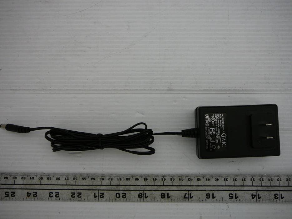
Click to zoom
Application Details
- Equipment Class
- DTS - Digital Transmission System
- Date of Grant
- Nov 29, 2010
- Application Purpose
- Original Equipment
- Date of Application
- Nov 29, 2010
- Equipment Note
- Wi-Fi and Bluetooth Developer Kit
- Frequency Range
- 2412.00000000 - 2462.00000000
- Company
- NVIDIA Corporation
- Country
- United States
Documents & Files
Document Text
Text extracted from the exhibit documents filed with the FCC. Open a document above to read the original.
Users Manual
- 1 - January 2010 NVIDIA Tegra 250 Developer Kit Hardware Introduction and Setup Version 100113.01 January 2010 - 2 - Contents INTRODUCTION 3 GETTING STARTED: OVERVIEW 4 UNBOXING 5 HOST PC CONFIGURATION 9 CONNECTING THE DEVKIT HW 9 “FLASHING” (INSTALLING) OPERATING SYSTEM IMAGES ONTO THE DEVKIT 12 USING YOUR BOOTED DEVKIT 18 CONNECTING THE MINI SATELLITE BOARD 19 January 2010 - 3 - Introduction This manual describes the basic, initial setup of an NVIDIA Tegra 250 developer kit (devkit), and is designed to assist a new user in understanding the hardware, selecting an operating system to install to the devkit, and connect and configure the hardware to boot that operating system. Very little operating system-specific information will be found in this manual, as each operating system supported by the Tegra 250 devkit includes its own support pack with software and documentation. This manual covers the details that tend to cross over all supported operating systems. What is “The Devkit”? The NVIDIA Tegra 250-based devkit is a compact, Smartbook-motherboard form factor computer-on-a-board with the following specifications: - Dual ARM Cortex A9 CPU @1GHz - 1GB of RAM - High-performance, shader-based 3D acceleration - HD video encode and decode - 512MB of Flash memory - Onboard wired Ethernet - WiFi - Bluetooth - Analog stereo audio in/out - USB keyboard/mouse/storage support - HDMI/DVI-D and VGA/CRT display support - Onboard SD(HC) slot January 2010 - 4 - Getting Started: Overview There are a few basic steps required to begin developing for the devkit: Unboxing: 1) Unpack the devkit components 2) Familiarize yourself with the components Host PC Configuration: 1) Select your desired devkit operating system 2) Download the support pack for that operating system from the NVIDIA Tegra developers website 3) Read the documentation provided with that support pack and install it to the appropriate host PC 4) Download and install any host PC support SW as required by the platform support pack’s documentation Connecting the Devkit HW: 1) Locate/procure the required hardware accessories for the devkit (somewhat dependent upon the selected devkit operating system image) 2) Select the desired video output based on your available display devices and the operating system image Installing the Operating System to the Devkit: 1) Follow the operating system image installation instructions provided with the support pack 2) Boot the devkit January 2010 - 5 - Unboxing Devkit Contents and Hardware Requirements As shipped, your devkit should contain the following items: • Devkit main board (rectangular circuit board containing the Tegra chip and connectors for networking, USB peripherals, storage and display devices) • 15V power adapter (USA 120V mains power connection) • Adjustable, folding, threaded WiFi antenna • Expansion board (smaller, square circuit board containing a serial port, LEDs and a few buttons) Also required to use the devkit, but not supplied (developer must provide these): • Host PC with USB ports. The exact OS that this host PC must be running may differ depending upon the devkit OS to be used, but is most frequently Microsoft Windows. • USB mini (NOT micro, as with previous Tegra devkits) to USB cable (for device setup and connectivity) • External display supporting VGA (15-pin D-Sub), HDMI or DVI (via HDMI-to-DVI adapter) • SD card or USB-based “thumb drive” for additional storage • USB mouse • USB keyboard Strongly recommended to use the devkit, but not supplied (developer should provide these): • Powered USB hub January 2010 - 6 - Getting Familiar with the Devkit Main Board The following diagram shows a Tegra 250 devkit main board with power connected. Important connectors are annotated: The annotated items include: • 15V Power jack. Supplies the main power to the devkit (the devkit as shipped to developers does not directly support battery power) • VGA (CRT) jack. Support for 15-pin D-Sub analog display output • HDMI jack. Support for digital display output • WiFi antenna jack. Connection point for supplied (or 3 rd -party) WiFi antenna • Tegra 250 chip. The heart and soul of the Tegra 250 devkit “ACOK” configuration switch Power LEDs Tegra chip WiFi Antenna jack 15V power jack HDMI jack Expansion board connectors Reset button Recovery button Power button USB-A jack VGA (CRT) jack Microphone jack Headphone jack SD Card slot Ethernet jack Dual USB- A jacks USB mini jack January 2010 - 7 - • USB-A jacks (3). Support for common peripherals (use of a powered USB hub is strongly recommended) • Expansion board connectors. “Header” connections for an expansion board (supplied) that adds status LEDs, copies of the power, reset and recovery buttons, and a serial port. • “ACOK” configuration switch. A configuration micro-switch that is used to adjust the power behavior of the devkit. In the left (BATT) position, the AC adapter simulates a battery, and the soft power button functions normally. In the right (NORM) position, applying power causes the device to turn on, without pressing the power button. The left (BATT) position is preferred for developers. • Power button. Pressing this switch will toggle the power to the device on and off • Recovery (flashing) button. Used to place the devkit in a special mode that leaves it ready to receive a new operating system image via USB (“recovery” mode) • Reset button. Soft reset • Microphone jack. Stereo microphone input as a 1/8” phone jack • Headphone jack. Stereo headphone output as a 1/8” phone jack • Ethernet jack. Wired networking if supported by the OS • SD card slot. Supports normal and high-capacity SD card storage • USB-mini jack. USB jack for flashing the device (updating OS images) and connecting the device to a host PC. January 2010 - 8 - Mini Satellite Board In addition, most Tegra 250 devkits include the “mini satellite board”, which replicates the main power, reset and recovery buttons, adds a UART serial port for low-level debugging on some OSes…
Text truncated - open the document above for the full version.
External Photos
Nvidia Corporation FCC ID: VOB-E1162, IC: 7361A-E1162 Report Number: R1003235-247WiFi Page 63 of 66 FCC Part 15C & IC RSS-210 Test Report 16 Exhibit C - EUT Photographs 16.1 EUT System View 16.2 EUT – Antenna View Nvidia Corporation FCC ID: VOB-E1162, IC: 7361A-E1162 Report Number: R1003235-247WiFi Page 64 of 66 FCC Part 15C & IC RSS-210 Test Report 16.3 EUT –AC/DC Adapter View
ID Label/Location Info
Nvidia Corporation FCC ID: VOB-E1162, IC: 7361A-E1162 Report Number: R1003235-247WiFi Page 58 of 66 FCC Part 15C & IC RSS-210 Test Report 14 Exhibit A - FCC & IC Equipment Labeling Requirements 14.1 FCC ID Label Requirements As per FCC §2.925, (a) Each equipment covered in an application for equipment authorization shall bear a nameplate or label listing the following: (1) FCC Identifier consisting of the two elements in the exact order specified in §2.926. The FCC Identifier shall be preceded by the term FCC ID in capital letters on a single line, and shall be of a type size large enough to be legible without the aid of magnification. Example: FCC ID: XXX123 Where: XXX—Grantee Code, 123—Equipment Product Code As per FCC §15.19, (a) In addition to the requirements in part 2 of this chapter, a device subject to certification, or verification shall be labeled as follows: (3) All other devices shall bear the following statement in a conspicuous location on the device: This device complies with part 15 of the FCC Rules. Operation is subject to the following two conditions: (1) This device may not cause harmful interference, and (2) this device must accept any interference received, including interference that may cause undesired operation. (4) Where a device is constructed in two or more sections connected by wires and marketed together, the statement specified above is required to be affixed only to the main control unit. If the EUT is integrated within another device then a label affixed to the host shall also state, “Contains FCC ID: XXXXXX” (5) When the device is so small or for such use that it is not practicable to place the statement specified under paragraph (a) of this section on it, the information required by this paragraph shall be placed in a prominent location in the instruction manual or pamphlet supplied to the user or, alternatively, shall be placed on the container in which the device is marketed. However, the FCC identifier or the unique identifier, as appropriate, must be displayed on the device. 14.2 IC Label Requirements As per IC RSS-Gen §5, the certification number shall appear as follows: IC: XXXXXX-YYYYYYYY Where: • "XXXXXX-YYYYYYYY" is the certification number • "XXXXXX" is the Certificate Holder Number (CHN), made of at most 6 alphanumeric characters (A-Z, 0-9), assigned by Industry Canada; and • "YYYYYYYY" is the Unique Product Number (UPN), made of at most 11 alphanumeric characters (A-Z, 0-9) assigned by the applicant. • Note 1: The term "IC" before the equipment certification number only signifies that the Industry Canada technical specifications were met. • Note 2: Note 1 shall be conspicuously placed in the equipment user manual. • Note 3: Permitted alphanumeric characters used in the CHN and UPN are limited to capital letters (A-Z) and digits (0-9). Other characters, such as "#", "/" or "-", shall not be used. Nvidia Corporation FCC ID: VOB-E1162, IC: 7361A-E1162 Report Number: R1003235-247WiFi Page 59 of 66 FCC Part 15C & IC RSS-210 Test Report As per IC RSS-Gen §5.2 Equipment Labeling: Equipment subject to certification under the applicable RSS, shall be permanently labeled on each item, or as an inseparable combination. The label must contain the following information for full compliance: (a) the certification number, prefixed by the term “IC:”; (b) the manufacturer's name, trade name or brand name; and (c) a model name or number. Equipment for which a certificate has been issued is not considered certified if it is not properly labeled. The information on the Canadian label can be combined with the manufacturer’s other labeling requirements. If the device size is too small to put a label, the label can be included in the user’s manual, upon agreement with Industry Canada. 14.3 Suggested FCC ID & IC Label 14.4 Suggested FCC ID & IC Label Location Model: E1162 This device complies with part 15 of the FCC Rules. Operation is subject to the following two conditions: (1) This device may not cause harmful interference, and (2) this device must accept any interference received, including interference that may cause undesired operation. FCC ID: VOB-E1162 IC: 7361A-E1162 Nvidia Corporation Label here
Internal Photos
Nvidia Corporation FCC ID: VOB-E1162, IC: 7361A-E1162 Report Number: R1003235-247WiFi Page 65 of 66 FCC Part 15C & IC RSS-210 Test Report 16.4 EUT – Board 1 Top View 16.5 EUT- Board 1 Rear View Nvidia Corporation FCC ID: VOB-E1162, IC: 7361A-E1162 Report Number: R1003235-247WiFi Page 66 of 66 FCC Part 15C & IC RSS-210 Test Report 16.6 EUT- Board 2Top View 16.7 EUT –Board 2 Rear View ***** END OF REPORT *****
RF Exposure Info
Nvidia Corporation FCC ID: VOB-E1162, IC: 7361A-E1162 Report Number: R1003235-247WiFi Page 10 of 66 FCC Part 15C & IC RSS-210 Test Report 4 FCC §15.247 (i), §2.1091 & IC & RSS-102 - RF Exposure Information 4.1 Applicable Standard According to FCC §15.247(i) and §1.1307(b)(1), systems operating under the provisions of this section shall be operated in a manner that ensures that the public is not exposed to radio frequency energy level in excess of the Commission’s guidelines. Limits for General Population/Uncontrolled Exposure Frequency Range (MHz) Electric Field Strength (V/m) Magnetic Field Strength (A/m) Power Density (mW/cm 2 ) Averaging Time (minutes) Limits for General Population/Uncontrolled Exposure 0.3-1.34 614 1.63 *(100) 30 1.34-30 824/f 2.19/f *(180/f 2 ) 30 30-300 27.5 0.073 0.2 30 300-1500 / / f/1500 30 1500-100,000 / / 1.0 30 f = frequency in MHz * = Plane-wave equivalent power density Before equipment certification is granted, the procedure of IC RSS-102 must be followed concerning the exposure of humans to RF fields. According to RSS-102 Issue 2 section 4.1, RF limits used for general public will be applied to the EUT. Frequency Range (MHz) Electric Field (V/m rms) Magnetic Field (A/m rms) Power Density (W/m 2 ) Time Averaging (min) 0.003 - 1 280 2.19 - 6 1 - 10 280 / f 2.19 / f - 6 10 - 30 28 2.19 / f - 6 30 – 300 28 0.073 2* 6 300 – 1 500 1.585 f 0.5 0.0042 f 0.5 f / 150 6 1 500 – 15 000 61.4 0.163 10 6 15 000 – 150 000 61.4 0.163 10 616000 / f 1.2 150 000- 300 000 0.158 f 0.5 4.21 x 10 -4 f 0.5 6.67 x 10 -5 f 616000 / f 1.2 Note: ƒ is frequency in MHz * Power density limit is applicable at frequencies greater than 100 MHz Nvidia Corporation FCC ID: VOB-E1162, IC: 7361A-E1162 Report Number: R1003235-247WiFi Page 11 of 66 FCC Part 15C & IC RSS-210 Test Report 4.2 MPE Prediction Predication of MPE limit at a given distance, Equation from OET Bulletin 65, Edition 97-01 S = PG/4πR² Where: S = power density P = power input to antenna G = power gain of the antenna in the direction of interest relative to an isotropic radiator R = distance to the center of radiation of the antenna 4.3 MPE Results Maximum peak output power at antenna input terminal (dBm):15.43 Maximum peak output power at antenna input terminal (mW): 34.914 Prediction distance (cm): 20 Prediction frequency (MHz): 2437 Maximum Antenna Gain, typical (dBi): 2.0 Maximum Antenna Gain (numeric): 1.585 Power density of prediction frequency at 20.0 cm (mW/cm 2 ): 0.011 Power density of prediction frequency at 20.0 cm (W/m 2 ): 0.11 MPE limit for uncontrolled exposure at prediction frequency (mW/cm 2 ): 1.0 MPE limit for uncontrolled exposure at prediction frequency (W/m 2 ):10 The device is compliant with the requirement MPE limit for uncontrolled exposure. The maximum power density at the distance of 20 cm is 0.011 mW/cm 2 (0.11 W/m 2 ).Limit is 1 mW/cm 2 (10 W/m 2 ).
Test Report
Note: This test report is prepared for the customer shown above and for the device described herein. It may not be duplicated or used in part without prior written consent from Bay Area Compliance Laboratories Corp. This report must not be used by the customer to claim product certification, approval, or endorsement by NVLAP*, NIST, or any agency of the Federal Government. * This report may contain data that are not covered by the NVLAP accreditation and are marked with an asterisk “*” (Rev.2) FCC PART 15C IC RSS-210 ISSUE 7, JUNE 2007 TEST AND MEASUREMENT REPORT For Nvidia Corporation 2701 San Tomas Expressway, Santa Clara, CA 95050, USA FCC ID: VOB-E1162 IC: 7361A-E1162 Report Type: Original Report Product Type: Developer Kit with embedded Wi-Fi and BT Test Engineer: Jack Liu Report Number: R1003235-247WiFi Report Date: 2010-11-01 Reviewed By: Victor Zhang RF Lead Prepared By: (84) Bay Area Compliance Laboratories Corp. 1274 Anvilwood Avenue, Sunnyvale, CA 94089, USA Tel: (408) 732-9162 Fax: (408) 732 9164 Nvidia Corporation FCC ID: VOB-E1162, IC: 7361A-E1162 Report Number: R1003235-247WiFi Page 2 of 66 FCC Part 15C & IC RSS-210 Test Report TABLE OF CONTENTS 1 General Description .................................................................................................................................................... 5 1.1 Product Description for Equipment Under Test (EUT) ....................................................................................... 5 1.2 Mechanical Description of EUT .......................................................................................................................... 5 1.3 Objective.............................................................................................................................................................. 5 1.4 Related Submittal(s)/Grant(s) .............................................................................................................................. 5 1.5 Test Methodology................................................................................................................................................ 5 1.6 Measurement Uncertainty.................................................................................................................................... 5 1.7 Test Facility......................................................................................................................................................... 6 2 System Test Configuration ......................................................................................................................................... 7 2.1 Justification.......................................................................................................................................................... 7 2.2 EUT Exercise Software ....................................................................................................................................... 7 2.3 Equipment Modifications .................................................................................................................................... 7 2.4 Special Accessories ............................................................................................................................................. 7 2.5 Local Support Equipment .................................................................................................................................... 7 2.6 Power Supply and Line Filters............................................................................................................................. 7 2.7 Interface Ports and Cabling ................................................................................................................................. 7 2.8 Internal Parts List and Details.............................................................................................................................. 8 3 Summary of Test Results ............................................................................................................................................ 9 4 FCC §15.247 (i), §2.1091 & IC & RSS-102 - RF Exposure Information ................................................................ 10 4.1 Applicable Standard .......................................................................................................................................... 10 4.2 MPE Prediction.................................................................................................................................................. 11 4.3 MPE Results ...................................................................................................................................................... 11 5 FCC §15.203 & IC RSS-Gen §7.1.4 – ANTENNA REQUIREMENT .................................................................... 12 5.1 Applicable Standard .......................................................................................................................................... 12 5.2 Result ................................................................................................................................................................. 12 6 FCC §15.207 & RSS-Gen 7.2.2- Conducted Emissions ............................................................................................ 13 6.1 Applicable Standards ......................................................................................................................................... 13 6.2 Test Setup .......................................................................................................................................................... 13 6.3 Test Equipment List and Details........................................................................................................................ 13 6.4 Test Setup Block Diagram................................................................…
Text truncated - open the document above for the full version.
Test Setup Photos
Nvidia Corporation FCC ID: VOB-E1162, IC: 7361A-E1162 Report Number: R1003235-247WiFi Page 60 of 66 FCC Part 15C & IC RSS-210 Test Report 15 Exhibit B - Test Setup Photographs 15.1 Radiated Emission below 1 GHz Front View 15.2 Radiated Emission below 1 GHz Rear View Nvidia Corporation FCC ID: VOB-E1162, IC: 7361A-E1162 Report Number: R1003235-247WiFi Page 61 of 66 FCC Part 15C & IC RSS-210 Test Report 15.3 Radiated Emission above 1 GHz Front View 15.4 Radiated Emission above 1 GHz Front View Nvidia Corporation FCC ID: VOB-E1162, IC: 7361A-E1162 Report Number: R1003235-247WiFi Page 62 of 66 FCC Part 15C & IC RSS-210 Test Report 15.5 AC Line Conducted Emission Front View 15.6 AC Line Conducted Emission Side View
Contact Information
Applicant
Charles Jackson
Test Firm
Bay Area Compliance LaboratoryJohn Chan
Technical Specifications
| # | Rule Parts | Frequency Range | Power Output |
|---|---|---|---|
| 2 | 15C | 2.41 GHz - 2.46 GHz | 32.00 mW |
Other Applications from NVIDIA Corporation
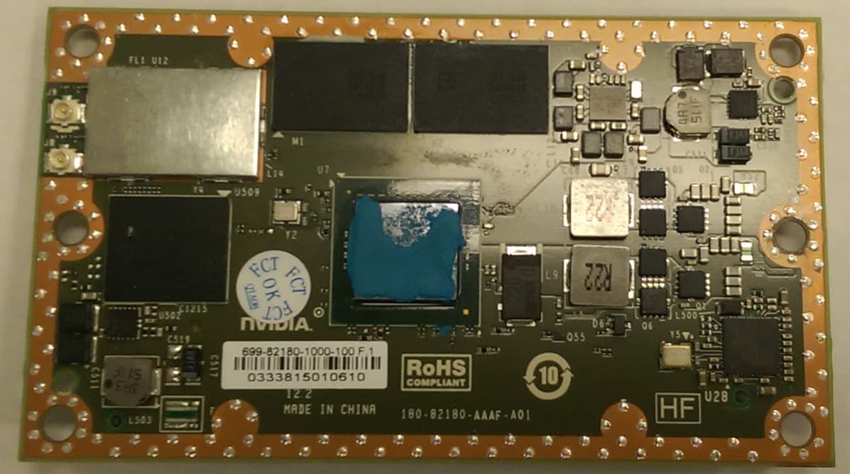
VOB-P2180
Nov 04, 2015WLAN 2X2 MIMO 802.11a/b/g/n/ac with Bluetooth
Equipment Class
DSS - Part 15 Spread Spectrum Transmitter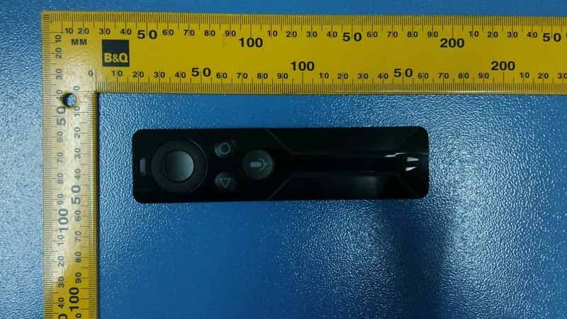
VOB-P2575
Apr 08, 2015Remote Control
Equipment Class
DSS - Part 15 Spread Spectrum Transmitter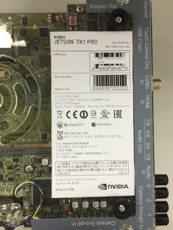
VOB-P1860
Apr 01, 2015Development Platform
Equipment Class
NII - Unlicensed National Information Infrastructure TX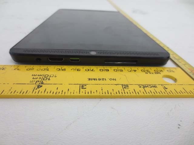
VOB-P1761WX
Mar 15, 2015Tablet
Equipment Class
DTS - Digital Transmission System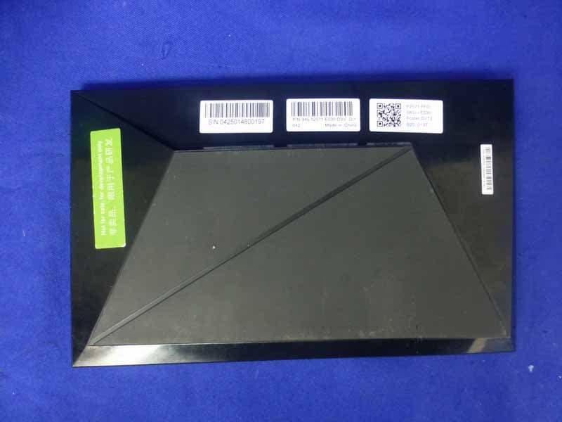
VOB-P2571
Mar 11, 2015Complex Set-Top Box
Equipment Class
DTS - Digital Transmission System