VOB-P1860Development Platform
NVIDIA Corporation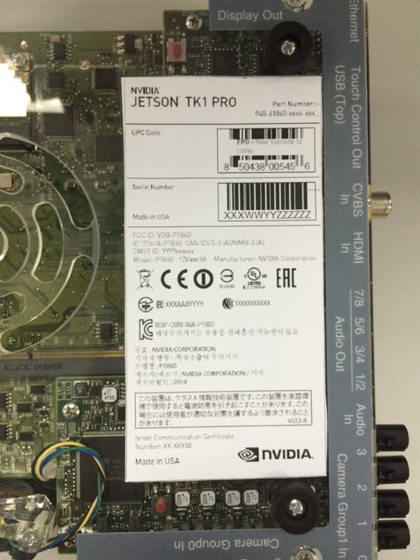
Click to zoom
Application Details
- Equipment Class
- NII - Unlicensed National Information Infrastructure TX
- Date of Grant
- Apr 01, 2015
- Application Purpose
- Original Equipment
- Date of Application
- Mar 30, 2015
- Equipment Note
- Development Platform
- Frequency Range
- 5745.00000000 - 5825.00000000
- Company
- NVIDIA Corporation
- Country
- United States
Documents & Files
Document Text
Text extracted from the exhibit documents filed with the FCC. Open a document above to read the original.
Users Manual
NVIDIA Jetson TK1 Pro User Manual Before you start This document is intended to cover the Hardware aspects of the Jetson TK1 Pro Development Kit. The document covers how to bring the board up for the first time – and includes information about all the available interfaces on the platform (including header connectors). Tip: Please refer to the documentation provided with the Android package that comes with the Jetson TK1 Pro Development Kit for more details regarding the software options on the platform. Assumptions This document assumes you have received a Jetson TK1 Pro Development Kit from NVIDIA with a pre- installed Android OS. If this is not the case, please contact your NVIDIA representative. Hardware You should have received the following items with your Jetson TK1 Pro Platform as depicted in Error! Reference source not found.: • Jetson TK1 Pro Platform which consists of: o Jetson TK1 Pro Main Board (P1860) o Tegra VCM board (connected to the main board – top) (P1859) o Embedded Breakout Board (connected to the main board – bottom) (P1892) o Touch Screen Display (P1332) • Power Supply • 3 Antennas (Wi-Fi, Bluetooth and GPS) • USB cable (mini-USB to USB) • mDP cable • Cable for Touch Screen (Touch and Power) Minimum Hardware Setup The minimum requirements to bring the system up are: • Power Supply • Touch Screen Display or HDMI monitor(not provided) o mDP and Tyco cables (are required for the Touch Screen configuration) o HDMI cable(not provided) can be used for HDMI monitor instead of Touch Screen • USB Keyboard and Mouse (not provided) but strongly recommended While the Jetson TK1 Pro platform supports multiple configurations and its modular approach provides flexibility, the section below focuses on bringing the platform up for the first time with the minimum configuration effort required. Connections need to be done to: the Main board (P1860), the EBB board (P1892) and Touch Screen (P1332). Main Board (P1860) Minimum Connections Figure 1 shows all the main board component with labels. Bottom: Top: Figure 1: Mainboard with Component Labels The following connections need to be made on the main board (P1860) as a minimum in order to boot Jetson TK1 Pro for the first time: Power Supply (J14): Power supply can be connected to the connector labeled J14 as shown on Error! Reference source not found.. mDP Connector (J9): Using the mDP cable provided, the board needs to be connected to the Touch Screen Display included in the package. Main Board (P1860) Optional Connections The following connections are not required for the board to boot. USB Mouse and Keyboard (J2&J3): While this is optional, is highly recommended that a USB mouse and keyboard are plugged-in in to the platform via the main board J2 connector. HDMI Connector (J8): This is only required if the Touch Screen provided with the platform will not be used. USB Connection (J35): The USB cable provided with the Jetson TK1 Pro platform while is not required to boot it is recommended to be connected to mini-USB connector labeled “Host PC USB (Console)” on the Jetson TK1 Pro board and to a USB 2.0 port on the workstation running Ubuntu Linux 12.04. The “Host PC USB (Console)” port is labeled J4 on Figure 1. The USB connection enables debug and development capabilities. Please refer to the.CHM documentation file for more details on how to configure this capability. Ethernet Connection (J1000): While the Ethernet port connection is optional – and may require further configuration not covered on this document – to gain network access, an Ethernet cable can be connected to the port labeled J1000 on Figure 1. EBB Board (P1892) Minimum Connections Error! Reference source not found. shows all the EBB board component with labels. Please be aware that some connectors - while accessible on the side of the board - their labels are not visible as are placed on the other side of the EBB board. Please refer to Figure 3 for details on these connectors. Bottom: Top: Figure 3: EBB board with Component Labels The following connections need to be made on the main board (P1892) as a minimum in order to boot Jetson TK1 Pro for the first time (assuming the Touch Panel Display is utilized): Touch Screen Connector (J23): Using the Tyco cable provided, the board needs to be connected to the display as well. If the Touch Panel Display will not be utilized a HDMI monitor can be used instead. RF module Jetson TK1 Pro comes equipped with a Wi-Fi/BT/GPS module (labeled J6 on Figure 1). The board is shipped with 3 different antennas that need to be connected to J6. The Communication Module (J6) has four different connectors as depicted on Figure . Figure 4: Communication Module (J6) - Antenna Connectors . Antenna (Part Number) Connects on: 311-0046-000 (2.4GHz – Wi-Fi Main / Bluetooth) P1 311-0045-000 (5GHz –Wi-Fi Aux) P2 311-0047-000 (GPS) P4 Table 1: Antenna Mapping of Communication Module (J6) The antennas shall be connected as described on Table 1. Jetson TK1 Pro Hardware Architecture The Jetson TK1 Pro board architecture is depicted on Figure below. The modular architecture allows maximum flexibility and custom configurations. Figure 5: Jetson TK1 Pro Hardware Architecture It is important to highlight the use of SMSC’s 9514 in order to simplify the connection to the Jetson TK1 Pro Platform. With this approach only a USB connection is needed (via J4) in order to have a serial console, network connectivity to the board (i.e. NFS drive mounting, etc.) and reflashing of the system. Boot up Step 1, Connect the touch panel to the P1860 main platform. The miniDP cable should plug into the VCM DP port. Main platform side: Figure 6 Touch panel side: Figure 7 Step 2, plug the AC-DC adaptor into the Power In #1 port and turn on the power switch. Figure 8 Step 3, done. Figure 9: Jetson TK1 Pro up and running Compliance The P1860 is compliant with the regulations listed in this section. United States Federal Communications Commission (FCC) FCC ID: VOB-P1860 This device …
Text truncated - open the document above for the full version.
External Photos
1 Photographs - EUT Constructional Details Test model No.: P1860
ID Label/Location Info
940-61860-xxxx-xxx 8 50438 00545 6 FCC ID: VOB-P1860 IC: 7361A-P1860 CAN ICES-3 (A)/NMB-3 (A) CMIIT ID: YYYYxxxxxx Model: P1860 MSIP-CMM-NVA-P1860 : NVIDIA CORPORATION : : P1860 / : NVIDIA CORPORATION / : 2014 XXXAAAYYYY Israel Communication Certificate Number: XX-XXXXX U L US C LISTED XXXXXXXXXXX Made in USA JETSON TK1 PRO Made in USA A VCCI-A FPO - New barcode to come XXXWWYYZZZZZZ 2.5” 12V 5A Manufacturer: NVIDIA Corporation
Internal Photos
1 Photographs - EUT Constructional Details Test model No.: P1860
RF Exposure Info
SGS-CSTC Standards Technical Services Co., Ltd. No. 1 Workshop, M-10, Middle section, Science & Technology Park, Nanshan District, Shenzhen, Guangdong, China 518057 Telephone: +86 (0) 755 2601 2053 Fax: +86 (0) 755 2671 0594 Email: [email protected] Report No.: SZEM141100618206 Page: 1 of 9 Authorized Signature: Jack Zhang EMC Laboratory Manager The manufacturer should ensure that all products in series production are in conformity with the product sample detailed in this report. If the product in this report is used in any configuration other than that detailed in the report, the manufacturer must ensure the new system complies with all relevant standards. Any mention of SGS International Electrical Approvals or testing done by SGS International Electrical Approvals in connection with, distribution or use of the product described in this report must be approved by SGS International Electrical Approvals in writing. The report must not be used by the client to claim product certification, approval, or endorsement by NVLAP, NIST, or any agency of the federal government. All test results in this report can be traceable to National or International Standards. “This document is issued by the Company subject to its General Conditions of Service printed overleaf, available on request or accessible at www.sgs.com/terms_and_conditions.htm and, for electronic format documents, subject to Terms and Conditions for Electronic Documents at www.sgs.com/terms_e-document.htm. Attention is drawn to the limitation of liability, indemnification and jurisdiction issues defined therein. Any holder of this document is advised that information contained hereon reflects the Company’s findings at the time of its intervention only and within the limits of Client’s instructions, if any. The Company’s sole responsibility is to its Client and this document does not exonerate parties to a transaction from exercising all their rights and obligations under the transaction documents. This document cannot be reproduced except in full, without prior written approval of the Company. Any unauthorized alteration, forgery or falsification of the content or appearance of this document is unlawful and offenders may be prosecuted to the fullest extent of the law. Unless otherwise stated the results shown in this test report refer only to the sample(s) tested and such sample(s) are retained for 90 days only.” 1 Cover page RF Exposure Evaluation Report Application No.: SZEM1411006182CR Applicant: NVIDIA Corporation Manufacturer: NVIDIA Corporation Factory MEGAFORCE CORP Product Name: Development Platform Model No.(EUT): P1860 Trade Mark: NVIDIA FCC ID: VOB-P1860 Standards: 47 CFR Part 1.1307 (2014) 47 CFR Part 1.1310 (2014) Date of Receipt: 2014-11-13 Date of Test: 2015-02-09 to 2015-02-15 Date of Issue: 2015-03-25 Test Result : PASS* * In the configuration tested, the EUT complied with the standards specified above. SGS-CSTC Standards Technical Services Co., Ltd. Report No.: SZEM141100618206 Page: 2 of 9 “This document is issued by the Company subject to its General Conditions of Service printed overleaf, available on request or accessible at www.sgs.com/terms_and_conditions.htm and, for electronic format documents, subject to Terms and Conditions for Electronic Documents at www.sgs.com/terms_e-document.htm. Attention is drawn to the limitation of liability, indemnification and jurisdiction issues defined therein. Any holder of this document is advised that information contained hereon reflects the Company’s findings at the time of its intervention only and within the limits of Client’s instructions, if any. The Company’s sole responsibility is to its Client and this document does not exonerate parties to a transaction from exercising all their rights and obligations under the transaction documents. This document cannot be reproduced except in full, without prior written approval of the Company. Any unauthorized alteration, forgery or falsification of the content or appearance of this document is unlawful and offenders may be prosecuted to the fullest extent of the law. Unless otherwise stated the results shown in this test report refer only to the sample(s) tested and such sample(s) are retained for 90 days only.” 2 Version Revision Record Version Chapter Date Modifier Remark 00 2015-03-25 Original Authorized for issue by: Tested By 2015-02-15 (Chris Zhong) /Project Engineer Date Prepared By 2015-03-25 (Vivi Zhou) /Clerk Date Checked By 2015-03-25 (Owen Zhou) /Reviewer Date SGS-CSTC Standards Technical Services Co., Ltd. Report No.: SZEM141100618206 Page: 3 of 9 “This document is issued by the Company subject to its General Conditions of Service printed overleaf, available on request or accessible at www.sgs.com/terms_and_conditions.htm and, for electronic format documents, subject to Terms and Conditions for Electronic Documents at www.sgs.com/terms_e-document.htm. Attention is drawn to the limitation of liability, indemnification and jurisdiction issues defined therein. Any holder of this document is advised that information contained hereon reflects the Company’s findings at the time of its intervention only and within the limits of Client’s instructions, if any. The Company’s sole responsibility is to its Client and this document does not exonerate parties to a transaction from exercising all their rights and obligations under the transaction documents. This document cannot be reproduced except in full, without prior written approval of the Company. Any unauthorized alteration, forgery or falsification of the content or appearance of this document is unlawful and offenders may be prosecuted to the fullest extent of the law. Unless otherwise stated the results shown in this test report refer only to the sample(s) tested and such sample(s) are retained for 90 days only.” 3 Contents Page 1 COVER PAGE ................................................................................................................................…
Text truncated - open the document above for the full version.
Test Report
SGS-CSTC Standards Technical Services Ltd. No. 1 Workshop, M-10, Middle section, Science & Technology Park, Nanshan District, Shenzhen, Guangdong, China 518057 Telephone: +86 (0) 755 2601 2053 Fax: +86 (0) 755 2671 0594 Email: [email protected] Report No.: SZEM141100618205 Page: 1 of 52 Authorized Signature: Jack Zhang EMC Laboratory Manager The manufacturer should ensure that all products in series production are in conformity with the product sample detailed in this report. If the product in this report is used in any configuration other than that detailed in the report, the manufacturer must ensure the new system complies with all relevant standards. Any mention of SGS International Electrical Approvals or testing done by SGS International Electrical Approvals in connection with, distribution or use of the product described in this report must be approved by SGS International Electrical Approvals in writing. The report must not be used by the client to claim product certification, approval, or endorsement by NVLAP, NIST, or any agency of the federal government. All test results in this report can be traceable to National or International Standards. “This document is issued by the Company subject to its General Conditions of Service printed overleaf, available on request or accessible at www.sgs.com/terms_and_conditions.htm and, for electronic format documents, subject to Terms and Conditions for Electronic Documents at www.sgs.com/terms_e-document.htm. Attention is drawn to the limitation of liability, indemnification and jurisdiction issues defined therein. Any holder of this document is advised that information contained hereon reflects the Company’s findings at the time of its intervention only and within the limits of Client’s instructions, if any. The Company’s sole responsibility is to its Client and this document does not exonerate parties to a transaction from exercising all their rights and obligations under the transaction documents. This document cannot be reproduced except in full, without prior written approval of the Company. Any unauthorized alteration, forgery or falsification of the content or appearance of this document is unlawful and offenders may be prosecuted to the fullest extent of the law. Unless otherwise stated the results shown in this test report refer only to the sample(s) tested and such sample(s) are retained for 90 days only.” 1 Cover page FCC REPORT Application No: SZEM1411006182CR Applicant: NVIDIA Corporation Manufacturer: NVIDIA Corporation Factory: MEGAFORCE CORP Product Name: Development Platform Model No.(EUT): P1860 Trade Mark: NVIDIA FCC ID: VOB-P1860 Standards: 47 CFR Part 15, Subpart E (2014) Date of Receipt: 2014-11-13 Date of Test: 2015-02-09 to 2015-02-15 Date of Issue: 2015-03-25 Test Result: PASS * . * In the configuration tested, the EUT complied with the standards specified above. SGS-CSTC Standards Technical Services Ltd. Report No.: SZEM141100618205 Page: 2 of 52 “This document is issued by the Company subject to its General Conditions of Service printed overleaf, available on request or accessible at www.sgs.com/terms_and_conditions.htm and, for electronic format documents, subject to Terms and Conditions for Electronic Documents at www.sgs.com/terms_e-document.htm. Attention is drawn to the limitation of liability, indemnification and jurisdiction issues defined therein. Any holder of this document is advised that information contained hereon reflects the Company’s findings at the time of its intervention only and within the limits of Client’s instructions, if any. The Company’s sole responsibility is to its Client and this document does not exonerate parties to a transaction from exercising all their rights and obligations under the transaction documents. This document cannot be reproduced except in full, without prior written approval of the Company. Any unauthorized alteration, forgery or falsification of the content or appearance of this document is unlawful and offenders may be prosecuted to the fullest extent of the law. Unless otherwise stated the results shown in this test report refer only to the sample(s) tested and such sample(s) are retained for 90 days only.” 2 Version Revision Record Version Chapter Date Modifier Remark 00 2015-03-25 Original Authorized for issue by: Tested By 2015-02-15 (Chris Zhong) /Project Engineer Date Prepared By 2015-03-25 (Vivi Zhou) /Clerk Date Checked By 2015-03-25 (Owen Zhou) /Reviewer Date SGS-CSTC Standards Technical Services Ltd. Report No.: SZEM141100618205 Page: 3 of 52 “This document is issued by the Company subject to its General Conditions of Service printed overleaf, available on request or accessible at www.sgs.com/terms_and_conditions.htm and, for electronic format documents, subject to Terms and Conditions for Electronic Documents at www.sgs.com/terms_e-document.htm. Attention is drawn to the limitation of liability, indemnification and jurisdiction issues defined therein. Any holder of this document is advised that information contained hereon reflects the Company’s findings at the time of its intervention only and within the limits of Client’s instructions, if any. The Company’s sole responsibility is to its Client and this document does not exonerate parties to a transaction from exercising all their rights and obligations under the transaction documents. This document cannot be reproduced except in full, without prior written approval of the Company. Any unauthorized alteration, forgery or falsification of the content or appearance of this document is unlawful and offenders may be prosecuted to the fullest extent of the law. Unless otherwise stated the results shown in this test report refer only to the sample(s) tested and such sample(s) are retained for 90 days only.” 3 Test Summary Test Item Test Requirement Test method Result Antenna Requirement 47 CFR Part 15 Section 15.203 ANSI C63.10: 2009 PASS AC Power Line Conducted Emission 47 CFR Part 15 Section 15.207 ANSI C63…
Text truncated - open the document above for the full version.
Test Setup Photos
1 P H O T O G R AP H S Test model No.: P1860 1. 1 CO N D U C TE D EM I S S I O N TE S T SE TU P Front View Left View Right view 1. 2 RAD I AT E D DI S T U R B AN C E(30M HZ-1GHZ) TE S T SE TU P Front view Back view Left view 1. 3 RAD I AT E D DI S T U R B AN C E(AB O V E 1GHZ) TE S T SE T U P Front view Back view Left view Right view
Contact Information
Applicant
Charles Jackson
Technical Contact
SGS-CSTC Standards Technical ServicesLtdLi Emen
[email protected]0755-2654 4119
No.1 Workshop, M-10, Middle Section, · Shenzhen · China
Test Firm
SGS-CSTC Standards Technical Services Co.,Ltd.June Zhang
Technical Specifications
| # | Rule Parts | Frequency Range | Power Output |
|---|---|---|---|
| 2 | 15E | 5.75 GHz - 5.83 GHz | 4.00 mW |
Other Applications from NVIDIA Corporation
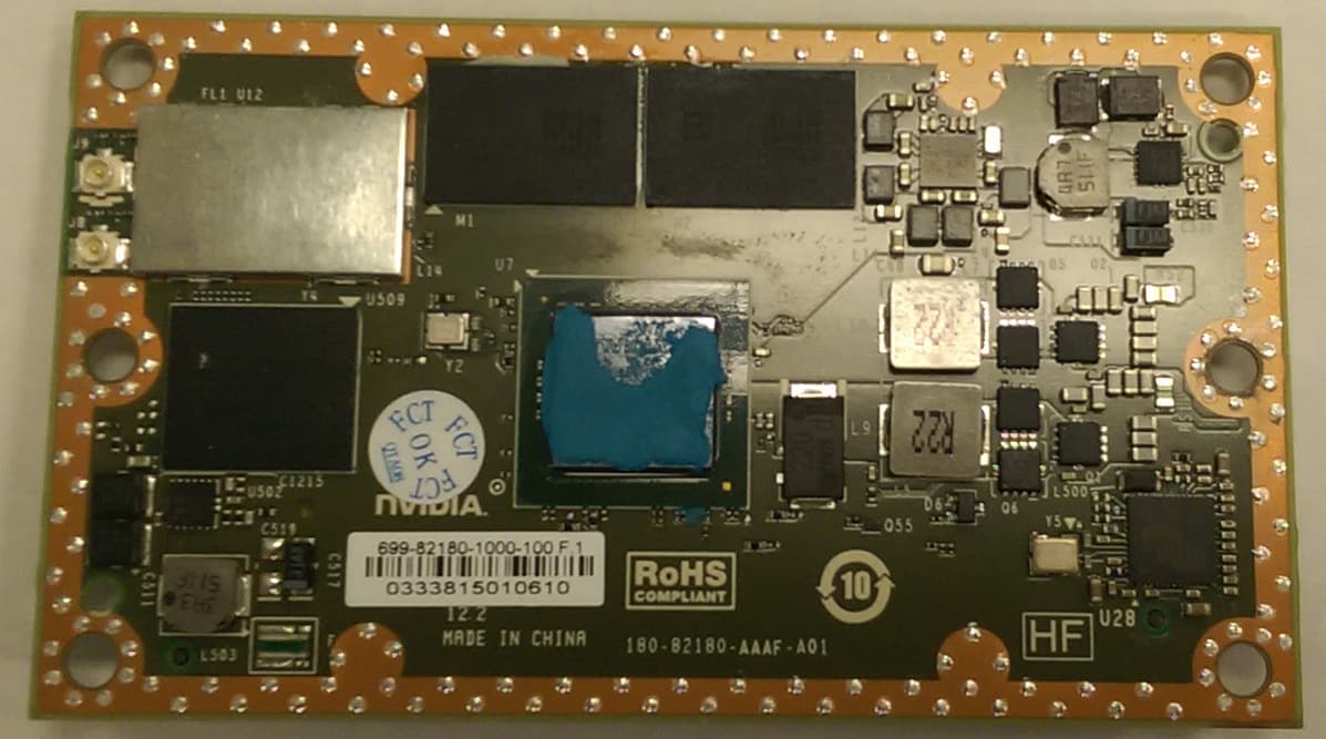
VOB-P2180
Nov 04, 2015WLAN 2X2 MIMO 802.11a/b/g/n/ac with Bluetooth
Equipment Class
DSS - Part 15 Spread Spectrum Transmitter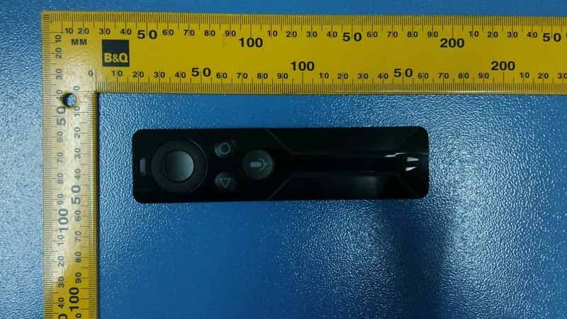
VOB-P2575
Apr 08, 2015Remote Control
Equipment Class
DSS - Part 15 Spread Spectrum Transmitter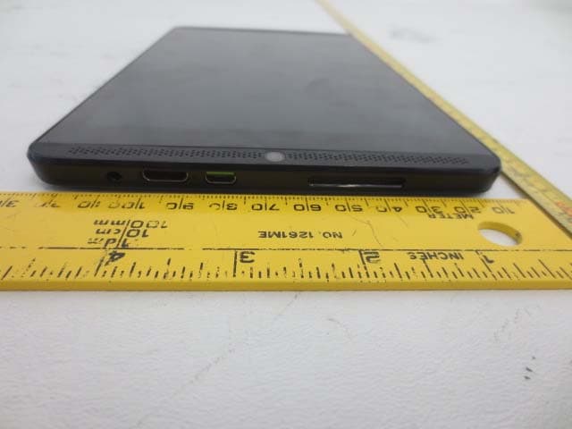
VOB-P1761WX
Mar 15, 2015Tablet
Equipment Class
DTS - Digital Transmission System
VOB-P2571
Mar 11, 2015Complex Set-Top Box
Equipment Class
DTS - Digital Transmission System
VOB-P1761W
Jun 15, 2014Tegra K1 Tablet
Equipment Class
DSS - Part 15 Spread Spectrum Transmitter