VOB-P2180WLAN 2X2 MIMO 802.11a/b/g/n/ac with Bluetooth
NVIDIA Corporation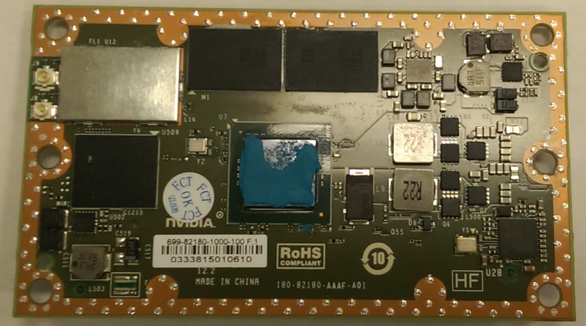
Click to zoom
Application Details
- Equipment Class
- DSS - Part 15 Spread Spectrum Transmitter
- Date of Grant
- Nov 04, 2015
- Application Purpose
- Original Equipment
- Date of Application
- Nov 03, 2015
- Equipment Note
- WLAN 2X2 MIMO 802.11a/b/g/n/ac with Bluetooth
- Frequency Range
- 2402.00000000 - 2480.00000000
- Company
- NVIDIA Corporation
- Country
- United States
Documents & Files
Document Text
Text extracted from the exhibit documents filed with the FCC. Open a document above to read the original.
Users Manual
Regulatory Module Integration Instructions This module has been granted modular approval for mobile applications. OEM integrators for host products may use the module in their final products without additional FCC / IC (Industry Canada) certification if they meet the following conditions. Otherwise, additional FCC / IC approvals must be obtained. The host product with the module installed must be evaluated for simultaneous transmission requirements. The users manual for the host product must clearly indicate the operating requirements and conditions that must be observed to ensure compliance with current FCC / IC RF exposure guidelines. To comply with FCC / IC regulations limiting both maximum RF output power and human exposure to RF radiation, the maximum antenna gain including cable loss in a mobile- only exposure condition must not exceed the following: Peak Antenna Gain Antenna Cable Loss Any device incorporating this module must include an external, visible, permanent marking or label which states: Contains FCC ID: VOB-P2180 Contains IC: 7361A-P2180 The final host / module combination may also need to be evaluated against the FCC Part 15B criteria for unintentional radiators in order to be properly authorized for operation as a Part 15 digital device. If the final host / module combination is intended for use as a portable device (see classifications below) the host manufacturer is responsible for separate approvals for the SAR requirements from FCC Part 2.1093 and RSS-102. Note: In the case where the Host / Module combination has been re-certified the FCC ID shall appear in the product manual. Device Classifications Since host devices vary widely with design features and configurations module integrators shall follow the guidelines below regarding device classification and simultaneous transmission, and seek guidance from their preferred regulatory test lab to determine how regulatory guidelines will impact the device compliance. Proactive management of the regulatory process will minimize unexpected schedule delays and costs due to unplanned testing activities. The module integrator must determine the minimum distance required between their host device and the user’s body. The FCC provides device classification definitions to assist in making the correct determination. Note that these classifications are guidelines only; strict adherence to a device classification may not satisfy the regulatory requirement as near-body device design details may vary widely. Your preferred test lab will be able to assist in determining the appropriate device category for your host product and if a KDB or PBA must be submitted to the FCC. Note, the module you are using has been granted modular approval for mobile applications. Portable applications may require further RF exposure (SAR) evaluations. It is also likely that the host / module combination will need to undergo testing for FCC Part 15 regardless of the device classification. Your preferred test lab will be able to assist in determining the exact tests which are required on the host / module combination. It is the responsibility of the manufacturer of the final product to verify whether or not further standards, recommendations or directives are in force FCC Definitions Portable: (§2.1093) — A portable device is defined as a transmitting device designed to be used so that the radiating structure(s) of the device is / are within 20 centimeters of the body of the user. Mobile: (§2.1091) (b) — A mobile device is defined as a transmitting device designed to be used in other than fixed locations and to generally be used in such a way that a separation distance of at least 20 centimeters is normally maintained between the transmitter’s radiating structure(s) and the body of the user or nearby persons. Per §2.1091d(d)(4) In some cases (for example, modular or desktop transmitters), the potential conditions of use of a device may not allow easy classification of that device as either Mobile or Portable. In these cases, applicants are responsible for determining minimum distances for compliance for the intended use and installation of the device based on evaluation of either specific absorption rate (SAR), field strength, or power density, whichever is most appropriate. Simultaneous Transmission Evaluation Any simultaneous transmission condition established through module integration into a host product must be evaluated per the requirements in KDB447498 and KDB616217 (for laptop, notebook, netbook, and tablet applications). These requirements include, but are not limited to: Transmitters and modules certified for mobile or portable exposure conditions can be incorporated in mobile host devices without further testing or certification when: The closest separation among all simultaneous transmitting antennas is >20 cm, Or Antenna separation distance and MPE compliance requirements for ALL simultaneous transmitting antennas have been specified in the application filing of at least one of the certified transmitters within the host device. In addition, when transmitters certified for portable use are incorporated in a mobile host device, the antenna(s) must be >5 cm from all other simultaneous transmitting antennas. All antennas in the final product must be at least 20 cm from users and nearby persons. OEM Instruction Manual Content Consistent with §2.909(a), the following text must be included within the user’s manual or operator instruction guide for the final commercial product. OEM-specific content is displayed in bold-italics. Operating Requirements and Conditions: The design of (Product Name) complies with U.S. Federal Communications Commission (FCC) guidelines respecting safety levels of radio frequency (RF) exposure for (OEM manufacturer to insert device classification: Mobile or Portable) devices. FCC ID: This product contains FCC ID: (Include FCCID of the Module) Note: In the case where the Host / Module combination has been re…
Text truncated - open the document above for the full version.
Users Manual
NVIDIA Corporation | 2701 San Tomas Expressway | Santa Clara, CA 95050 | +1 408 486-2000 | www.nvidia.com Jetson TX1 Developer Kit User Guide October 2015 Notice ALL NVIDIA DESIGN SPECIFICATIONS, REFERENCE BOARDS, FILES, DRAWINGS, DIAGNOSTICS, LISTS, AND OTHER DOCUMENTS (TOGETHER AND SEPARATELY, "MATERIALS") ARE BEING PROVIDED "AS IS." NVIDIA MAKES NO WARRANTIES, EXPRESS, IMPLIED, STATUTORY, OR OTHERWISE WITH RESPECT TO THE MATERIALS, AND ALL EXPRESS OR IMPLIED CONDITIONS, REPRESENTATIONS AND WARRANTIES, INCLUDING ANY IMPLIED WARRANTY OR CONDITION OF TITLE, MERCHANTABILITY, SATISFACTORY QUALITY, FITNESS FOR A PARTICULAR PURPOSE AND ON-INFRINGEMENT, ARE HEREBY EXCLUDED TO THE MAXIMUM EXTENT PERMITTED BY LAW. Information furnished is believed to be accurate and reliable. However, NVIDIA Corporation assumes no responsibility for the consequences of use of such information or for any infringement of patents or other rights of third parties that may result from its use. No license is granted by implication or otherwise under any patent or patent rights of NVIDIA Corporation. Specifications mentioned in this publication are subject to change without notice. This publication supersedes and replaces all information previously supplied. NVIDIA Corporation products are not authorized for use as critical components in life support devices or systems without express written approval of NVIDIA Corporation. Trademarks NVIDIA, the NVIDIA logo and Tegra are trademarks or registered trademarks of NVIDIA Corporation in the United States and other countries. Other company and product names may be trademarks of the respective companies with which they are associated. Copyright © 2014 NVIDIA Corporation. All rights reserved. Jetson TX1 Developer Kit User Guide Jetson | DA-07498-001v01 | Copyright © 2014 NVIDIA Corporation. All rights reserved. Page 2 of 23 Contents Introduction ................................................................................................................ 3 Getting Started ......................................................................................................... 3 Assumptions ........................................................................................................... 3 Powering Up the Tegra Device .................................................................................... 3 Login Credentials .................................................................................................... 4 Force Recovery Mode................................................................................................ 4 To place system in Force USB Recovery Mode: ................................................................. 4 Flashing the Boot Loader and Kernel ................................................................................ 5 Flash Procedure ...................................................................................................... 5 Flash Script Usage ................................................................................................... 6 JetPack ...................................................................................................................... 8 Before you Begin ........................................................................................................ 8 Installing JetPack TX1 ................................................................................................. 8 Run JetPack TX1 Samples ........................................................................................... 16 Compliance ............................................................................................................... 18 United States .......................................................................................................... 18 Canada .................................................................................................................. 19 European Union ....................................................................................................... 20 Australia and New Zealand.......................................................................................... 20 Japan ................................................................................................................... 21 South Korea ............................................................................................................ 21 Taiwan .................................................................................................................. 22 CHINA ................................................................................................................... 22 CMIT ID:XXXXXX ....................................................................................................... 22 ISRAEL .................................................................................................................. 22 Jetson TX1 Developer Kit User Guide Jetson | DA-07498-001v01 | Copyright © 2014 NVIDIA Corporation. All rights reserved. Page 3 of 23 Introduction The NVIDIA® Jetson TX1 Developer Kit is a full-featured development platform for visual computing. It is ideal for applications requiring high computational performance in a low power envelope. The Jetson TX1 Developer kit is designed to get you up and running quickly: It comes pre-flashed with a Linux environment, includes support for many common APIs, and is supported by NVIDIAs complete development tool chain. The board exposes many standard hardware interfaces, enabling a highly flexible and extensible platform. Go to http://developer.nvidia.com/embedded-computing for access to software updates and the developer SDK supporting the OS image and host development platform that you want to use. The SDK includes an OS image that you will load onto your device, developer tools, supporting documentation, and code samples to help you get started. Getting Started Individual development efforts will vary and m…
Text truncated - open the document above for the full version.
External Photos
P2180 Photographs Top View Bottom View Side View Side View (Continued) PCB View Top View Bottom View Heat Sink Internal View Mechanical Drawing
ID Label/Location Info
Label Location
Internal Photos
P2180 Photographs Top View Bottom View Side View Side View (Continued) PCB View Top View Bottom View Heat Sink Internal View Mechanical Drawing
RF Exposure Info
FCC Part 1 Subpart I FCC Part 2 Subpart J INDUSTRY CANADA RSS 102 ISSUE 5 RF EXPOSURE REPORT FOR WLAN 2X2 MIMO 802.11a/b/g/n/ac with BLUETOOTH MODEL NUMBER: P2180 FCC ID: VOB-P2180 IC: 7361A-P2180 REPORT NUMBER: 15U21878-E7V1 ISSUE DATE: OCTOBER 23, 2015 Prepared for NVIDIA 2701 SAN TOMAS EXPY SANTA CLARA, CA 95050 Prepared by UL VERIFICATION SERVICES INC. 47173 BENICIA STREET FREMONT, CA 94538, U.S.A. TEL: (510) 771-1000 FAX: (510) 661-0888 REPORT NO: 15U21878-E7V1 DATE: OCTOBER 23, 2015 FCC ID: VOB-P2180 IC: 7361A-P2180 Page 2 of 11 UL VERIFICATION SERVICES INC. FORM NO: CCSUP4701I 47173 BENICIA STREET, FREMONT, CA 94538, USA TEL: (510) 771-1000 FAX: (510) 661-0888 This report shall not be reproduced except in full, without the written approval of . UL Verification Services Inc. Revision History Rev. Issue Date Revisions Revised By V1 10/23/15 Initial Issue REPORT NO: 15U21878-E7V1 DATE: OCTOBER 23, 2015 FCC ID: VOB-P2180 IC: 7361A-P2180 Page 3 of 11 UL VERIFICATION SERVICES INC. FORM NO: CCSUP4701I 47173 BENICIA STREET, FREMONT, CA 94538, USA TEL: (510) 771-1000 FAX: (510) 661-0888 This report shall not be reproduced except in full, without the written approval of . UL Verification Services Inc. TABLE OF CONTENTS 1. ATTESTATION OF TEST RESULTS ................................................................................. 4 2. TEST METHODOLOGY ..................................................................................................... 5 3. REFERENCES ................................................................................................................... 5 4. FACILITIES AND ACCREDITATION ................................................................................. 5 5. MAXIMUM PERMISSIBLE RF EXPOSURE ....................................................................... 6 5.1. FCC RULES ................................................................................................................ 6 5.2. IC RULES .................................................................................................................... 7 5.3. EQUATIONS ................................................................................................................ 8 5.4. LIMITS AND IC EXEMPTION .....................................................................................10 6. RF EXPOSURE RESULTS ................................................................................................11 REPORT NO: 15U21878-E7V1 DATE: OCTOBER 23, 2015 FCC ID: VOB-P2180 IC: 7361A-P2180 Page 4 of 11 UL VERIFICATION SERVICES INC. FORM NO: CCSUP4701I 47173 BENICIA STREET, FREMONT, CA 94538, USA TEL: (510) 771-1000 FAX: (510) 661-0888 This report shall not be reproduced except in full, without the written approval of . UL Verification Services Inc. 1. ATTESTATION OF TEST RESULTS COMPANY NAME: NVIDIA CORP. EUT DESCRIPTION: WLAN 2x2 MIMO 802.11a/b/g/n/ac with Bluetooth MODEL: P2180 SERIAL NUMBER: 333715030009, 333615050430, 333715030024, 333815010589 DATE TESTED: OCTOBER 9-OCTOBER 19, 2015 APPLICABLE STANDARDS STANDARD TEST RESULTS FCC PART 1 SUBPART I & PART 2 SUBPART J Pass INDUSTRY CANADA RSS 102 ISSUE 5 Pass UL Verification Services Inc. calculated the RF Exposure of the above equipment in accordance with the requirements set forth in the above standards, using test results reported in the test report documents referenced below and/or documentation furnished by the applicant. All indications of Pass/Fail in this report are opinions expressed by UL Verification Services Inc. based on interpretations of these calculations. The results show that the equipment is capable of demonstrating compliance with the requirements as documented in this report. Note: The results documented in this report apply only to the tested sample, under the conditions and modes of operation as described herein. This document may not be altered or revised in any way unless done so by UL Verification Services Inc. and all revisions are duly noted in the revisions section. Any alteration of this document not carried out by UL Verification Services Inc. will constitute fraud and shall nullify the document. This report must not be used by the client to claim product certification, approval, or endorsement by NVLAP, NIST, any agency of the Federal Government, or any agency of any government. Approved & Released For UL Verification Services Inc. By: Calculated By: DAN CORONIA JEFFREY WU WiSE PROJECT LEAD WiSE ENGINEER UL Verification Services Inc. UL Verification Services Inc. REPORT NO: 15U21878-E7V1 DATE: OCTOBER 23, 2015 FCC ID: VOB-P2180 IC: 7361A-P2180 Page 5 of 11 UL VERIFICATION SERVICES INC. FORM NO: CCSUP4701I 47173 BENICIA STREET, FREMONT, CA 94538, USA TEL: (510) 771-1000 FAX: (510) 661-0888 This report shall not be reproduced except in full, without the written approval of . UL Verification Services Inc. 2. TEST METHODOLOGY All calculations were made in accordance with FCC OET Bulletin 65 Edition 97-01 and IC Safety Code 6. 3. REFERENCES All measurements were made as documented in test report UL Verification Services Inc. 15U21787-E1V1, 15U21878-E2V1, 15U21878-E3V1 for operation in the 2.4 GHz band, 15U21878-E4V1 for operation in the 5 GHz bands. Output power, Duty cycle and Antenna gain data is excerpted from the applicable test reports. Antenna gain data is excerpted from the applicable test reports. 4. FACILITIES AND ACCREDITATION The test sites and measurement facilities used to collect data are located at 47173 Benicia Street, Fremont, California, USA. UL Verification Services Inc. is accredited by NVLAP, Laboratory Code 200065-0. The full scope of accreditation can be viewed at http://ts.nist.gov/standards/scopes/2000650.htm. REPORT NO: 15U21878-E7V1 DATE: OCTOBER 23, 2015 FCC ID: VOB-P2180 IC: 7361A-P2180 Page 6 of 11 UL VERIFICATION SERVICES INC. FORM NO: CCSUP4701I 47173 BENICIA STREET, FREMONT, CA 94538, USA TEL: (510) 771-1000 FAX: (510) 661-0888 This report shall not be reproduced exc…
Text truncated - open the document above for the full version.
Test Report
FCC 47 CFR PART 15 SUBPART C INDUSTRY CANADA RSS-247 ISSUE 1 CERTIFICATION TEST REPORT FOR WLAN 2X2 MIMO 802.11a/b/g/n/ac with BLUETOOTH MODEL NUMBER: P2180 FCC ID: VOB-P2180 IC: 7361A-P2180 REPORT NUMBER: 15U21878-E1V2 ISSUE DATE: NOVEMBER 5, 2015 Prepared for NVIDIA CORP. 2701 SAN TOMAS EXPY SANTA CLARA, CA 95050 Prepared by UL VERIFICATION SERVICES INC. 47173 BENICIA STREET FREMONT, CA 94538, U.S.A. TEL: (510) 771-1000 FAX: (510) 661-0888 REPORT NO: 15U21878-E1V2 DATE: NOVEMBER 5, 2015 FCC ID: VOB-P2180 IC: 7361A-P2180 Page 2 of 105 UL VERIFICATION SERVICES INC. FORM NO: CCSUP4701I 47173 BENICIA STREET, FREMONT, CA 94538, USA TEL: (510) 771-1000 FAX: (510) 661-0888 This report shall not be reproduced except in full, without the written approval of UL Verification Services Inc. Revision History Rev. Issue Date Revisions Revised By V1 10/23/15 Initial Issue V2 11/5/15 Updated Section 8.8.1 & Section 8.8.2 C. Vergonio REPORT NO: 15U21878-E1V2 DATE: NOVEMBER 5, 2015 FCC ID: VOB-P2180 IC: 7361A-P2180 Page 3 of 105 UL VERIFICATION SERVICES INC. FORM NO: CCSUP4701I 47173 BENICIA STREET, FREMONT, CA 94538, USA TEL: (510) 771-1000 FAX: (510) 661-0888 This report shall not be reproduced except in full, without the written approval of UL Verification Services Inc. TABLE OF CONTENTS 1. ATTESTATION OF TEST RESULTS ................................................................................. 5 2. TEST METHODOLOGY ..................................................................................................... 6 3. FACILITIES AND ACCREDITATION ................................................................................. 6 4. CALIBRATION AND UNCERTAINTY ................................................................................ 6 4.1. MEASURING INSTRUMENT CALIBRATION .............................................................. 6 4.2. SAMPLE CALCULATION ............................................................................................ 6 4.3. MEASUREMENT UNCERTAINTY ............................................................................... 6 5. EQUIPMENT UNDER TEST ............................................................................................... 7 5.1. DESCRIPTION OF EUT .............................................................................................. 7 5.2. MAXIMUM OUTPUT POWER...................................................................................... 7 5.3. DESCRIPTION OF AVAILABLE ANTENNAS .............................................................. 7 5.4. SOFTWARE AND FIRMWARE .................................................................................... 7 5.5. WORST-CASE CONFIGURATION AND MODE .......................................................... 7 5.6. DESCRIPTION OF TEST SETUP ................................................................................ 8 6. TEST AND MEASUREMENT EQUIPMENT ......................................................................10 7. SUMMARY TABLE ...........................................................................................................11 8. ANTENNA PORT TEST RESULTS ...................................................................................12 8.1. ON TIME, DUTY CYCLE ............................................................................................12 8.2. 20 dB AND 99% BANDWIDTH ...................................................................................14 8.2.1. BASIC DATA RATE GFSK MODULATION ..........................................................14 8.2.2. ENHANCED DATA RATE 8PSK MODULATION .................................................14 20 dB AND 99% BANDWIDTH PLOTS ..............................................................................15 8.3. HOPPING FREQUENCY SEPARATION ....................................................................27 8.4. NUMBER OF HOPPING CHANNELS .........................................................................29 8.5. AVERAGE TIME OF OCCUPANCY............................................................................34 8.6. OUTPUT POWER.......................................................................................................41 8.6.1. BASIC DATA RATE GFSK MODULATION ..........................................................41 8.6.2. ENHANCED DATA RATE 8PSK MODULATION .................................................41 8.6.1. OUTPUT POWER PLOTS ...................................................................................42 8.7. AVERAGE POWER ....................................................................................................48 8.7.1. BASIC DATA RATE GFSK MODULATION ..........................................................48 8.7.2. ENHANCED DATA RATE 8PSK MODULATION .................................................48 8.8. CONDUCTED SPURIOUS EMISSIONS .....................................................................49 8.8.1. BASIC DATA RATE GFSK MODULATION ..........................................................50 8.8.2. ENHANCED DATA RATE 8PSK MODULATION .................................................58 REPORT NO: 15U21878-E1V2 DATE: NOVEMBER 5, 2015 FCC ID: VOB-P2180 IC: 7361A-P2180 Page 4 of 105 UL VERIFICATION SERVICES INC. FORM NO: CCSUP4701I 47173 BENICIA STREET, FREMONT, CA 94538, USA TEL: (510) 771-1000 FAX: (510) 661-0888 This report shall not be reproduced except in full, without the written approval of UL Verification Services Inc. 9. RADIATED TEST RESULTS .............................................................................................66 9.1. LIMITS AND PROCEDURE ........................................................................................66 9.2. TRANSMITTER ABOVE 1 GHz ..................................................................................67 9.2.1. BASIC DATA RATE GFSK MODULATION ..........................................................67 9.2.2. ENHANCED DATA RATE 8PSK MODULATION ...................…
Text truncated - open the document above for the full version.
Test Setup Photos
REPORT NO: 15U21878-E1V2 DATE: NOVEMBER 5, 2015 FCC ID: VOB-P2180 IC: 7361A-P2180 Page 99 of 105 UL VERIFICATION SERVICES INC. FORM NO: CCSUP4701I 47173 BENICIA STREET, FREMONT, CA 94538, USA TEL: (510) 771-1000 FAX: (510) 661-0888 This report shall not be reproduced except in full, without the written approval of UL Verification Services Inc. 11. SETUP PHOTOS RADIATED AND POWERLINE CONDUCTED EMISSIONS MEASUREMENT SETUP RADIATED FRONT PHOTO (BELOW 1 GHz) RADIATED BACK PHOTO (BELOW 1 GHz) RADIATED FRONT PHOTO (ABOVE 1 GHz) RADIATED BACK PHOTO (ABOVE 1 GHz) LINE CONDUCTED FRONT PHOTO LINE CONDUCTED SIDE VIEW PHOTO REPORT NO: 15U21878-E1V2 DATE: NOVEMBER 5, 2015 FCC ID: VOB-P2180 IC: 7361A-P2180 Page 100 of 105 UL VERIFICATION SERVICES INC. FORM NO: CCSUP4701I 47173 BENICIA STREET, FREMONT, CA 94538, USA TEL: (510) 771-1000 FAX: (510) 661-0888 This report shall not be reproduced except in full, without the written approval of UL Verification Services Inc. ANTENNA PORT CONDUCTED RF MEASUREMENT SETUP AND RADIATED RF MEASUREMENT SETUP FOR PORTABLE CONFIGURATION ANTENNA PORT CONDUCTED PHOTO 0 Degrees PHOTO 45 Degrees PHOTO 90 Degrees PHOTO REPORT NO: 15U21878-E1V2 DATE: NOVEMBER 5, 2015 FCC ID: VOB-P2180 IC: 7361A-P2180 Page 101 of 105 UL VERIFICATION SERVICES INC. FORM NO: CCSUP4701I 47173 BENICIA STREET, FREMONT, CA 94538, USA TEL: (510) 771-1000 FAX: (510) 661-0888 This report shall not be reproduced except in full, without the written approval of UL Verification Services Inc. 12. EUT PHOTOS P2180 Photographs REPORT NO: 15U21878-E1V2 DATE: NOVEMBER 5, 2015 FCC ID: VOB-P2180 IC: 7361A-P2180 Page 102 of 105 UL VERIFICATION SERVICES INC. FORM NO: CCSUP4701I 47173 BENICIA STREET, FREMONT, CA 94538, USA TEL: (510) 771-1000 FAX: (510) 661-0888 This report shall not be reproduced except in full, without the written approval of UL Verification Services Inc. Side View (continued) REPORT NO: 15U21878-E1V2 DATE: NOVEMBER 5, 2015 FCC ID: VOB-P2180 IC: 7361A-P2180 Page 103 of 105 UL VERIFICATION SERVICES INC. FORM NO: CCSUP4701I 47173 BENICIA STREET, FREMONT, CA 94538, USA TEL: (510) 771-1000 FAX: (510) 661-0888 This report shall not be reproduced except in full, without the written approval of UL Verification Services Inc. PCB View REPORT NO: 15U21878-E1V2 DATE: NOVEMBER 5, 2015 FCC ID: VOB-P2180 IC: 7361A-P2180 Page 104 of 105 UL VERIFICATION SERVICES INC. FORM NO: CCSUP4701I 47173 BENICIA STREET, FREMONT, CA 94538, USA TEL: (510) 771-1000 FAX: (510) 661-0888 This report shall not be reproduced except in full, without the written approval of UL Verification Services Inc. Heat Sink Internal View REPORT NO: 15U21878-E1V2 DATE: NOVEMBER 5, 2015 FCC ID: VOB-P2180 IC: 7361A-P2180 Page 105 of 105 UL VERIFICATION SERVICES INC. FORM NO: CCSUP4701I 47173 BENICIA STREET, FREMONT, CA 94538, USA TEL: (510) 771-1000 FAX: (510) 661-0888 This report shall not be reproduced except in full, without the written approval of UL Verification Services Inc. Mechanical Drawing END OF REPORT
Contact Information
Applicant
Charles Jackson
Test Firm
UL Verification Services Inc. (formerly UL CCS)Jay Kogoma
Technical Specifications
| # | Rule Parts | Frequency Range | Power Output |
|---|---|---|---|
| 1 | 15C | 2.40 GHz - 2.48 GHz | 12.00 mW |
Other Applications from NVIDIA Corporation
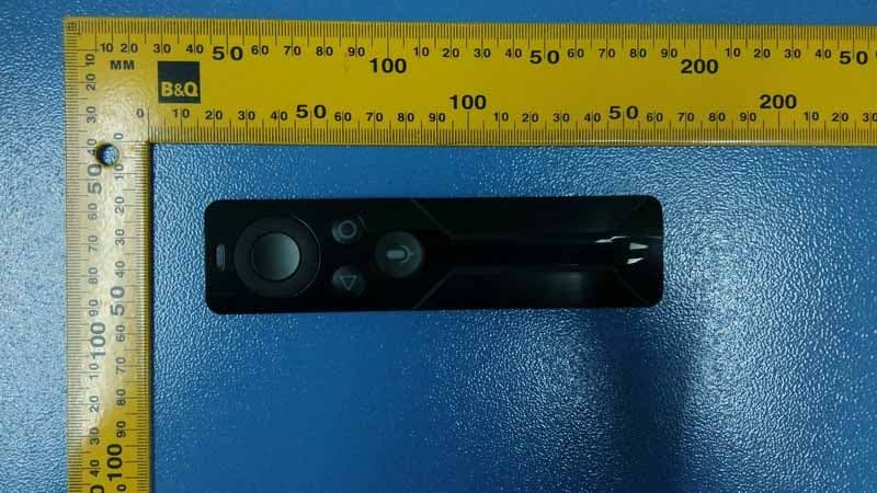
VOB-P2575
Apr 08, 2015Remote Control
Equipment Class
DSS - Part 15 Spread Spectrum Transmitter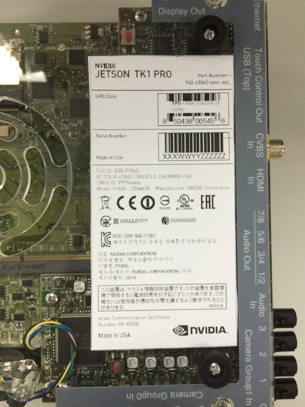
VOB-P1860
Apr 01, 2015Development Platform
Equipment Class
NII - Unlicensed National Information Infrastructure TX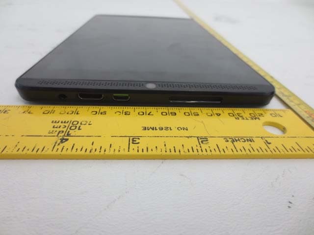
VOB-P1761WX
Mar 15, 2015Tablet
Equipment Class
DTS - Digital Transmission System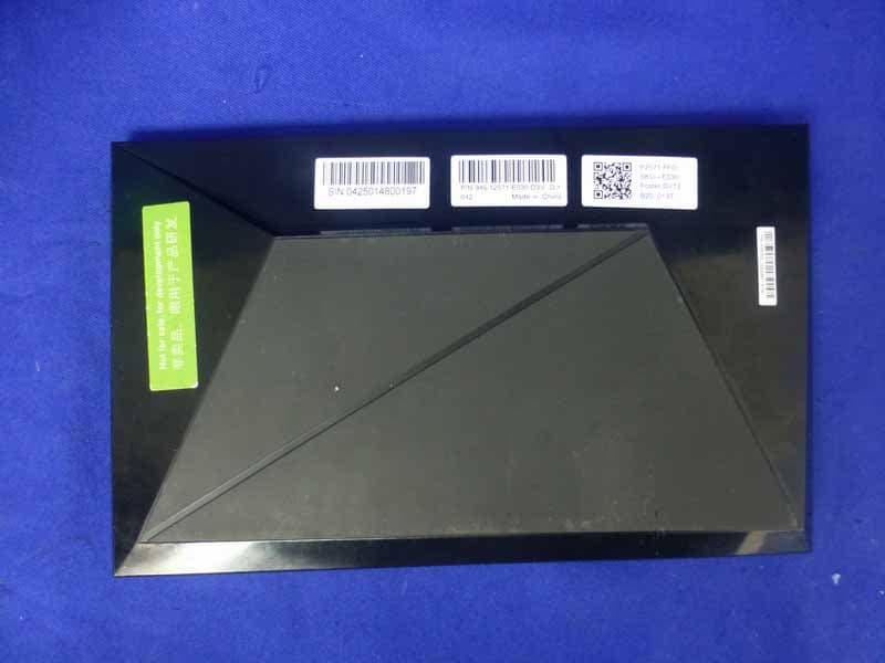
VOB-P2571
Mar 11, 2015Complex Set-Top Box
Equipment Class
DTS - Digital Transmission System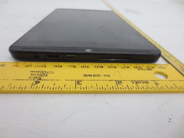
VOB-P1761W
Jun 15, 2014Tegra K1 Tablet
Equipment Class
DSS - Part 15 Spread Spectrum Transmitter