XPYJODYW263WLAN/Bluetooth host-based multiradio module JODY-W2
u-blox AG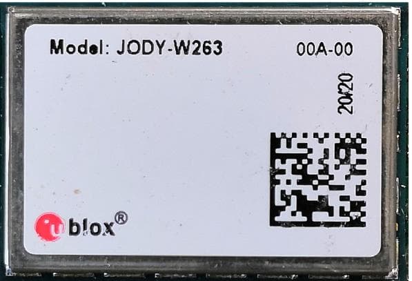
Click to zoom
Application Details
- Equipment Class
- NII - Unlicensed National Information Infrastructure TX
- Date of Grant
- Apr 27, 2021
- Application Purpose
- Original Equipment
- Date of Application
- Apr 27, 2021
- Equipment Note
- WLAN/Bluetooth host-based multiradio module JODY-W2
- Frequency Range
- 5745.00000000 - 5825.00000000
- Company
- u-blox AG
- Country
- Switzerland
Documents & Files
Document Text
Text extracted from the exhibit documents filed with the FCC. Open a document above to read the original.
Users Manual
JODY-W2 Antenna reference design Application Note Abstract This application note describes the test set-up used in JODY-W2 module certification. www.u-blox.com UBX-20053581 - TBD JODY-W2 - Application Note UBX-20053581 - TBD Page 2 of 11 Document Information Title JODY-W2 Subtitle Antenna reference design Document type Application Note Document number UBX-20053581 Revision and date TBD TBD Disclosure Restriction This document applies to the following products: Product name JODY-W2 series u-blox or third parties may hold intellectual property rights in the products, names, logos and designs included in this document. Copying, reproduction, modification or disclosure to third parties of this document or any part thereof is only permitted with the express written permission of u-blox. The information contained herein is provided “as is” and u-blox assumes no liability for its use. No warranty, either express or implied, is given, including but not limited to, with respect to the accuracy, correctness, reliability and fitness for a particular purpose of the information. This document may be revised by u-blox at any time without notice. For the most recent documents, visit www.u-blox.com. Copyright © u-blox AG. JODY-W2 - Application Note UBX-20053581 - TBD Page 3 of 11 Contents Document Information ................................................................................................................................ 2 Contents .......................................................................................................................................................... 3 1 Scope ......................................................................................................................................................... 4 2 General description and requirements ........................................................................................... 4 3 Reference design of RF path .............................................................................................................. 5 3.1 RF trace PCB routing .................................................................................................................................. 5 4 Parts ........................................................................................................................................................... 8 Revision history ........................................................................................................................................... 10 Contact ............................................................................................................................................................ 11 JODY-W2 - Application Note UBX-20053581 - TBD Contents Page 4 of 11 1 Scope This document defines the essential specifications necessary to implement the JODY-W2 antenna reference designs as used in certification. It is part of the equipment certification application issued to FCC and ISED. The information contained herein and its references should be sufficient to guide a skilled person to implement the design on a host carrier. It will provide the designer with PCB layout details and expected performance specifications. This document supports a connector-based design for the use of external antennas (one for each antenna pin of the module). 2 General description and requirements JODY-W2 series modules provide two RF interfaces for connecting external antennas. The antenna ports ANT0 and ANT1 have a nominal characteristic impedance of 50 Ω and must be connected to the related antenna through a 50 Ω transmission line to allow proper impedance matching along the RF path. A bad termination of the pin may result in poor performance or even damage the RF section of the module. For optimal performance in multiradio mode, the isolation between the antennas shall target the requirements as specified in Table 1 and Table 2 in order to ensure good performance. Item Requirements Remarks Impedance 50 nominal characteristic impedance The impedance of the antenna RF connection must match the 50 impedance of the antenna pins. Frequency range 2400 - 2500 MHz 5150 - 5850 MHz For 802.11b/g/n and Bluetooth. For 802.11a/n/ac. Return loss S11 < -10 dB (VSWR < 2:1) recommended S11 < -6 dB (VSWR < 3:1) acceptable The return loss or the S11, as the VSWR, refers to the amount of reflected power, measuring how well the primary antenna RF connection matches the 50 characteristic impedance of antenna pins. The impedance of the antenna termination must match as much as possible the 50 nominal impedance of antenna pins over the operating frequency range, to maximize the amount of power transferred to the antenna. Efficiency > -1.5 dB ( > 70% ) recommended > -3.0 dB ( > 50% ) acceptable The radiation efficiency is the ratio of the radiated power to the power delivered to antenna input: the efficiency is a measure of how well an antenna receives or transmits. Maximum gain The maximum antenna gain must not exceed the value specified in type approval documentation to comply with regulatory agencies radiation exposure limits. Table 1: Summary of antenna interface requirements Item Requirements Remarks Isolation (in-band) S 21 > 25 dB recommended S 21 > 20 dB acceptable The antenna to antenna isolation is the S 21 parameter between the two antennas in the band of operation. Isolation (out-of-band) S 21 > 35 dB recommended S 21 > 30 dB acceptable Out-of-band isolation is evaluated in the band of the aggressor to ensure that the transmitting signal from the other radio is sufficiently attenuated by the receiving antenna to avoid saturation and intermodulation effect at the receiver’s port. Envelope correlation Coefficient (ECC) ECC < 0.1 recommended ECC < 0.5 acceptable The ECC parameter correlates the far field parameters between antennas in the same system. A low ECC parameter is fundamental to improve performance in MIMO-based systems. Table 2: Summary of MIMO…
Text truncated - open the document above for the full version.
Users Manual
UBX-18017567 - R07 C1 - Public www.u-blox.com JODY-W2 series Host-based multiradio modules with Wi-Fi and Bluetooth 5 Data sheet Abstract This technical data sheet describes the JODY-W2 series modules with 1x1 802.11n/ac and dual-mode Bluetooth 5. JODY-W2 is ideal for in-vehicle infotainment and telematics applications with simultaneous use cases requiring high data rates, such as in-car hotspots, Wi-Fi display applications such as Apple CarPlay, or video streaming across multiple clients. Connection to a host processor is through SDIO, or High-Speed UART interfaces (Bluetooth only). JODY-W2 series - Data sheet UBX-18017567 - R07 Document information Page 2 of 46 C1 - Public Document information Title JODY-W2 series Subtitle Host-based multiradio modules with Wi-Fi and Bluetooth 5 Document type Data sheet Document number UBX-18017567 Revision and date R07 28-Jan-2021 Disclosure restriction C1 - Public Product status Corresponding content status Functional Sample Draft For functional testing. Revised and supplementary data will be published later. In Development / Prototype Objective specification Target values. Revised and supplementary data will be published later. Engineering Sample Advance information Data based on early testing. Revised and supplementary data will be published later. Initial Production Early production information Data from product verification. Revised and supplementary data may be published later. Mass Production / End of Life Production information Document contains the final product specification. This document applies to the following products: Product name Type number Chipset PCN reference Product status JODY-W263-A JODY-W263-00A-00 88W8987A N/A Initial production JODY-W263-A JODY-W263-01A-00 88W8987S N/A Initial production JODY-W263 JODY-W263-00B-00 88W8987 N/A Initial production u-blox or third parties may hold intellectual property rights in the products, names, logos and designs included in this document. Copying, reproduction, modification or disclosure to third parties of this document or any part thereof is only permitted with the express written permission of u-blox. The information contained herein is provided “as is” and u-blox assumes no liability for its use. No warranty, either express or implied, is given, including but not limited to, with respect to the accuracy, correctness, reliability and fitness for a particular purpose of the information. This document may be revised by u-blox at any time without notice. For the most recent documents, visit www.u-blox.com. Copyright © u-blox AG. JODY-W2 series - Data sheet UBX-18017567 - R07 Contents Page 3 of 46 C1 - Public Contents Document information ................................................................................................................................ 2 Contents .......................................................................................................................................................... 3 1 Functional description ......................................................................................................................... 5 1.1 Overview ........................................................................................................................................................ 5 1.2 Applications ................................................................................................................................................. 5 1.3 Block diagram .............................................................................................................................................. 6 1.4 Product features ......................................................................................................................................... 7 1.4.1 Wi-Fi features ...................................................................................................................................... 7 1.4.2 Wi-Fi Simultaneous operation modes ............................................................................................ 8 1.4.3 Bluetooth features ............................................................................................................................. 8 1.4.4 General product features .................................................................................................................. 8 1.4.5 Reserved MAC addresses ................................................................................................................. 8 2 Interfaces ................................................................................................................................................. 9 2.1 Host interface configuration .................................................................................................................... 9 2.2 SDIO interface .............................................................................................................................................. 9 2.2.1 Default speed and high speed modes (1.8 V) .............................................................................. 10 2.2.2 SDR12, SDR25, SDR50 modes (up to 100 MHz, 1.8 V) ................................................................ 11 2.2.3 SDR104 mode (208 MHz, 1.8 V) .......................................................................................................12 2.2.4 DDR50 Mode (50 MHz, 1.8 V)...........................................................................................................12 2.3 High Speed UART interface .................................................................................................................... 14 2.4 PCM Interface ............................................................................................................................................ 15 2.4.1 PCM Interface specifications ......................................................................................................... 15 2.…
Text truncated - open the document above for the full version.
Cover Letter(s)
THIS MUST BE SIGNED BY THE APPLICANT/AGENT AND SHOULD BE PLACED ON APPROPRIATE LETTERHEAD 053019-02a Request for Modular/Limited Modular Approval Date: January 8, 2021 Subject: Manufacturer’s Declaration for ☒ - Modular Approval ☐ - Split Modular Approval ☐ - Limited Modular Approval ☐ - Limited Split Modular Approval Confidentiality Request for: XPYJODYW263 8 Basic Requirements – FCC Part 15.212(a)(1) For Items Marked “NO(*)”, the Limited Module Description Must be Filled Out on the Following Pages Modular Approval Requirement Requirement Met 1. The modular transmitter must have its own RF shielding. This is intended to ensure that the module does not have to rely upon the shielding provided by the device into which it is installed in order for all modular transmitter emissions to comply with FCC limits. It is also intended to prevent coupling between the RF circuitry of the module and any wires or circuits in the device into which the module is installed. Such coupling may result in non-compliant operation. The physical crystal and tuning capacitors may be located external to the shielded radio elements. 15.212(a)(1)(i) ☒ - YES ☐ - NO(*) 2. The modular transmitter must have buffered modulation/data inputs (if such inputs are provided) to ensure that the module will comply with FCC requirements under conditions of excessive data rates or over-modulation. 15.212(a)(1)(ii) ☒ - YES ☐ - NO(*) 3. The modular transmitter must have its own power supply regulation on the module. This is intended to ensure that the module will comply with FCC requirements regardless of the design of the power supplying circuitry in the device into which the module is installed. 15.212(a)(1)(iii) ☒ - YES ☐ - NO(*) 4. The modular transmitter must comply with the antenna and transmission system requirements of §§ 15.203, 15.204(b), 15.204(c), 15.212(a), and 2.929(b). The antenna must either be permanently attached or employ a ‘‘unique’’ antenna coupler (at all connections between the module and the antenna, including the cable). The ‘‘professional installation’’ provision of § 15.203 is not applicable to modules but can apply to limited modular approvals under paragraph 15.212(b). 15.212(a)(1)(iv) ☒ - YES ☐ - NO(*) 5. The modular transmitter must be tested in a stand-alone configuration, i.e., the module must not be inside another device during testing. This is intended to demonstrate that the module is capable of complying with Part 15 emission limits regardless of the device into which it is eventually installed. Unless the transmitter module will be battery powered, it must comply with the AC line conducted requirements found in Section 15.207. AC or DC power lines and data input/output lines connected to the module must not contain ferrites, unless they will be marketed with the module (see Section 15.27(a)). The length of these lines shall be length typical of actual use or, if that length is unknown, at least 10 centimeters to insure that there is no coupling between the case of the module and supporting equipment. Any accessories, peripherals, or support equipment connected to the module during testing shall be unmodified or commercially available (see Section 15.31(i)). 15.212(a)(1)(v) ☒ - YES ☐ - NO(*) THIS MUST BE SIGNED BY THE APPLICANT/AGENT AND SHOULD BE PLACED ON APPROPRIATE LETTERHEAD 053019-02a Modular Approval Requirement Requirement Met 6. The modular transmitter must be labeled with its own FCC ID number, or use an electron display (see KDB Publication 784748). If using a permanently affixed label with its own FCC ID number, if the FCC ID is not visible when the module is installed inside another device, then the outside of the device into which the module is installed must also display a label referring to the enclosed module. This exterior label can use wording such as the following: “Contains Transmitter Module FCC ID: XYZMODEL1” or “Contains FCC ID: XYZMODEL1.” Any similar wording that expresses the same meaning may be used. The Grantee may either provide such a label, an example of which must be included in the application for equipment authorization, or, must provide adequate instructions along with the module which explain this requirement. In the latter case, a copy of these instructions must be included in the application for equipment authorization. If the modular transmitter uses an electronic display of the FCC identification number, the information must be readily accessible and visible on the modular transmitter or on the device in which it is installed. If the module is installed inside another device, then the outside of the device into which the module is installed must display a label referring to the enclosed module. This exterior label can use wording such as the following: “Contains FCC certified transmitter module(s).” Any similar wording that expresses the same meaning may be used. The user manual must include instructions on how to access the electronic display. A copy of these instructions must be included in the application for equipment authorization. 15.212(a)(1)(vi) ☒ - YES ☐ - NO(*) 7. The modular transmitter must comply with all specific rule or operating requirements applicable to the transmitter, including all the conditions provided in the integration instructions by the grantee. A copy of these instructions must be included in the application for equipment authorization. For example, there are very strict operational and timing requirements that must be met before a transmitter is authorized for operation under Section 15.231. For instance, data transmission is prohibited, except for operation under Section 15.231(e), in which case there are separate field strength level and timing requirements. Compliance with these requirements must be assured. 15.212(a)(1)(vii) ☒ - YES ☐ - NO(*) 8. The modular transmitter must comply with any applicable RF exposure requirements. For example, FCC Rules in Sections 2.1091, 2.1093 and specific Sections of Part 15, including 15.3…
Text truncated - open the document above for the full version.
External Photos
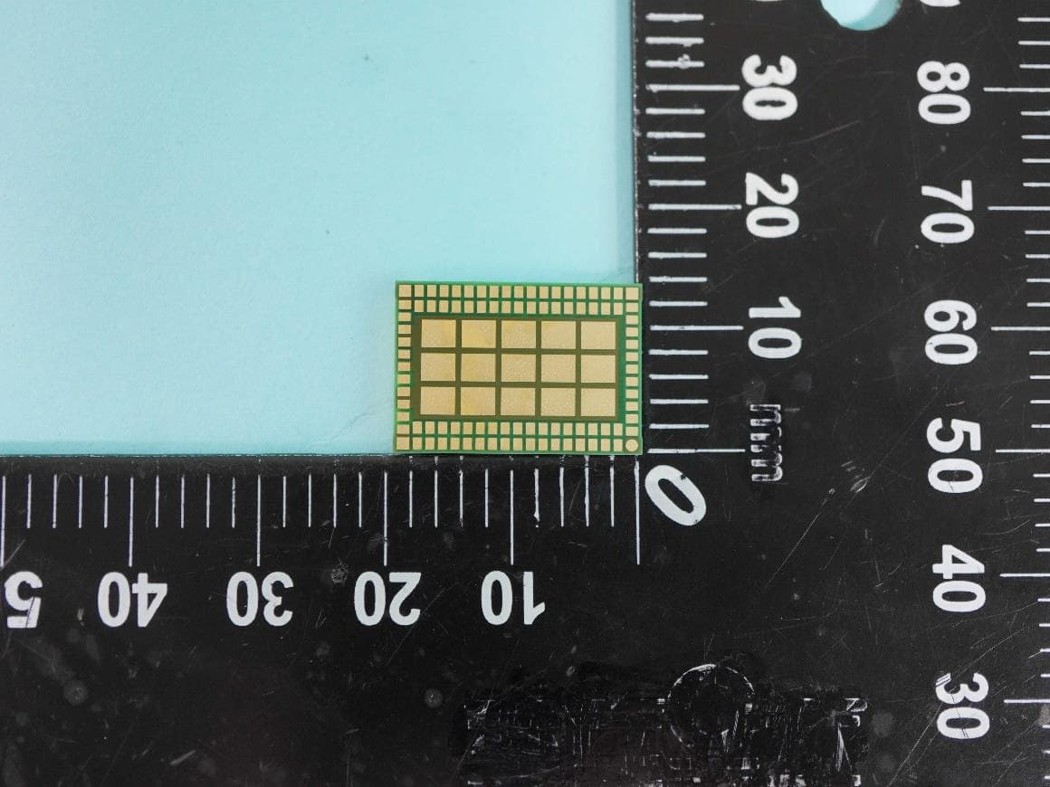
JODY-W2 photos UBX-18017912 Page 1 of 3 JODY-W2 photos Topic : JODY-W2 photos Doc.No: UBX-18017912 Revision R01 Date: Name Signature Created 15-Dec-2020 Franck Campagna frca Checked Released 15-Dec-2020 Franck Campagna frca We reserve all rights in this document and in the information contained therein. Reproduction, use or disclosure to third parties without express authority is strictly forbidden. © 20168 u-blox AG 1 Scope This document provides internal and external photos of the JODY-W263-01A and JODY-W164-07A modules. It is part of the equipment certification application issued to FCC and ISED. The photos have been taken with the RF shield mounted and removed. 2 FCC/IC ID reference Ordering Code(s) FCC ID ISED ID JODY-W263-01A JODY-W263-00A JODY-W263-00B XPYJODYW263 8595A-JODYW263 Table 1: FCC and IC IDs for different models of JODY-W2 series JODY-W2 photos UBX-18017912 Page 2 of 3 3 Top view 3.1 Internal photos Figure 1: JODY-W263-01A, JODY-W263-00A and JODY-W263-00B internal photo JODY-W2 photos UBX-18017912 Page 3 of 3 3.2 External photos Figure 2: JODY-W263-00A top view external photo Figure 3: JODY-W263-00A top view external photo Figure 4: JODY-W263-00B top view external photo 4 Bottom view Figure 2: Bottom view for all module variants
ID Label/Location Info
UBX-20058689 1/3 JODY-W2 Label and location Author Date To Topic JODY-W2 Label and location JODY-W2 Label and location UBX-20058689 Franck Campagna 15 December 2020 Certification application reviewer Copying, reproduction, modification or disclosure to third parties of this document or any part thereof is only permitted with the express written permission of u-blox. The information contained herein is provided “as is” and u-blox assumes no liability for its use. No warranty, either express or implied, is given, including but not limited, with respect to the accuracy, correctness, reliability and fitness for a particular purpose of the information. This document may be revised by u-blox at any time. For most recent documents, visit www.u-blox.com. Copyright© u-blox AG. 1 Scope This document provides information on JODY-W2 series modules’ label contents and location on the module. It is part of the equipment certification application issued to FCC and ISED. 2 FCC/ISED ID reference JODY-W263-01A JODY-W263-00A JODY-W263-00B XPYJODYW263 8595A-JODYW263 Table 1: FCC and ISED IDs for different models of JODY-W2 series modules 3 Label 3.1 Label specification The labels of JODY-W2 series include important product information as described in this section. The data matrix code for automotive and professional grade variants of JODY-W2 series includes a serial number. Figure 1 illustrates the sample label of the JODY-W2 series and includes: the u-blox logo, product name (model), type number, FCC and ISED certification number and date of unit production encoded YY/WW (year/week). UBX-20058689 2/3 JODY-W2 Label and location Figure 1: JODY-W2 series sample label A detailed description of the label components are listed in Table 2. Table 2: JODY-W2 series label description The model name, which is identical to the ordering code, used for product type approval is shown on the first line of the label. Table 3 provides the mapping of ordering code, label contents and FCC/ISED IDs. The marking “xx” in Reference 2 on the label is the minor product version and not relevant for certification. JODY-W263-01A JODY-W263-00A JODY-W263-00B JODY-W263-01A JODY-W263-00A JODY-W263-00B xx xx xx XPYJODYW263 8595A-JODYW263 Table 3: Mapping of ordering code, label marking and FCC/ISED IDs. 3.2 Product labels FCC ID: XPYJODYW263 IC: 8595A-JODYW263 1 2 3 4 5 6 UBX-20058689 3/3 JODY-W2 Label and location Figure 2: JODY-W263-01A label Figure 3: JODY-W263-00A label Figure 4: JODY-W263-00B label 4 Label location The label is placed on top of the shield of the JODY-W2 series modules as shown below Figure 5: JODY-W2 series label location
Internal Photos
JODY-W2 photos UBX-18017912 Page 1 of 3 JODY-W2 photos Topic : JODY-W2 photos Doc.No: UBX-18017912 Revision R01 Date: Name Signature Created 15-Dec-2020 Franck Campagna frca Checked Released 15-Dec-2020 Franck Campagna frca We reserve all rights in this document and in the information contained therein. Reproduction, use or disclosure to third parties without express authority is strictly forbidden. © 20168 u-blox AG 1 Scope This document provides internal and external photos of the JODY-W263-01A and JODY-W164-07A modules. It is part of the equipment certification application issued to FCC and ISED. The photos have been taken with the RF shield mounted and removed. 2 FCC/IC ID reference Ordering Code(s) FCC ID ISED ID JODY-W263-01A JODY-W263-00A JODY-W263-00B XPYJODYW263 8595A-JODYW263 Table 1: FCC and IC IDs for different models of JODY-W2 series JODY-W2 photos UBX-18017912 Page 2 of 3 3 Top view 3.1 Internal photos Figure 1: JODY-W263-01A, JODY-W263-00A and JODY-W263-00B internal photo JODY-W2 photos UBX-18017912 Page 3 of 3 3.2 External photos Figure 2: JODY-W263-00A top view external photo Figure 3: JODY-W263-00A top view external photo Figure 4: JODY-W263-00B top view external photo 4 Bottom view Figure 2: Bottom view for all module variants
RF Exposure Info
RF Exposure evaluation for mobile devices Model: JODY-W263-01A, JODY-W263-00A, JODY-W263-00B FCC ID: XPYJODYW263 IC: 8595A- JODYW263 Standards OET Bulletin 65 Edition 97-01 August 1997 FCC 47 CFR §1.1307 FCC 47 CFR §1.1310 RSS-102 Issue 5 – March 2015 Test limits As specified in Table 1B of 47 CFR 1.1310 – Limits for Maximum Permissible Exposure (MPE), Limits for General Population/Uncontrolled Exposure. Frequency range (MHz) Power density (mW/cm²) 300 – 1,500 f/1500 1,500 – 100,000 1.0 Limits specified per RSS-102, Issue 5. Frequency range (MHz) Power density (W/m²) Power density (mW/cm²) 300 – 6000 0.02619 f 0.6834 mW/cm² = W/m² * 0.1 Equation OET bulletin 65, page 18, edition 97-01: Where: S = power density P = power input to the antenna G = power gain of the antenna in the direction of interest relative to an isotropic radiator R = distance to the center of radiation of the antenna = 20cm Operational Bands Frequency (MHz) Antenna Gain (dBi) Antenna Gain -numeric- (mW/cm²) Output Power -conducted- (dBm) Duty Cycle correctio n factor Max. mean output power (dBm) Output Power -conducted- (mW) Output Power (EIRP) (mW) IC Limit (mW/cm²) FCC Limit (mW/cm²) Power Density value (mW/cm²) Margin to FCC Limit (mW/cm²) Margin to IC Limit (mW/cm²) BLE24802.21.65964.0004.002.514.170.54691.000.00080.99920.5461 Classic BT24802.21.659611.00011.0012.5920.890.54691.000.00420.99580.5427 WLAN 2.4 GHz24572.51.778316.00016.0039.8170.790.54341.000.01410.98590.5293 WLAN 5 GHz57454.62.884016.00016.0039.81114.820.97101.000.02280.97720.9482 Simultaneous Transmission Considerations The calculation below is used to consider situations in which simultaneous exposure to fields of different frequencies occur. The calculation is performed by the sum of each relative exposure for each equipment according to the following criteria. Where: S eq is the power density of the electromagnetic field at a given distance by a specific transmitter and a defined frequency. S lim is the MPE limit for the frequency being evaluated. Assessment of Simultaneous transmission for FCC Classic BT WLAN 5 GHz WLAN 2.4 GHz (S eq / S Lim ) 0.0042 0.0228 0.0141 Sum of (S eqn / S Limn ) BT + WLAN 2.4 GHz 0.0183 Sum of (S eqn / S Limn ) BT + WLAN 5 GHz 0.027 Limit 1 Assessment passed Assessment of Simultaneous transmission for ISED Classic BT WLAN 5 GHz WLAN 2.4 GHz (S eq / S Lim ) 0.0077 0.0235 0.0259 Sum of (S eqn / S Limn ) BT + WLAN 2.4 GHz 0.0336 Sum of (S eqn / S Limn ) BT + WLAN 5 GHz 0.0312 Limit 1 Assessment passed Co-Location Considerations with Cellular modem SARA-R510M8S as example FCC BandMode Duty Cycle (%) Frequency (MHZ) Maximum Conducted output power (dBm) Max Conducted output power (mW) FCC MPE Limit (mW/cm²) Power Density (mW/cm²) Separation distance (cm)Verdict 850 GSM 50%848.833.251056.820.56590.528120Pass 1900 GSM 50%1909.830.2523.601.00000.186520Pass FDD 2 UMTS 100%1907.624.5281.841.00000.505520Pass FDD 4 UMTS 100%1740.024.5281.841.00000.230520Pass FDD 5 UMTS 100%836.024.5281.840.55730.523320Pass eFDD 2 LTE 100%1908.024251.191.00000.363720Pass eFDD 4 LTE 100%1755.024251.191.00000.233220Pass eFDD 5 LTE 100%826.524251.190.55100.511420Pass eFDD 7 LTE 100%2535.024251.191.00000.222720Pass eFDD 13 LTE 100%782.224251.190.52150.485120Pass eFDD 17 LTE 100%716.024251.190.47730.442420Pass eFDD 12 LTE 100%711.024251.190.47400.237520Pass eFDD 30 LTE 100%2310.024251.191.00000.011020Pass eFDD 66 LTE 100%1770.024251.191.00000.377320Pass eTDD 41 LTE 100%2680.024251.191.00000.408120Pass eFDD 25 LTE 100%1855.024251.191.23670.363720Pass eFDD 26 LTE 100%814.024251.190.54270.222220Pass ISED BandMode Duty Cycle (%) Frequency (MHZ) Maximum Conducted output power (dBm) Max Conducted output power (mW) FCC MPE Limit (mW/cm²) Power Density (mW/cm²) Separation distance (cm)Verdict 850 GSM 50%848.833.251056.820.26280.235920Pass 1900 GSM 50%1909.830.2523.600.45750.186520Pass FDD 2 UMTS 100%1907.624.5281.840.45710.407220Pass FDD 4 UMTS 100%1740.024.5281.840.42930.230520Pass FDD 5 UMTS 100%836.024.5281.840.26010.233720Pass eFDD 2 LTE 100%1908.024251.190.45720.363720Pass eFDD 4 LTE 100%1755.024251.190.43180.233220Pass eFDD 5 LTE 100%826.524251.190.25810.228420Pass eFDD 7 LTE 100%2535.024251.190.55520.222720Pass eFDD 13 LTE 100%782.224251.190.24860.223220Pass eFDD 17 LTE 100%716.024251.190.23400.208320Pass eFDD 12 LTE 100%711.024251.190.23290.208320Pass eFDD 30 LTE 100%2310.024251.190.52100.011020Pass eFDD 66 LTE 100%1770.024251.190.43430.377320Pass eTDD 41 LTE 100%2680.024251.190.57670.408120Pass eFDD 25 LTE 100%1855.024251.190.44850.363720Pass eFDD 26 LTE 100%814.024251.190.25540.222220Pass Relative exposure for Secondary Transmitter for FCC OP-ModeMode Output Power (mW) Frequency (MHZ) S eq (mW/cm²) S lin (mW/cm²) S eq ----------- S Lin Verdict 850GSM1056.8175848.80.52810.56590.9332895Pass 1900GSM523.60041909.80.18651.00000.1865351Pass FDD 2UMTS281.83831907.60.50551.00000.5055458Pass FDD 4UMTS281.83831740.00.23051.00000.2305316Pass FDD 5UMTS281.8383836.00.52330.55730.9388917Pass eFDD 2LTE251.18861908.00.36371.00000.3637144Pass eFDD 4LTE251.18861755.00.23321.00000.2332011Pass eFDD 5LTE251.1886826.50.51140.55100.9280661Pass eFDD 7LTE251.18862535.00.22271.00000.2227053Pass eFDD 13LTE251.1886782.20.48510.52150.9303166Pass eFDD 17LTE251.1886716.00.44240.47730.9268939Pass eFDD 12LTE251.1886711.00.23750.47400.501132Pass eFDD 30LTE251.18862310.00.01101.00000.0109825Pass eFDD 66LTE251.18861770.00.37731.00000.377338Pass eTDD 41LTE251.18862680.00.40811.00000.4080943Pass eFDD 25LTE251.18861855.00.36371.23670.2941087Pass eFDD 26LTE251.1886814.00.22220.54270.4094467Pass Relative exposure for Primary Transmitter for ISED OP-Mode Mode Output Power (mW) Frequency (MHZ) S eq (mW/cm²) S lin (mW/cm²) S eq ----------- S Lin Verdict 850 GSM 1056.8175 848.8 0.2359 0.2628 0.8975309 Pass 1900 GSM 523.6004 1909.8 0.1865 0.4575 0.4077537 Pass FDD 2 UMTS 281.8383 1907.6 0.4072 0.4571 0.8907175 Pass FDD 4 UMTS 281.8383 1740.0 0.2305 0.4293 0.5370363 Pass FDD 5 UMTS 281.8383 836.0 0.…
Text truncated - open the document above for the full version.
Test Report
Test Laboratory: 7layers GmbH Borsigstrasse 11 40880 Ratingen Germany Note: The following test results relate only to the devices specified in this document. This report shall not be reproduced in parts without the written approval of the test laboratory. 7layers GmbHGeschäftsführer/ Borsigstraße 11Managing Directors:Registergericht/registered:a Bureau Veritas 40880 Ratingen, Germany Frank SpillerDüsseldorf HRB 75554Group Company T +49 (0) 2102 749 0Bernhard RetkaUSt-Id.-Nr./VAT-No. DE203159652 F +49 (0) 2102 749 350Alexandre Norré-OudardSteuer-Nr./TAX-No. 147/5869/0385www.7layers.com Commerzbank AG Account No. 303 016 000 Bank Code 300 400 00 IBAN DE81 3004 0000 0303 0160 00 Swift Code COBADEFF FCC Measurement/Technical Report on WLAN and Bluetooth module JODY-W2 FCC ID: XPYJODYW263 IC: 8595A-JODYW…
Text truncated - open the document above for the full version.
Contact Information
Applicant
Giulio Comar(Certification Manager)
Test Firm
7layers GmbHBernhard Retka
Technical Specifications
| # | Rule Parts | Frequency Range | Power Output |
|---|---|---|---|
| 4 | 15E | 5.75 GHz - 5.83 GHz | 32.00 mW |
Other Applications from u-blox AG
XPYJODYB1
Aug 07, 2026BT Module
Equipment Class
DSS - Part 15 Spread Spectrum Transmitter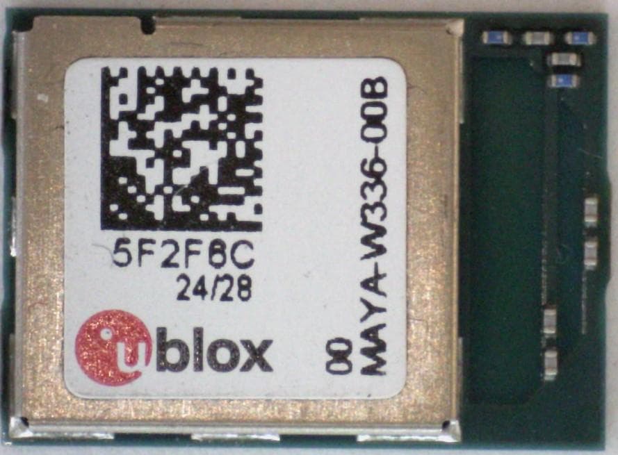
XPYMAYAW3A
Feb 01, 2026WLAN and Bluetooth module
Equipment Class
6XD - 15E 6 GHz Low Power Indoor Client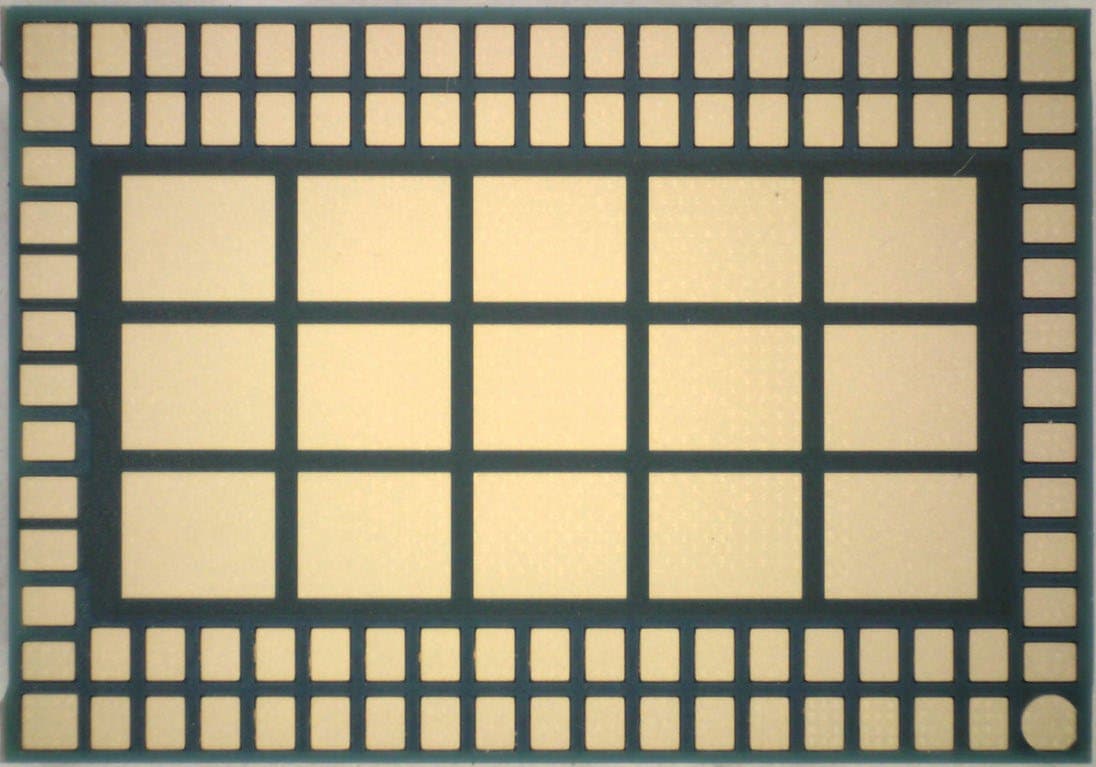
XPYJODYW6A
Jan 22, 2026WLAN and Bluetooth module
Equipment Class
NII - Unlicensed National Information Infrastructure TXXPYUBX22VA03
Jul 22, 2024NB CatM EGPRS data only module
Equipment Class
PCB - PCS Licensed Transmitter
XPYIRISW1
Jul 21, 2024Stand-alone Tri-radio wireless MCU module
Equipment Class
DTS - Digital Transmission System