XPYMAYAW160WLAN/Bluetooth host-based multiradio module MAYA W160
u-blox AG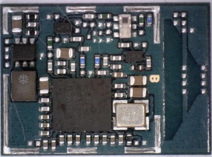
Click to zoom
Application Details
- Equipment Class
- NII - Unlicensed National Information Infrastructure TX
- Date of Grant
- Nov 23, 2022
- Application Purpose
- Original Equipment
- Date of Application
- Nov 22, 2022
- Equipment Note
- WLAN/Bluetooth host-based multiradio module MAYA W160
- Frequency Range
- 5745.00000000 - 5825.00000000
- Company
- u-blox AG
- Country
- Switzerland
Documents & Files
Document Text
Text extracted from the exhibit documents filed with the FCC. Open a document above to read the original.
Users Manual
UBX-21010495 - R04 C2-Restricted www.u-blox.com MAYA-W1 series Host-based modules with Wi-Fi and Bluetooth System integration manual Abstract This document describes the system Integration of MAYA-W1 series short range modules with dual- band Wi-Fi 4 and Bluetooth 5.1. These host-based modules are ultra-compact cost-efficient multiradio modules in the MAYA form factor, designed for a wide range of industrial applications. This module series includes variants with or without internal antenna. It includes an integrated MAC/Baseband processor and RF front end components. It can connect to a host processor through its SDIO and High-Speed UART interfaces. MAYA-W1 series - System integration manual UBX-21010495 - R04 Document information Page 2 of 64 C2-Restricted Document information Title MAYA-W1 series Subtitle Host-based modules with Wi-Fi and Bluetooth Document type System integration manual Document number UBX-21010495 Revision and date R04 4-Jul-2022 Disclosure Restriction C2-Restricted Document status explanation Draft For functional testing. Revised and supplementary data will be published later. Objective Specification Target values. Revised and supplementary data will be published later. Advance Information Data based on early testing. Revised and supplementary data will be published later. Early Production Information Data from product verification. Revised and supplementary data may be published later. Production Information Document contains the final product specification. This document applies to the following products: Product name Type number MAYA-W160 MAYA-W160-00B-00 MAYA-W161 MAYA-W161-00B-00 MAYA-W166 MAYA-W166-00B-00 MAYA-W166 MAYA-W166-01B-00 ☞ For information about the related hardware, software, and status of listed product types, see also the respective data sheets [1]. u-blox or third parties may hold intellectual property rights in the products, names, logos and designs included in this document. Copying, reproduction, modification or disclosure to third parties of this document or any part thereof is only permitted with the express written permission of u-blox. The information contained herein is provided “as is” and u-blox assumes no liability for its use. No warranty, either express or implied, is given, including but not limited to, with respect to the accuracy, correctness, reliability and fitness for a particular purpose of the information. This document may be revised by u-blox at any time without notice. For the most recent documents, visit www.u-blox.com. Copyright © u-blox AG. u-blox or third parties may hold intellectual property rights in the products, names, logos and designs included in this document. Copying, reproduction, modification or disclosure to third parties of this document or any part thereof is only permitted with the express written permission of u-blox. The information contained herein is provided “as is” and u-blox assumes no liability for its use. No warranty, either express or implied, is given, including but not limited to, with respect to the accuracy, correctness, reliability and fitness for a particular purpose of the information. This document may be revised by u-blox at any time without notice. For the most recent documents, visit www.u-blox.com. Copyright © u-blox AG. MAYA-W1 series - System integration manual UBX-21010495 - R04 Contents Page 3 of 64 C2-Restricted Contents Document information ................................................................................................................................ 2 Contents .......................................................................................................................................................... 3 1 System description ............................................................................................................................... 6 1.1 Overview ........................................................................................................................................................ 6 1.2 Module architecture ................................................................................................................................... 6 1.2.1 Block diagrams .................................................................................................................................... 7 2 Pin definition ........................................................................................................................................... 9 2.1 Pin attributes ............................................................................................................................................... 9 2.2 Pin assignment ............................................................................................................................................ 9 2.3 Pin list ..........................................................................................................................................................10 3 Module integration ............................................................................................................................. 13 3.1 Power supply interface.............................................................................................................................14 3.1.1 Digital I/O interfaces reference voltage (VIO) .............................................................................14 3.2 Antenna interfaces ...................................................................................................................................15 3.2.1 Approved antenna designs (pending) ..........................................................................................15 3.2.2 MAYA-W160, MAYA-W161, and MAYA-W166-01B ................................................................15 3.2.3 MAYA-W166-00B .............................................................................................................................16 3.3 Syste…
Text truncated - open the document above for the full version.
Block Diagram
locate, communicate, accelerate RE: Certification Application Product family: MAYA-W1 Models: MAYA-W160, MAYA-W161, MAYA-W166 Block Diagram of the MAYA-W1 series modules Figure 1: Block diagram of MAYA-166 Registered office: u-blox AG Zürcherstrasse 68 8800 Thalwil Switzerland Company number: CH-020.3.020.161-7 [email protected] [email protected] Figure 2: Block diagram of MAYA-161 or MAYA-160
Cover Letter(s)
05 3019-02a Request for Modular/Limited Modular Approval Date: September 9, 2022 Subject: Manufacturer’s Declaration for ☒ - Modular Approval ☐- Split Modular Approval ☐- Limited Modular Approval ☐ - Limited Split Modular Approval Confidentiality Request for: XPYMAYAW16 0 8 Basic Requirements – FCC Part 15.212(a)(1) For Items Marked “NO(*)”, the Limited Module Description Must be Filled Out on the Following Pages Modular Approval Requirement Requirement Met 1.The modular transmitter must have its own RF shielding. This is intended to ensure that the module does not have to rely upon the shielding provided by the device into which it is installed in order for all modular transm itter emissions to comply with FCC limits. It is also intended to prevent coupling between the RF circuitry of the module and any wires or circuits in the device into which the module is installed. Such coupling may result in non-compliant operation. The physical crystal and tuni ng c apacitors may be located external to the shielded radio elements. 15.212(a)(1)(i) ☒- YES☐- NO(*) 2.The modular transmitter must have buffered modulation/data inputs (if such inputs are provided) to ensure that the module will comply with FCC requirements under conditions of excessive da ta rates or over-modulation . 15.212 (a)(1)(ii) ☒- YES☐- NO(*) 3.The modular transmitter must have its own power supply regulation on the module. This is intended to ensure that the module will comply with FCC requirements regardless of the design of the power su pplying circuitry in the device into which the module is installed. 15.212(a)(1)(iii) ☒- YES☐- NO(*) 4.The modular transmitter must comply with the antenna and transmission system requirements of §§ 15.203, 15.204(b), 15.204(c), 15.212(a), and 2.929(b). The antenna must either be permanently attached or employ a ‘‘unique’’ antenna coupler (at all connections between the module and the a ntenna, including the cable). The ‘‘professional installation’’ provision of § 15.203 is not applicable to modules but can apply to limited modular approvals under paragraph 15.212(b). 15.212(a)(1)(iv) ☒- YES☐- NO(*) 5.The modular transmitter must be tested in a stand-alone configuration, i.e., the module must not be inside another device during testing. This is intended to demonstrate that the module is capable of complying with Part 15 emission limits regardless of the device into which it is eventually installed. Unless the transmitter module will be battery powered, it must comply with the AC line conducted requirements found in Section 15.207. AC or DC power lines and data input/output lines connected to the module must not contain ferrites, unless they will be marketed with the module (see Section 15.27(a)). The length of these lines shall be length typical of actual use or, if that length is unknown, at lea st 10 centimeters to insure that there is no coupling between the case of the module and supporting e quipment. Any accessories, peripherals, or support equipment connected to the module during test ing shall b e unmodified or commerciall y available (see Section 15.31(i)). 15.212(a)(1)(v) ☒- YES☐- NO(*) 053019-02a Modular Approval Requirement Requirement Met 6. The modular transmitter must be labeled with its own FCC ID number, or use an electron display (see KDB Publication 784748). If using a permanently affixed label with its own FCC ID number, if the FCC ID is not visible when the module is installed inside another device, then the outside of the device into which the module is installed must also display a label referring to the enclosed module. This exterior label can use wording such as the following: “Contains Transmitter Module FCC ID: XYZMODEL1” or “Contains FCC ID: XYZMODEL1.” Any similar wording that expresses the same meaning may be used. The Grantee may either provide such a label, an example of which must be included in the application for equipment authorization, or, must provide adequate instructions along with the module which explain this requirement. In the latter case, a copy of these instructions must be included in the application for equipment authorization. If the modular transmitter uses an electronic display of the FCC identification number, the information must be readily accessible and visible on the modular transmitter or on the device in which it is installed. If the module is installed inside another device, then the outside of the device into which the module is installed must display a label referring to the enclosed module. This exterior label can use wording such as the following: “Contains FCC certified transmitter module(s).” Any similar wording that expresses the same meaning may be used. The user manual must include instructions on how to access the electronic display. A copy of these instructions must be included in the application for e quipment authorization. 15.212(a)(1)(vi) ☒ - YES ☐ - NO(*) 7. The modular transmitter must comply with all specific rule or operating requirements applicable to the transmitter, including all the conditions provided in the integration instructions by the grantee. A copy of these instructions must be included in the application for equipment authorization. For example, there are very strict operational and timing requirements that must be met before a transmitter is authorized for operation under Section 15.231. For instance, data transmission is prohibited, except for operation under Section 15.231(e), in which case there are separate field strength level and timing requirements. Compliance with these requirements must be assured. 15.212(a)(1)(vii) ☒ - YES ☐ - NO(*) 8. The modular transmitter must comply with any applicable RF exposure requirements. For example, FCC Rules in Sections 2.1091, 2.1093 and specific Sections of Part 15, including 15.319(i), 15.407(f), 15.253(f) and 15.255(g), require that Unlicensed PCS, UNII and millimeter wave devices perform routine environmental evaluation for RF Exposure to demonstrate complia…
Text truncated - open the document above for the full version.
Cover Letter(s)
To whom it may concern, This cover letter is to address the reuse of test results for FCC and ISED certification of the MAYA‐W1 Bluetooth and WLAN Modules. Related FCC KDB: 791877 The below variants are considered: Product Description: The MAYA‐W1 line is a compact WiFI/Bluetooth module. The MAYA‐W1 is a surface mount form‐factor with connections to a host processor through SDIO and High‐Speed UART interfaces. All modules are equipped with a RF shield. Product line differences All three products, W166, W161 and W160 share the identical block diagram and parts for the 5GHz Wi ‐Fi. They only differ in the connection types. The W161 will be the primary test sample for 5GHz WLAN which is re‐used by the W160 and W166. The W161 2.4GHz radio test results will be reused by the W160. As the W160 and W161 share a common 2.4ghz Block Diagram and BOM for Wi‐Fi and BT. They only differ in the connection type. See table above for connection type. The W166 variant has differences in the BOM for 2.4GHz radios and is tested fully for Bluetooth and 2.4ghz WLAN. See block diagrams below. MAYA‐W166 Block Diagram MAYA‐W160 and MAYA‐W161 Block Diagram Testing concept: Given that the MAYA‐W166, W161 and W160 share the same 5GHz design and the MAYA‐W161 and MAYA‐W160 share the same Bluetooth and 2.4GHz WiFi design, we have determined that the below testing strategy shall sufficiently demonstrate FCC compliance. Test Case Model MAYA W161 Testing MAYA ‐ W160 MAYA ‐ W166 5GHz WiFI Spot Check operational Mode Spot Check acceptance critera Spot Check operational Mode Spot Check acceptance critera Conducted emissions on AC Mains § 15.207 Full Testing Full leverage from W161 ‐ Full leverage from W161 ‐ Occupied bandwidth § 15.403 (i) (26 dB) / § 15.407 (e) (6 dB) Full Testing Full leverage from W161 ‐ Full leverage from W161 ‐ Full Testing Full leverage from W161 ‐ Full leverage from W161 ‐ Maximum conducted output power § 15.407 (a) (1),(2),(3),(4) Full Testing Full leverage from W161 ‐ Leverage from W166 no antenna Maximum power spectral density § 15.407 (a) (1),(2),(3),(5) Full Testing Full leverage from W161 ‐ Full leverage from W161 ‐ Transmitter undesirable emissions; General Field Strength Limits, Restricted Bands 15.407 (b) § 15.209 (a) Full Testing W161 Mode with lowest delta to limit line Not greater than 25% increase in emissions and below limit line Full Testing ‐ Frequency stability § 15.407 (g) Full Testing Full leverage from W161 ‐ Full leverage from W161 ‐ Transmit Power Control (TPC) and Dynamic Frequency Selection (DFS) § 15.407 (h) Full Testing Full leverage from W161 ‐ Full leverage from W161 ‐ Antenna requirement § 15.203 / 15.204 Full Testing Full leverage from W161 ‐ Full leverage from W161 ‐ BLUETOOTH * Spot check measurements which exceed the acceptance criteria listed, shall repeat the test case in full. Conducted emissions on AC Mains § 15.207 Full Testing Full leverage from W161 ‐ Full Testing ‐ Occupied bandwidth § 15.247 (a) (2) Full Testing Full leverage from W161 ‐ Full Testing ‐ Peak conducted output power § 15.247 (b) (3), (4) Full Testing Full leverage from W161 ‐ Full Testing ‐ Transmitter spurious RF conducted emissions § 15.247 (d) Full Testing Full leverage from W161 ‐ Full Testing ‐ Transmitter spurious radiated emissions § 15.247 (d); § 15.209 (a) Full Testing W161 Mode with lowest delta to limit line Not greater than 25% increase in emissions and below limit line Full Testing Not greater than 25% increase in emissions and below limit line Band edge compliance § 15.247 (d) Full Testing Full leverage from W161 ‐ Full Testing ‐ Power density § 15.247 (e) Full Testing Full leverage from W161 ‐ Full Testing ‐ Antenna requirement § 15.203 / 15.204 Full Testing Full leverage from W161 ‐ Full Testing ‐ 2.4GHZ WiFI * Spot check measurements which exceed the acceptance criteria listed, shall repeat the test case in full. Conducted emissions on AC Mains § 15.207 Full Testing Full leverage from W161 ‐ Full Testing ‐ Occupied bandwidth § 15.247 (a) (2) Full Testing Full leverage from W161 ‐ Full Testing ‐ Peak conducted output power § 15.247 (b) (3), (4) Full Testing Full leverage from W161 ‐ Full Testing ‐ Transmitter spurious RF conducted emissions § 15.247 (d) Full Testing Full leverage from W161 ‐ Full Testing ‐ Transmitter spurious radiated emissions § 15.247 (d); § 15.209 (a) Full Testing W161 Mode with lowest delta to limit line Not greater than 25% increase in emissions and below limit line Full Testing Not greater than 25% increase in emissions and below limit line Band edge compliance § 15.247 (d) Full Testing Full leverage from W161 ‐ Full Testing ‐ Power density § 15.247 (e) Full Testing Full leverage from W161 ‐ Full Testing ‐ Antenna requirement § 15.203 / 15.204 Full Testing Full leverage from W161 ‐ Full Testing ‐ * Spot check measurements which exceed the acceptance criteria listed, shall repeat the test case in full.
Cover Letter(s)
Attn: Director of Certification Federal Communications Commission 7435 Oakland Mills Road Columbia, MD 21046 Authority to Act as Agent Model / HVIN: MAYA-W160-00B PMN: MAYA-W160-00B FCC ID: XPYMAYAW160 IC: 8595A- MAYAW160 To whom it may concern: 7Layers GmbH is authorized to act on our behalf, until otherwise notified, for applications to American Certification Body, Inc. (ACB). We certify that we are not subject to denial of federal benefits, that includes FCC benefits, pursuant to Section 5301 of the Anti-Drug Abuse Act of 1988, 21 U.S.C. 862. Further, no party, as defined in 47 CFR 1.2002 (b), to the application is subject to denial of federal benefits, that includes FCC benefits. We also declare that the information provided to the FCC is true and correct to the best of our knowledge (47 CFR 2.911(d)) and we have been informed of the grantee responsibilities (47 CFR 2.909) with regard to certified equipment. Thank you, Agency Agreement Expiration Date: 07/07/2023 Sincerely, Applicant’s Company: u-blox AG Address: Zürcher Strasse 68, CH-8800 Thalwil, Switzerland _______________________________ Filip Kruzela Job Title and Dept.: Certification Manager Registered office: u-blox AG Zürcherstrasse 68 8800 Thalwil Switzerland Company number: CH-020.3.020.161-7 [email protected] [email protected]
Cover Letter(s)
Attn: Reviewing Engineer Federal Communications Commission 7435 Oakland Mills Road Columbia, MD 21046 RE: Certification Application Model / HVIN: MAYA-W160-00B PMN: MAYA-W160-00B FCC ID: XPYMAYAW160 IC: 8595A-MAYAW160 Request for Long/Short-term Confidentiality To whom it may concern: Pursuant to sections 0.457(d) and 0.459 of CFR 47 and to avoid premature release of sensitive information prior to marketing or release of the product to the public, we hereby requests long-term confidential treatment of information accompanying this application as outlined below: Schematics Software security and software configuration description incl. software configuration control declaration Block Diagram Detailed Operational Description In addition we hereby request the following exhibits contained in this application to be temporarily (short-term confidentiality) withheld from the public disclosure for an initial period of days until: not applicable External Photos Test Setup Photos Internal Photos User’s Manual The above materials contain trade secrets and proprietary information not customarily released to the public. The public disclosure of these matters might be harmful to the applicant and provide unjustified benefits to its competitors. The applicant understands that pursuant to rule 0.457(d), disclosure of this application and all accompanying documentation will not be made before the date of the GRANT for this application. Thank you for your attention in this matter. Please contact the one signed below or the authorized agent for this filing. Thank you. Applicant’s Company: u-blox AG Address: Zürcher Strasse 68, CH-8800 Thalwil, Switzerland _______________________________ Filip Kruzela Job Title and Dept.: Certification Manager Registered office: u-blox AG Zürcherstrasse 68 8800 Thalwil Switzerland Company number: CH-020.3.020.161-7 [email protected] [email protected]
External Photos
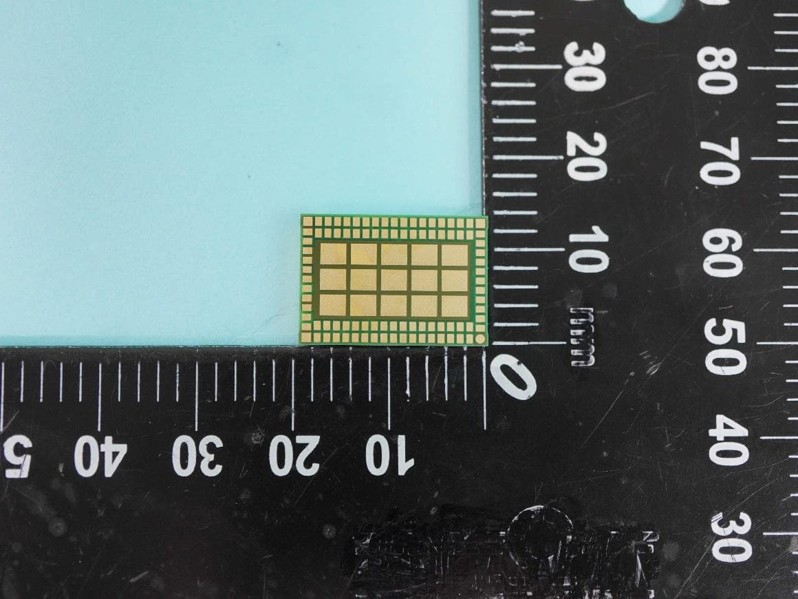
MAYA-W1 photos UBXDOC-885269510-25003 Page 1 of 4 MAYA-W1 photos Topic : MAYA-W1 photos Doc.No: UBXDOC-885269510-25003 Revision R01 Date: Name Signature Created 12-Oct-2022 Franck Campagna frca Checked Released 12-Oct-2022 Franck Campagna frca We reserve all rights in this document and in the information contained therein. Reproduction, use or disclosure to third parties without express authority is strictly forbidden. © 20168 u-blox AG 1 Scope This document provides internal and external photos of the MAYA-W1 family modules. It is part of the equipment certification application issued to FCC and ISED. The photos have been taken with the RF shield mounted and removed. 2 FCC/IC ID reference Ordering Code(s) FCC ID ISED ID MAYA-W160-00B MAYA-W161-00B MAYA-W166-00B MAYA-W166-01B XPYMAYAW160 XPYMAYAW161 XPYMAYAW166 XPYMAYAW166 8595A-MAYAW160 8595A-MAYAW161 8595A-MAYAW166 8595A-MAYAW166 Table 1: FCC and IC IDs for different models of MAYA-W1 series MAYA-W1 photos UBXDOC-885269510-25003 Page 2 of 4 3 Top view 3.1 Internal photos Figure 1: MAYA-W160-00B internal photo Figure 2: MAYA-W161-00B internal photo Figure 3: MAYA-W166-00B internal photo Figure 4: MAYA-W166-01B internal photo MAYA-W1 photos UBXDOC-885269510-25003 Page 3 of 4 3.2 External photos Figure 5: MAYA-W160-00B top view external photo Figure 6: MAYA-W161-00B top view external photo Figure 7: MAYA-W166-00B top view external photo Figure 8: MAYA-W166-01B top view external photo MAYA-W1 photos UBXDOC-885269510-25003 Page 4 of 4 4 Bottom view Figure 9: Bottom view of MAYA-W160-00B, MAYA-W161-00B, MAYA-W166-00B and MAYA-W166-01B
ID Label/Location Info
RE: Certification Application HVIN : MAYA-W160-00B, FCC ID : XPYMAYAW160, IC : 8595A-MAYAW160 HVIN : MAYA-W161-00B, FCC ID : XPYMAYAW161, IC : 8595A-MAYAW161 HVIN : MAYA-W166-00B, FCC ID : XPYMAYAW166, IC : 8595A-MAYAW166 HVIN : MAYA-W166-01B, FCC ID : XPYMAYAW166, IC : 8595A-MAYAW166 Label location information for MAYA-W1 series modules The product label is affixed on to the module shield cover as shown in Figure 1. The size of the label is 8 x 8 mm and contains the following information: • A Data Matrix formatted bar code, with a unique serial number • Date of unit production formatted YY/WW (year/week) • Major and minor product version info • Product marketing name (e.g. MAYA-W160-00B, MAYA-W161-00B, MAYA-W166-00B, MAYA-W166-01B) Figure 1: Label of the MAYA-W1 modules Figure 2: Actual size of the MAYA-W1 modules identifier marking (8 x 8 mm) Registered office: u-blox AG Zürcherstrasse 68 8800 Thalwil Switzerland Company number: CH-020.3.020.161-7 [email protected] [email protected] Figure 3: Label location of the MAYA-W1 modules The modules are SMT components shipped to the OEM-integrator on Tape&Reel packed in a sealed Dry-Pac bag and mounted onto the host board by automatic “Pick&Place” machines. As the module is a surface mount device that is soldered onto the host it is not possible to place the label on the secondary side of the module. To be able to fit the FCC/IC certification number on the label the font size has to be smaller than 4 points. Using such small font size makes the certification number too small to be readable. Therefore in accordance with CFR 47 §2.925 (f) the FCC IDs is not printed on the label but instead placed in the user manual and placed on the device packaging (e.g. Dry-Pac bag). The user manual also contains instruction on how to attach an auxiliary label on the end-product in compliance with the modular approval guidelines. The instructions will call attention to place the auxiliary label on an exterior surface of the device such that it will be visible upon inspection. The auxiliary label will have at least the information shown in 3. Figure 3: Auxiliary labels of MAYA-W1 series modules This device contains FCC ID: XPYMAYAW160 IC: 8595A-MAYAW160 This device contains FCC ID: XPYMAYAW161 IC: 8595A-MAYAW161 This device contains FCC ID: XPYMAYAW166 IC: 8595A-MAYAW166
Internal Photos
MAYA-W1 photos UBXDOC-885269510-25003 Page 1 of 4 MAYA-W1 photos Topic : MAYA-W1 photos Doc.No: UBXDOC-885269510-25003 Revision R01 Date: Name Signature Created 12-Oct-2022 Franck Campagna frca Checked Released 12-Oct-2022 Franck Campagna frca We reserve all rights in this document and in the information contained therein. Reproduction, use or disclosure to third parties without express authority is strictly forbidden. © 20168 u-blox AG 1 Scope This document provides internal and external photos of the MAYA-W1 family modules. It is part of the equipment certification application issued to FCC and ISED. The photos have been taken with the RF shield mounted and removed. 2 FCC/IC ID reference Ordering Code(s) FCC ID ISED ID MAYA-W160-00B MAYA-W161-00B MAYA-W166-00B MAYA-W166-01B XPYMAYAW160 XPYMAYAW161 XPYMAYAW166 XPYMAYAW166 8595A-MAYAW160 8595A-MAYAW161 8595A-MAYAW166 8595A-MAYAW166 Table 1: FCC and IC IDs for different models of MAYA-W1 series MAYA-W1 photos UBXDOC-885269510-25003 Page 2 of 4 3 Top view 3.1 Internal photos Figure 1: MAYA-W160-00B internal photo Figure 2: MAYA-W161-00B internal photo Figure 3: MAYA-W166-00B internal photo Figure 4: MAYA-W166-01B internal photo MAYA-W1 photos UBXDOC-885269510-25003 Page 3 of 4 3.2 External photos Figure 5: MAYA-W160-00B top view external photo Figure 6: MAYA-W161-00B top view external photo Figure 7: MAYA-W166-00B top view external photo Figure 8: MAYA-W166-01B top view external photo MAYA-W1 photos UBXDOC-885269510-25003 Page 4 of 4 4 Bottom view Figure 9: Bottom view of MAYA-W160-00B, MAYA-W161-00B, MAYA-W166-00B and MAYA-W166-01B
RF Exposure Info
RF Exposure evaluation for mobile devices Model: MAYA W160-00B FCC ID: XPYMAYAW160 IC: 8595A- MAYAW160 Standards OET Bulletin 65 Edition 97‐01 August 1997 FCC 47 CFR §1.1307 FCC 47 CFR §1.1310 RSS‐102 Issue 5 – March 2015 Test limits As specified in Table 1B of 47 CFR 1.1310 – Limits for Maximum Permissible Exposure (MPE), Limits for General Population/Uncontrolled Exposure. Frequency range (MHz) Power density (mW/cm²) 300 – 1,500 f/1500 1,500 – 100,000 1.0 Limits specified per RS S‐102, Issue 5. Frequency range (MHz) Power density (W/m²) Power density (mW/cm²) 300 – 6000 0.02619 f 0.6834 mW/cm² = W/m² * 0.1 Equ ation OET bulletin 65, page 18, edition 97‐01: Where : S = power density P = power input to the antenna G = power gain of the antenna in the direction of interest relative to an isotropic radiator R = distance to the center of radiation of the antenna = 20cm Co‐Location Considerations The calculation below is used to consider si tuations in which simultaneous exposure to fields of different frequencies occur. The calculation is performed by the sum of each relative exposure for each equipment according to the following criteria. Where: S eq is the power density of the electromagnetic field at a given distance by a specific transmitter and a defined frequency. S lim is the MPE limit for the frequency being evaluated. P S Operational Bands Ant Frequency (MHz) Antenna Gain (dBi) Output Power ‐conducted‐ (dBm) Output Power ‐conducted‐ (mW) IC Limit (mW/cm²) FCC Limit (mW/cm²) Power Density value (mW/cm²) Verdict FCC (Seq / SLim) ISED (Seq / SLim) BLE 1 2402 2.5 9.00 7.94 0.5351 1.00 0.0028 Pass 0.0028 0.0053 BLE 2 2402 2.2 9.00 7.94 0.5351 1.00 0.0026 Pass 0.0026 0.0049 BLE 3 2402 ‐3.42 9.00 7.94 0.5351 1.00 0.0007 Pass 0.0007 0.0013 Classic BT 1 2402 2.5 11.00 12.59 0.5351 1.00 0.0045 Pass 0.0045 0.0083 Classic BT 2 2402 2.2 11.00 12.59 0.5351 1.00 0.0042 Pass 0.0042 0.0078 Classic BT 3 2402 ‐3.42 11.00 12.59 0.5351 1.00 0.0011 Pass 0.0011 0.0021 WLAN 2.4 GHz 1 2412 2.5 19.00 79.43 0.5366 1.00 0.0281 Pass 0.0281 0.0524 WLAN 2.4 GHz 2 2412 2.2 19.00 79.43 0.5366 1.00 0.0262 Pass 0.0262 0.0489 WLAN 2.4 GHz 3 2412 ‐3.42 19.00 79.43 0.5366 1.00 0.0072 Pass 0.0072 0.0134 WLAN 5 GHz UNII 1 1 5240 4.6 18.00 63.10 0.9119 1.00 0.0362 Pass 0.0362 0.0397 WLAN 5 GHz UNII 1 3 5240 ‐1.51 18.00 63.10 0.9119 1.00 0.0089 Pass 0.0089 0.0097 WLAN 5 GHz UNII 2A 1 5300 4.6 18.00 63.10 0.9190 1.00 0.0362 Pass 0.0362 0.0394 WLAN 5 GHz UNII 2A 3 5300 ‐1.51 18.00 63.10 0.9190 1.00 0.0089 Pass 0.0089 0.0096 WLAN 5 GHz UNII 2C 1 5580 4.6 18.00 63.10 0.9519 1.00 0.0362 Pass 0.0362 0.0380 WLAN 5 GHz UNII 2C 3 5580 ‐1.51 18.00 63.10 0.9519 1.00 0.0089 Pass 0.0089 0.0093 WLAN 5 GHz UNII 3 1 5825 4.6 18.00 63.10 0.9803 1.00 0.0362 Pass 0.0362 0.0369 WLAN 5 GHz UNII 3 3 5825 ‐2.08 18.00 63.10 0.9803 1.00 0.0078 Pass 0.0078 0.0079 Antennas Considered Sum of (Seqn / SLimn) Max BT + Max 2.4 WLAN 0.0326 0.0607 Ant 1 ANT‐DB1‐RAF‐xxx Passed Distance to Antenna (R) in cm: 20 Ant 2 ANT‐2.4‐CW‐RCT‐xx Sum of (Seqn / SLimn) Max BT + Max 5 GHz WLAN 0.0407 0.0480 Ant 3 MAYA‐W1 PCB Trace Antenna Passed Yours sincerely, Patrick Lomax
Test Report
To whom it may con cern, This cover letter is to explain the difference between the two MAYA‐W161 and MAYA‐W160 variants and the justification for the reuse of test results: For FCC and ISED identifiers, refer to the table below. Product differences and testing reports The MAYA‐W160 and MAYA‐W161 are e lectrically equivalent. The difference between the products is in the RF termination. The W160 uses a u.FL connection for 2.4 GHz and 5 GHz, while the W161 uses and BT and WLAN pin. Both requiring 50 Ohms. (Refer to block diagram) Due to the small difference, all testing was performed on the w1 61 variant, with the test results being applied to the W160. As agreed with the FCC per the KDB inquiry documented in this filing, spot checks were performed on the W160. If a …
Text truncated - open the document above for the full version.
Contact Information
Applicant
Giulio Comar(Certification Manager)
Technical Contact
Test Firm
7layers GmbHBernhard Retka
Technical Specifications
| # | Rule Parts | Frequency Range | Power Output |
|---|---|---|---|
| 4 | 15E | 5.75 GHz - 5.83 GHz | 60.30 mW |
Other Applications from u-blox AG
XPYJODYB1
Aug 07, 2026BT Module
Equipment Class
DSS - Part 15 Spread Spectrum Transmitter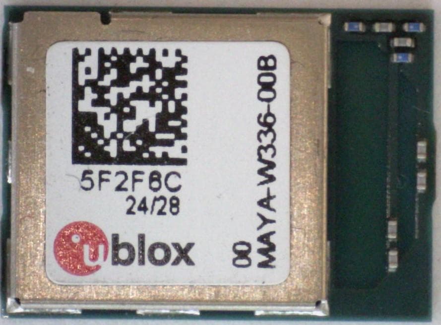
XPYMAYAW3A
Feb 01, 2026WLAN and Bluetooth module
Equipment Class
6XD - 15E 6 GHz Low Power Indoor Client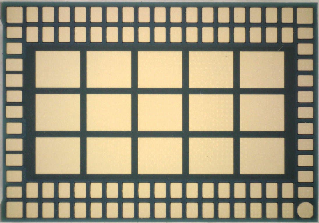
XPYJODYW6A
Jan 22, 2026WLAN and Bluetooth module
Equipment Class
NII - Unlicensed National Information Infrastructure TXXPYUBX22VA03
Jul 22, 2024NB CatM EGPRS data only module
Equipment Class
PCB - PCS Licensed Transmitter
XPYIRISW1
Jul 21, 2024Stand-alone Tri-radio wireless MCU module
Equipment Class
DTS - Digital Transmission System